BACKGROUND OF THE INVENTION
The present application claims priority from a
Japanese Patent Applications Nos. 2002-245324 filed on August
26, 2002 and 2003-175095 filed on June 19, 2003, the contents
of which are incorporated herein by reference.
Field of the Invention
The present invention relates to a data transferring
apparatus of liquid ejection data and a liquid ejection apparatus
having a data transferring apparatus of liquid ejection data
for transferring the liquid ejection data to a liquid ejection
head, wherein the liquid ej ection data is inputted into the liquid
ej ection apparatus which ejects liquid such as ink droplets from
the liquid ejection head onto a medium to be liquid-ejected.
Related Art
An inkjet type recording apparatus or printer
serving as a liquid ejection apparatus records image data by
ejecting ink from a recording head onto a recording sheet or
the like. The inkjet type printer ejects ink droplets of plural
colors from plural nozzle arrays of which is provided on a head
face of the recording head as developing image data, which has
been compressed to be capable of being developed in line, to
bitmap images in line and forming the developed bitmap images
on the recording side of the recording papers. It forms images
on the recording papers by ejecting ink droplets of plural colors
to form plural dots of ink. Further, the compressed data capable
of being developed in line is, for example, the compressed data
by the run length compression method which is generally widely
known or the compressed data by the compression method capable
of developing in consecutive order by bytes.
This inkjet type recording apparatus generally
includes a data transferring apparatus for receiving image data
compressed to be capable of being developed in line inputted
froman external apparatus suchas apersonal computer, developing
(extracting) the inputted compressed data in line, performing
data processes required for the developed bitmap images and then
transferring the data to a register of the recording head. The
generally conventional data transferring apparatus is
configured, for example, as shown in Fig. 36.
The data transferring apparatus 10 has a system bus
SB as a data transfer route . To the system bus SB a micro processor
(MPU) 11, a RAM 12 and a head controlling unit 13 are coupled
so as to transfer data, and a recording head 62 is coupled to
the head controlling unit 13. The compressed recording data
transferred from an information processing apparatus such as
a personal computer or a digital camera which is not shown in
drawings is stores in the RAM 12 via the system bus SB.
The compressed recording data stored in a compressed
data storing area of the RAM 12 is transferred to the micro
processor 11 via the system bus SB one byte each in order (a
route represented by symbol A), extracted by a program in
accordance with an extraction sequence one byte each in order,
then transferred to the RAM 12 via the system bus SB one byte
each in order once more (a route represented by the symbol B)
and then stored a desired bitmap image area of the RAM 12. When
the developed data has been completely stored in the bitmap image
area of the RAM 12, the developed data in the bitmap image area
of the RAM 12 is transferred to the register (not shown in drawings)
in the head controlling unit 13 via the system bus SB one byte
each (a route represented by the symbol C) and ink is ejected
from each of the nozzle arrays of the recording head 62 onto
the recording papers based on these bitmap images.
And, as an example of the prior art to speed up the
data transfer process, it is well-known that two independent
buses, a system bus and a local bus, are provided and two bus
controllers are provided between the system bus and the local
bus. In regard to the data transferring apparatus, parallel
processing is performed, that is, one bus controller accesses
a main memory which is coupled to the system bus while the other
bus controller accesses the local memory which is coupled to
the local bus so that the data transfer process speeds up as
shown, for example, in Japanese Patent No. 3251053.
To enhance the performance speed of liquid ejection
with regard to the data transferring apparatus 10 of the
conventional liquid ejection apparatus configured as shown in
Fig. 36, in other words, to further increase the recording speed
in regard to the inkjet type recording apparatus, there are some
obstacles as mentioned below.
First, since the compressed recording data is
developed (extracted) by a program one byte each, it is impossible
to process a great quantity of compressed data at high speed.
If the micro processor 11 which operates at high speed clock
and has a high process capacity is used speeding up can be achieved,
however, that causes such a problem as the cost of the data
transferring apparatus 10 gets extremely high if this expensive
micro processor 11 is mounted.
In addition, since both the data transfer to the
RAM 12 and the data transfer from the RAM 12 are performed through
the micro processor 11, while the micro processor 11 executes
other data processes or calculations such as the micro processor
11 fetches programs from the RAM 12, the data transfer might
get into a waiting state, and thus the data transfer delay occurs,
so that the data transfer at high speed cannot be achieved.
Further, since the same route is used for both the
access route from the micro processor 11 to the RAM 12 via the
system bus SB and the data transfer route from the RAM 12 to
the recording head 62, the system bus SB is occupied while the
micro processor 11 accesses the RAM 12, so that the data transfer
from the RAM 12 to the recording head 62 cannot be performed
during that time. For this reason, the data transfer delay to
the recording head 62 occurs, and thereby the data transfer rate
cannot speed up.
Moreover, in regard to the teaching of Japanese
Patent No. 3251053 described above, the compressed recording
data is still developed (extracted) by a program one byte each,
so that a great amount of compressed data cannot be developed
at high speed. Therefore, in regard to the liquid ejection
apparatus such as the recording apparatus which executes
recording by developing the compressed recording data
transferred from an information processing apparatus and then
transferring it to the recording head, the speed of ejecting
liquid cannot be enhanced because the process to develop the
compressed data is still slow though the data transfer process
can be performed at high speed.
The present invention has been achieved in view of
the situation above, and the solution is to realize the
development process of compressed data at high speed and the
data transfer to the liquid ejection head at high speed and to
considerably increase the liquid ejecting speed of the liquid
ejection apparatus compared with that of the prior art.
SUMMARY OF THE INVENTION
Therefore, it is an object of the present invention
to provide a data transferring apparatus of liquid ejection data
and a liquid ejection apparatus, which is capable of overcoming
the above drawbacks accompanying the conventional art. The
above and other obj ects can be achieved by combinations described
in the independent claims. The dependent claims define further
advantageous and exemplary combinations of the present
invention.
According to the first aspect of the present
invention, a data transferring apparatus of liquid ej ection data,
includes two independent buses which are a system bus and a local
bus, a main memory coupled to the system bus, capable of
transferring data, a local memory coupled to the local bus,
capable of transferring data and a decode unit comprising a decode
circuit coupled between the system bus and the local bus, capable
of transferring data mutually and developing liquid ejection
data compressed to be developed in line based on hardware.
First, the compressed liquid ejection data
developedby a conventional programbased on software is developed
by the decode circuit based on hardware. That is, by
independently performing only the development of the compressed
data by the decode circuit which is exclusively used for
developing compressed data rather than developing the compressed
data by a program of single thread which performs various data
processes in consecutive order besides the development process
of the compressed data, it is possible to perform the development
process of the compressed recording data at high speed.
In addition, by the configuration to have two
independent buses of the system bus and the local bus and the
local memory which is coupled to the local bus, it is possible
to secure the data transfer route of the liquid ejection data
from an independent memory to the liquid ejection head while
it is separated from an access route from a microprocessor to
a memory. Therefore, it is possible to perform the data transfer
from the local memory to a register of the liquid ejection head
through the local bus not synchronized with the system bus . Owing
to this, it is prevented that the data transfer from the memory
to the liquid ejection head gets interrupted by the access from
themicroprocessor to thememory so that the recordingperformance
speed gets low because the data transfer delay of liquid ejection
data occurs.
In this way, according to the data transferring
apparatus of liquid ejection data relating to the first aspect
of the present invention, by two independent buses, namely, the
system bus and the local bus and the decode unit incorporating
the decode circuit developing the compressed data, it is possible
to realize the development process of the compressed data at
high speed and the data transfer to the liquid ejection head
at high speed so that it is possible to increase the liquid ej ecting
speed of the liquid ejection apparatus considerably compared
with that of the prior art.
According to the second aspect of the present
invention, a data transferring apparatus of liquid ejection data,
includes two independent buses which are a system bus and a local
bus, a local memory coupled to the local bus, capable of
transferring data and a decode unit comprising a decode circuit
coupled between the system bus and the local bus, capable of
transferring data mutually and developing liquid ejection data
compressed to be developed in line based on hardware, a line
buffer for storing liquid ejection data developed by the decode
circuit per word unit and a DMA-transferring means for
DMA-transferringliquid ejection data compressed to be developed
in line from the main memory to the decode circuit,
DMA-transferring liquid ejection data developed in the line
buffer to the local memory per word unit and DMA-transferring
developed liquid ejection data stored in the local memory to
a register of an liquid ejection head sequentially.
First, the compressed liquid ejection data
developedby a conventional programbased on software is developed
by the decode circuit based on hardware. That is, by
independently performing only the development of the compressed
data by the decode circuit which is exclusively used for
developing compressed data rather than developing the compressed
data by a program of single thread which performs various data
processes in consecutive order besides the development process
of the compressed data, it is possible to perform the development
process of the compressed recording data at high speed.
In addition, the line buffer is provided to store
data after development per word unit, and the compressed data,
which used to be developed by the conventional program per one
byte, is developed per word unit (2 bytes), stored in the line
buffer and transferred to the local memory per word unit. That
is, the amount of compressed data, which is developed and
transferred at a time, gets twice that of the conventional way,
and thus it is possible to perform the development process of
compressed data at higher speed.
Further, by the configuration to have two
independent buses of the system bus and the local bus and the
local memory which is coupled to the local bus, it is possible
to secure the data transfer route of the liquid ejection data
from an independent memory to the liquid ejection head while
it is separated from an access route from a microprocessor to
a memory. Therefore, it is possible to perform the data transfer
from the local memory to a register of the liquid ejection head
through the local bus not synchronized with the systembus. Owing
to this, it is prevented that the data transfer from the memory
to the liquid ejection head gets interrupted by the access from
the microprocessor to the memory so that the recording performance
speed gets low because the data transfer delay of liquid ejection
data occurs.
Further, the high-speed data transfer can be
achieved by the DMA (Direct Memory Access) transfer. The DMA
transfer is such a well-known transfer method as once addresses
of a transfer source and a transfer destination or the number
of transfer are set in a register, then the data transfer can
be performed at high speed by hardware without the microprocessor.
In this way, according to the data transferring
apparatus of liquid ejection data relating to the second aspect
of the present invention, by two independent buses, namely, the
system bus and the local bus, the decode unit incorporating the
decode circuit and the DMA transferring means whereby the data
transfer can be performed at high speed by hardware without the
microprocessor, it is possible to realize the development process
of the compressed data at high speed and the data transfer to
the liquid ejection head at high speed so that it is possible
to increase the liquid ejecting speed of the liquid ejection
apparatus considerably compared with that of the prior art.
According to the third aspect of the present
invention, with respect to the second aspect described above,
registers of the main memory, the decode unit and the liquid
ejection head may be incorporated in an ASIC as a circuit block,
and registers of the decode unit and the liquid ejection head
may be coupled through an exclusive bus in the ASIC.
In this way, since the main memory, which stores
the compressed data, is configured to be the same block as the
decode unit in the ASIC, high DMA transfer can be achieved so
as to transfer data particularly with one clock. Therefore,
the compressed liquid ejection data can be transferred to the
decode unit at higher speed. In addition, since the registers
of the liquid ejection head are also incorporated in the same
ASIC as a circuit block, and coupled to the decode unit through
an exclusive bus in the ASIC, the data transfer of developed
liquid ejection data from the local memory to the liquid ejection
head can be performed at higher speed.
In this way, according to the data transferring
apparatus of liquid ejection data relating to the third aspect
of the present invention, the compressed liquid ejection data
can be transferred to the decode unit at higher speed, the data
transfer of developed liquid ejection data from the local memory
to the liquid ejection head can be performed at higher speed,
and thus it is possible to further increase the liquid ejecting
speed of the liquid ejection apparatus.
According to the fourth aspect of the present
invention, with respect to the second or third aspect described
above, the line buffer may comprise two sides of buffer areas
capable of storing developed data of predetermined words, liquid
ejection data developed by the decode circuit is sequentially
stored in one of the sides and liquid ejection data developed
by the decode circuit is sequentially stored in the other of
the sides when developed data of predetermined words has been
accumulated, while developed data of predetermined words is
DMA-transferred to the local memory for each predetermined words
when developed data of predetermined words has been accumulated.
In this way, the line buffer has two sides of buffer
areas which are capable of storing the developed data of
predetermined bytes, and stores the data which has been developed
by the decode circuit in one of those sides, and when predetermined
bytes have been accumulated, the developed data of one side is
transferred per word unit by the DMA transferring means, while
the data developed by the decoded circuit can be stored in the
other side, so that it is possible to perform development process
of compressed recording data and data transfer process in
parallel.
In this way, according to the data transferring
apparatus of liquid ejection data relating to the fourth aspect
of the present invention, development process of compressed
recording data and data transfer process can be perform in
parallel, and thus it is possible to further increase the liquid
ejecting speed of the liquid ejection apparatus.
According to the fifth aspect of the present
invention, in regard to any of the second to fourth aspects
described above, data transfers with respect to the local bus
from the decode circuit to the local memory and from the local
memory to a register of the liquid ejection head may be performed
in a burst transfer.
The burst transfer is such a data transfer method
which is a well-known method for speeding up the data transfer
as, when the continuous data is transferred, the data is
transferred while a bus is occupied until all data of a
predetermined data block is completely transferred by omitting
a part of a sequence such as an address designation so as to
increase the data transfer speed. And, since the data transfer
to the liquid ejection head performed via the system bus in the
conventional method is per formed via the local bus separated
from the system bus, the data transfers from the decode unit
to the local memory via the local bus and from the local memory
to the register of the liquid ejection head can be performed
in the burst transfer.
In this way, according to the data transferring
apparatus of liquid ejection data relating to the fifth aspect
of the present invention, the data transfers to the liquid
ejection head via the local bus can be performed in the burst
transfer, and thus it is possible to further increase the liquid
ejecting speed of the liquid ejection apparatus.
In addition, since the system bus and the local are
independent each other, and the data transfer to the register
of the liquid ejection head not synchronized with the system
bus can be perform by the decode circuit of the decode unit and
the line buffer, it is possible to maximize the effect of
increasing the liquid ejecting speed of the liquid ejection
apparatus.
According to the sixth aspect of the present
invention, in regard to any of the second to fifth aspects
described above, the compressed liquid ejection data may be run
length compressed data, and the decode circuit may be capable
of developing run length compressed data based on hardware.
Consequently, by the decode circuit whereby the run
length compressed data capable of being developed in line can
be developed based on hardware, the effect described in any of
the first to fifth aspects can be achieved.
According to the sixth aspect of the present
invention, in regard to any of the second to sixth aspects
described above, the decode unit may be comprise a means for
storing uncompressed liquid ejection data DMA-transferred from
the main memory without developing by the decode circuit based
on hardware.
Consequently, if the liquid ejection data stored
in the main memory is uncompressed data, a means stores it the
line buffer as it is without developing by the decode circuit
based on hardware, and thus it is possible to further increase
the liquid ejecting speed of the liquid ejection apparatus in
regard to the uncompressed liquid ejection data.
According to the eighth aspect of the present
invention, a liquid ejection apparatus comprises the data
transferring apparatus of liquid ejection data in regard to any
of the first to seven aspects described above.
Consequently, the effect described in any of the
first to seventh aspects can be achieved in regard to the liquid
ejection apparatus.
The summary of the invention does not necessarily
describe all necessary features of the present invention. The
present invention may also be a sub-combination of the features
described above. The above and other features and advantages
of the present invention will become more apparent from the
following description of the embodiments taken in conjunction
with the accompanying drawings.
BRIEF DESCRIPTION OF THE DRAWINGS
Fig. 1 is a plan view of an inkjet type recording
apparatus relating to the present invention.
Fig. 2 is a side view of an inkjet type recording
apparatus relating to the present invention.
Fig. 3 is a flowchart of the inkjet type recording
apparatus relating to the present invention.
Fig. 4 is a block diagram showing the configuration
of a data transferring apparatus relating to the present
invention.
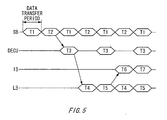
Fig. 5 is a timing chart showing the flow of recording
data.
Fig. 6 is a block diagram showing the configuration
of the DECU relating to the present invention.
Fig. 7 is a diagram showing such flow as compressed
recording data is developed.
Fig. 8 is a diagram showing such flow as compressed
recording data is developed.
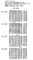
Figs. 9A to 9D are diagrams showing the recording
data after development.
Figs. 10A to 10D are diagrams showing the recording
data after development.
Fig. 11 is a diagram showing such flow as compressed
recording data is developed.
Fig. 12 is a diagram showing such flow as compressed
recording data is developed.
Fig. 13 is a diagram showing such flow as compressed
recording data is developed.
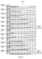
Fig. 14 is a diagram showing such flow as compressed
recording data is developed.
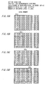
Figs. 15A to 15D are diagrams showing the recording
data after development.
Figs. 16A to 16D are diagrams showing the recording
data after development.
Fig. 17 is a diagram showing such flow as compressed
recording data is developed.
Fig. 18 is a diagram showing such flow as compressed
recording data is developed.
Fig. 19 is a diagram showing such flow as compressed
recording data is developed.
Fig. 20 is a diagram showing such flow as compressed
recording data is developed.
Figs. 21A to 21D are diagrams showing the recording
data after development.
Fig. 22 is a diagram showing such flow as compressed
recording data is developed.
Fig. 23 is a diagram showing such flow as compressed
recording data is developed.
Figs. 24A to 24 D are diagrams showing the recording
data after development.
Fig. 25 is a diagram showing such flow as compressed
recording data is developed.
Fig. 26 is a diagram showing such flow as compressed
recording data is developed.
Fig. 27 is a diagram showing such flow as compressed
recording data is developed.
Fig. 28 is a diagram showing such flow as compressed
recording data is developed.
Figs. 29A to 29D are diagrams showing the recording
data after development.
Figs. 30A to 30D are diagrams showing the recording
data after development.
Figs. 31A to 31D are diagrams showing the recording
data after development.
Figs. 32A to 32D are diagrams showing the recording
data after development.
Figs. 33A to 33D are diagrams showing the recording
data after development.
Figs. 34A to 34 D are diagrams showing the recording
data after development.
Fig. 35 is a diagram showing the state in which
uncompressed data is transferred.
Fig.36 is ablockdiagramshowingadata transferring
apparatus in regard to the prior art.
DETAILED DESCRIPTION OF THE INVENTION
The invention will now be described based on the
preferred embodiments, which do not intend to limit the scope
of the present invention, but exemplify the invention. All of
the features and the combinations thereof described in the
embodiment are not necessarily essential to the invention.
To begin with, a first embodiment of the inkjet type
recording apparatus or printer will be described as "liquid
ejection apparatus" relating to the present invention. Fig.
1 is a schematic plan view of an inkjet type recording apparatus
relating to the present invention, and Fig. 2 is a side view
thereof.
In the inkjet type apparatus 50, a carriage 61 is
provided to move along a main scanning direction X as a recording
means which performs recording on recording papers P, rotatably
supported by carriage guide shaft 51. On the carriage 61, a
recording head 62 is mounted as a "liquid ejection head" which
performs recording by ejecting ink onto the recording papers
P. Opposite to the recording head 62, a platen 52 is provided
to control a gap between the head surface of the recording head
62 and the recording papers P. A recording on the recording
papers P is performed by repeating an operation of carrying the
recording papers P between the carriage 61 and the platen 52
in a sub scanning direction Y a predetermined amount each and
an operation of ejecting ink droplets onto the recording papers
P from the recording head 62 while the recording head 62 moves
back and forth once in the main scanning direction X.
A paper feeding tray 57 is configured to be capable
of feeding the recording papers P such as normal papers or foot
papers, and a ASF (auto sheet feeder) is provided in it as a
paper feeding means to automatically feed the recording papers
P. The ASF is an automatic paper feeding mechanism which has
two paper feeding rollers 57b provided in the paper feeding tray
57 and a separating pad not shown in drawings. One of these
two paper feeding rollers 57b is arranged at the one side of
the paper feeding tray 57 while the other one of the paper feeding
rollers 57b is installed at a recording paper guide 57a, and
the recording paper guide 57a is provided at the paper feeding
tray 57 to be capable of sliding in the longitudinal direction
corresponding to the width of the recording papers P. And, by
the rotation drive force of the paper feeding roller 57b and
the frictional resistance of the separating pad, the plural
recording papers P stacked in the paper feeding tray 57 are
automatically and accurately fed not all but a piece each during
feeding.
As a recording paper carrying means for carrying
the recording papers P in the sub scanning direction Y, a driving
transfer roller 53 and driven transfer rollers 54 are provided.
The driving transfer roller 53 is rotatably controlled by the
rotation drive force such as a stepping motor, and by the rotation
of the driving transfer roller 53 the recording papers P are
carried in the sub scanning direction Y. The driven transfer
rollers 54 are provided as plural pieces, and each of them is
urged by the driving transfer roller 53 to rotate in contact
with the recording papers P as following the carriage of the
recording papers P when the recording papers P are carried by
the rotation of the driving transfer roller 53. On the surface
of the driving transfer roller 53, a film which has high frictional
resistance is provided. By the driven transfer rollers 54, the
recording papers P pressed onto the surface of the driving
transfer roller 53 are firmly in contact with the surface of
the driving transfer roller 53 so that they are carried in the
sub scanning direction Y by the rotation of the driving transfer
roller 53.
And, a sheet sensor 63 is provided between the paper
feeding roller 57b and the driving transfer roller 53 in the
well-known art. The sheet sensor 63 has a lever to which a
self-resetting characteristic into an upright position is
granted pivotally supported to be rotatable only in the recording
paper feeding direction as projecting toward the carriage route
of the recording papers P, and is configured as the end of the
lever is pushed toward the recording papers P and thus the lever
is rotated so that the recording papers P are detected. The
sheet sensor 63 detects the starting end position and the terminal
end position of the recording papers P fed by the paper feeding
roller 57b, and determines a recording area corresponding to
the detected positions to perform recording.
Meanwhile, a paper discharge driving roller 55 and
driven paper discharging rollers 56 are provided as a means for
discharging the recording papers P which have been recorded.
The paper discharge driving roller 55 is rotatably controlled
by the rotation drive force such as a stepping motor, and by
the rotation of the paper discharge driving roller 55 the
recording papers P are carried in the sub scanning direction
Y. The driven paper discharging rollers 56 have plural teeth
on their circumference, and becomes a toothed roller in which
the end of each tooth is sharp in an acute angle to be in contact
with the recording surface of a recording paper P at point. Each
of the plural driven paper discharging rollers 56 is urged by
the paper discharge driving roller 55 to rotate in contact with
the recording papers P as following the discharge of the recording
papers P when the recording papers P are carried by the rotation
of the paper discharge driving roller 55.
And, the rotation drivingmotor not shown in drawings
which rotatably drives the paper feeding roller 57b or the driving
transfer roller 53 and the paper discharge driving roller 55
and the carriage driving motor not shown in drawings which drives
the carriage 61 in the main scanning direction are controlled
by the recording controlling unit 100. In addition, the
recording head is also controlled by the recording controlling
unit 100 to ej ecting ink droplets onto the surface of the recording
papers P.
Fig. 3 is a schematic flowchart of the inkjet type
recording apparatus 50 relating to the present invention.
The inkjet type recording apparatus 50 has a
recording controlling unit 100 for controlling various recording
processes. The recording controlling unit 100 has two
independent buses, namely, a system bus SB and a local bus LB.
To the system bus SB a MPU (micro processor) 24, a ROM 21, a
RAM 22, a nonvolatile storage medium 23, I/O 25 and a decode
circuit 28 are coupled so as to be capable of transferring data.
In the MPU 24 various calculation processes are performed. In
the ROM 21, software/ program and data needed for calculation
processes of the MPU 24 are stored beforehand. The RAM 22 is
used as a temporarily storing area for the software/program or
a working area for the MPU 24 . In the nonvolatile storage medium
23 such as a flash memory some data resulting from the calculation
processes of the MPU 24 is stored, and it is designed to hold
the data even if the power of the inkjet type recording apparatus
50 is turned off.
Further, the recording controlling unit 100 is
configured to coupled to an information processing apparatus
200 such as a personal computer via an interface unit 27 which
has an interface function with external apparatuses, and to be
capable of processing input and output of various kinds of
information or data via the system bus SB with the information
processing apparatus 200. And, I/O 25 performs output control
to a various motors controlling unit 31 via an input and/or output
unit 26 based on the calculation process result of the MPU 24,
and allows input information to be inputted from various sensors
32. The various motors controlling unit 31 is a drive control
circuit which controls various motors of the inkj et type apparatus
50, and is controlled by the recording controlling unit 100.
Further, the various sensors 32 detect various kinds of condition
information of the inkjet type recording apparatus 50 and output
them to the I/O 25 via the input and/or output unit 26.
During performing recording, the information
processing apparatus 200 plays a host part to output recording
data (liquid ejection data) compressed by the information
processing apparatus 200, and the inkjet type apparatus 50
receives the compressed recording data from the interface unit
27 via the system bus SB. The decode circuit 28 develops the
compressed recording data and then stores the developed recording
data in a local memory 29 via the local bus LB. the developed
recording data stored in the local memory 29 is transferred again
from a register in a head controlling unit 33 to the recording
head 62 via the local bus LB. The head controlling unit 33
controls the recording head 62 to eject ink droplets of various
colors onto he recording papers P from the plural nozzle arrays
provided on the head side of the recording head 62.
In this way, by two independent buses, namely, the
system bus SB and the local bus LB and the decode circuit 28
developing the compressed data, it is possible to realize the
development process of the compressed data at high speed and
the data transfer to the recording head 62 at high speed so that
it is possible to increase the liquid ejecting speed of the inkj et
type recording apparatus 50 considerably compared with that of
the conventional art. In the end, by not developing the
compressed data by a program of single thread which performs
various data processes in consecutive order besides the
development process of the compressed data in regard to the MPU
24 in the conventional way but independently performing only
the development of the compressed data by the decode circuit
28 which is exclusively used for developing compressed data,
it is possible to perform the development process of the
compressed recording data at high speed.
In addition, by the configuration to have two
independent buses of the system bus SB and the local bus LB and
the local memory 29 which is coupled to the local bus LB, it
is possible to secure the data transfer route of recording data
(local bus LB) to the recording head 62 which is separated from
the system bus SB which is coupled to the MPU 24. Therefore,
it is possible to perform the data transfer from the local memory
29 to the register of the recording head 62 through the local
bus LB not synchronized with the system bus SB. Owing to this,
it is prevented that the data transfer to the recording head
62 gets interrupted by the access from the MPU 24 to the RAM
22 so that the recording performance speed gets low because the
data transfer delay of recording data occurs.
Further, in the present embodiment, a line buffer
281 is provided to store data after development per word unit
between the decode circuit 28 and the local bus LB. The recording
data developed in the decode circuit 28 is temporarily stored
once in line buffer 281. The developed recording data stored
in the line buffer 281 is transferred to the local memory 29
via the local bus LB two words each. In this way, the line buffer
281 may provided to store data after development per word unit
between the decode circuit 28 and the local bus LB. By providing
the line buffer 281 to store data after development per word
unit, developing the compressed data, which used to be developed
by the conventional program per one byte, per word unit (2 bytes ) ,
storing the data in the line buffer 281 and transferring the
data to the local memory 29 per word unit, the amount of compressed
data which is developed and transferred at a time gets twice
that of the conventional way, and thus it is possible to perform
the development process of compressed data at higher speed, which
is desirable.
Fig. 4 is a block diagram showing the configuration
of a data transferring apparatus 10 as a "data transferring
apparatus of liquid ejection data" relating to the present
invention. Fig. 5 is a timing chart schematically showing the
flow of recording data in a data transferring apparatus 10.
The recording controlling unit 100 has a ASIC
(Application Specific Integrated Circuit) 4, and the ASIC 4
incorporates the interface unit 27 described above, the head
controlling unit 33 described above, a receiving buffer unit
42 and a DECU 41 as a "decode unit" relating to the present invention.
The DECU 41 incorporates the decode circuit 28 described above,
the line buffer 281 and a "DMA transferring means" (It will be
described in detail. ) . The system bus SB and the local bus LB
are 16 bits buses, and thus it is possible to transfer data of
1 word (2 bytes) per a predetermined data transfer period.
Hereinafter, with reference to the timing chart shown in Fig.
5, the flow of recording data in regard to the data transferring
apparatus 10 will be described.
The compressed recording data is DMA-transferred
from the information processing apparatus 200 to the receiving
buffer unit 42 as a "mainmemory" via the interface unit 27 through
the system bus SB one word each (symbol T1). As described above,
the DMA transfer is such a transfer method as once addresses
of a transfer source and a transfer destination or the number
of transfer are set in a register then the data transfer can
be performed at high speed by hardware without the MPU 24 . Next,
data is DMA-transferred from the receiving buffer unit 42 to
the DECU 41 via the system bus SB (symbol T2). Continuously,
in the DECU 41, the compressed data of 1 word is developed by
the decode circuit 28 based on hardware, and the developed
recording data is stored in the line buffer 281 (symbol T3) .
The recording data developed and stored in the line
buffer 281 is DMA-transferred to a bitmap area in the local memory
29 via the local bus LB with non-synchronization to the data
transfer through the system SB when the recording data stored
in the line buffer 281 has reached a predetermined amount (symbol
T4 ) . Continuously, the recording data as a bitmap data stored
in the bitmap area of the local memory 29 is DMA-transferred
again to the DECU 41 via the local bus LB (symbol T5), then
DMA-transferred from the DECU 41 to the head controlling unit
33 via the an internal bus IB (symbol T6) , then stored in a register
in the head controlling unit 33 and then DMA-transferred to the
recording head 62 (symbol T7).
In this way, the data transfer from the receiving
buffer unit 42 (the main memory) to the decode circuit 28, the
data transfer from the decode circuit 28 to the local memory
29 and the data transfer from the local memory 29 to the recording
head 62 may be performed by the DMA transfer, and thus data transfer
at higher speed can be achieved, which is more preferable. In
addition, since the "main memory" which stores the compressed
data is configured to be the same block as the DECU 41 in the
ASIC 41 as the receiving buffer unit 42, high DMA transfer can
be achieved so as to transfer data particularly with one clock.
Moreover, a part of the RAM 22 may be used for the "main memory"
without providing the receiving buffer unit 42 to the ASIC 41.
Fig. 6 is a block diagram showing the configuration
of the DECU 41 as the "decode unit" relating to the present
invention.
A S-DMA controller 411 as the "DMA transferring
means" described above is a controller for DMA transfer through
the system bus SB. By the S-DMA controller 411, the compressed
recording data stored in the receiving buffer unit 42 is
DMA-transferred to the development processing controller 412
one word each. The development processing controller 412
incorporates the decode circuit 28 and the line buffer 281
described above. the compressed recording data DMA-transferred
one word each by the S-DMA controller 411 from the receiving
buffer unit 42 is developed by the decode circuit 28 one word
each based on hardware, and the developed recording data is
accumulated in the line buffer 281.
In the same way, a L-DMA controller 413 as the "DMA
transferring means" is a controller for DMA transfer through
the local bus LB. In addition, a local memory controller 414
retrieves from data the local memory 29 coupled to the local
bus LB and controls writing in it. The recording data developed
and DMA-transferred to the local memory 29 is stores in the
predetermined bitmap area of the local memory 29.
In the same way, a I-DMA controller 415 is a
controller for DMA transfer through the internal bus IB which
is an exclusive bus between the DECU 41 in the ASIC and the head
controlling unit 33. The developed recording data stored in
the bitmap area of the local memory 29 is DMA-transferred to
the head controlling unit 33 through the local bus LB and the
internal bus IB via the local memory controller 414 by the I-DMA
controller 415, then stored in a register in the had controlling
unit 33 and then DMA-transferred to the recording head 62.
In addition, the DMA transfer from the line buffer
281 to the local memory 29 is transfer in burst by the L-DMA
controller 413, and the DMA transfer from the local memory 29
to the recording head 62 is transfer in burst by the I-DMA
controller 415. As described above, the burst transfer is such
a data transfer method as, when the continuous data is transferred,
the data is transferred occupying a bus until all data of a
predetermined data block is completely transferred by omitting
a part of a sequence such as an address designation. The L-DMA
controller 413 transfers in burst the developed recording data
of predetermined bytes one word each, occupying the local bus
LB until the predetermined bytes have been DMA-transferred to
the local memory 29, when the developed recording data of the
predetermined bytes has been accumulated in the line buffer 281.
The I-DMA controller 415 transfers in burst the developed
recording data stored in the bitmap area of the local memory
29 one word per a data block of predetermined bytes, occupying
the local bus LB until all of one data block has been completely
DMA-transferred to the recording head 62.
In case the burst transfer from the line buffer 281
to the local memory 29 and the burst transfer from the local
memory 29 to the recording head 62 compete each other, the burst
transfer from the local memory 29 to the recording head 62 has
priority, and thus during the burst transfer from the local memory
29 to the recording head 62 the burst transfer from the line
buffer 281 to the local memory 29 is temporarily stopped, so
that the ink ejecting operation from the nozzle arrays of the
recording head 62 based on the recording data from the local
memory 29 to the recording head 62 is not be interrupted.
In this way, by transferring data while occupying
the local bus LB until all data of a predetermined data block
is completely sent in regard to the recording head 62, such a
problem as data transfer by the request of the MPU 24 through
the system bus SB cannot be performed does not occur, and thus
it is possible to perform data transfer of recording data to
the recording head 62 at high speed.
Fig. 7 and Fig. 8 are diagrams schematically showing
the state until compressed recording data is developed in the
decoded circuit 28 based on hardware and stored in the line buffer
281 in the DECU 41 . In addition, Fig. 9 is a diagram schematically
showing the state until the developed recording data is
transferred and stored from the line buffer 281 to the local
memory 29.
In this embodiment, the compressed recording data
has been compressed by a run length compression method. The
run length compression method is a well-known data compression
method and it will be briefly described below. The run length
compressed data is compressed data of byte boundary, and has
a set of count (1 byte) and data (1 byte or bytes). In other
words, the run length compressed data is configured to first
have the count and then necessarily have the data. If the value
of the count is more than 128 (a negative constant), that is,
more than 80H, that means repeatedly developing the next data
of 1 byte, and thus the data of 1 byte following the count is
repeatedly developed as many times as 257 from which the value
of the count subtracted. On the other hand, if the value of
the count is less than 127, that is, less than 7FH, that means
continuing data to be developed as it is without repeating after
the count, and thus the data following the count is developed
as it is without repetition as many times as the value of the
count to which one is added.
Next, the configuration of the line buffer 281 will
be described. The line buffer 281 has two sides of data storing
areas of 9 words which combine storing areas of 8 words (16 bytes)
and preliminary storing areas of 1 word (2 bytes), and each of
sides is A side and B side respectively. The recording data
developed by the decode circuit 28 1 word each is stored in one
of the A side and the B side of the line buffer 281 one word
each in turn, and the data is turned to be stored into the other
side when the developed data has been accumulated to be a
predetermined amount, in the present embodiment 16 bytes. In
addition, the accumulated and developed data of 16 bytes, as
described above, is stored in a predetermined bitmap area of
the local memory 29.
In this way, the line buffer 281 has two sides of
buffer areas which are capable of storing the recording data
after development of 16 bytes, and stores the recording data
which has been developed by the decode circuit 28 in one of those
sides. And, when 16 bytes have been accumulated, while the
recording data after development of one side is transferred per
word unit by a DMA transferring means, the recording data
developed by the decoded circuit 28 can be stored in the other
side, so that it is possible to perform development process of
compressed recording data and data transfer process in parallel.
Continuously, run length compressed data taken for
example, the flow of recording data will be described, wherein
the compressed data is developed by the decode circuit 28, stored
in the line buffer 281 and stored from the line buffer 281 to
the local memory 29.
In the receiving buffer unit (main memory) 42, the
run length compressed recording data of 24 words (48 bytes) which
begins from FEH is stored. The run length compressed recording
data is DMA-transferred to the decode circuit 28 via the system
bus SB one word each, namely, two bytes each, developed based
on hardware and stored in the line buffer 281. In the present
embodiment, the data starting address of the run length compressed
data is an even address, and the data starting address of the
bitmap data (image data) in the local memory 29 is an even address.
And, the number of bytes of the data block DMA-transferred from
the line buffer 281 to the local memory 29 (the number of bytes
of 1 line) are 16 bytes.
Further, in the main memory, the line buffer 281
in the DECU 41 shown in Fig. 7 and the local memory 29 shown
in Fig. 9, the left top is an even address, and addresses gets
to be upper addresses in order from the left to the right, which
will be the same with that of drawings below.
Hereinafter, one word each will be described in order .
First, the compressed recording data of initial 1 word (FEH,
01H) DMA-transferred from the receiving buffer unit 42 to the
decode circuit 28 in the DECU 41 (Transfer S1). The FEH is the
count, and the 01H is the data. Since the value of the count
of FEH is 254, that is, larger than 128 and 257-254=3 times,
the data of 01H is repeatedly developed and 1 byte each is stored
in order in the A side of the line buffer 281. Next, the run
length compressed data DMA-transferred to the decode circuit
28 is 03H and 02H (Transfer S2) . The 03H is the count, and the
02H is the data. Since the value of the count of 03H is 3, that
is, smaller than 127 and 3+1=4 bytes, the data following the
count gets developed without repletion. That is, the data of
02H, 78H, 55H and 44H following the count 03H is developed as
it is without repetition, and stored in order in the A side of
the line buffer 281 (Transfers S2 to S4). The FBH which is the
upper part (odd address part) of the DMA-transferred word data
in the Transfer S4 is the count, and the next data of 1 byte
is repeatedly developed 6 times (257-251=6).
Continuously, the compressed recording data
DMA-transferred to the decode circuit 28 is FFH and FEH (Transfer
S5). The lower address (even address) of FFH is the data, besides
the data of the previous count of FBH. Therefore, FFH is
repeatedly developed 6 times, and stored in order in the A side
of the line buffer 281. And, the upper address (odd address)
of FEH is the count, and the next data of 1 byte is repeatedly
developed 3 times (257-254=3). Continuously, the compressed
recording data DMA-transferred to the decode circuit 28 is 11H
and 06H (Transfer S6). The lower address (even address) of 11H
is the data, besides the data of the previous count of FEH.
Therefore, 11H is repeatedly developed 3 times, and stored in
the A side of the line buffer 281. And, the upper address (odd
address) of 06H is the count, and the next data (66H, 12H, 77H,
45H, 89H, 10H and 55H) of 7 bytes (6+1=7) is developed as it
is without repetition, and stored in order in the B side of the
line buffer 281 (Transfers S7 to S10).
In the meantime, when the developed recording data
has been accumulated to be the number of bytes of 1 line in the
A side of the line buffer 281, namely, 16 bytes (at the Transfer
S6), the 16 bytes are DMA-transmitted to the local memory 29
one word each as a data block of the 1 line. At that time, the
L-DMA controller 413 (Fig. 6) transfers data in burst, occupying
the local bus LB until all the recording data after 1 line
development is completely DMA-transferred to the local memory
29 (Transfer D1). The recording data of 1 line transferred to
the local memory 29 is stored 1 word each in order in the
predetermined bitmap area of the local memory 29 at the first
of the even address from the lower address (Fig. 9A).
Continuously, the compressed recording data
DMA-transferred to the decode circuit 28 is 10H and FAH (Transfer
S11). The lower address (even address ) of 10H is the data, besides
the data of the previous count of FBH. Therefore, 10H is
repeatedly developed 6 times, and stored in order in the B side
of the line buffer 281. And, the upper address (odd address)
of FAH is the count, and the next data of 1 byte is repeatedly
developed 7 times (257-250=7). Continuously, the compressed
recording data DMA-transferred to the decode circuit 28 is 20H
and 08H (Transfer S12). The lower address (even address) of
20H is the data, besides the data of the previous count of FAH.
Therefore, 20H is repeatedly developed 7 times, and stored in
the B side of the line buffer 281, and when the accumulated data
in the B side has reached 16 bytes the remaining data gets stored
in order in the A side. And, the upper address (odd address)
of 08H is the count, and the next data (12H, 13H, 14H, 15H, 16H,
17H, 18H, 19H and 20H) of 9 bytes (8+1=9) is developed as it
is without repetition, and stored in order in the A side of the
line buffer 281 (Transfers S13 to S17 in Fig. 8).
In the mean time, when the developed recording data
has been accumulated to be the number of bytes of 1 line in the
B side of the line buffer 281, namely, 16 bytes (at the Transfer
S12), the 16 bytes are DMA-transmitted to the local memory 29
one word each as a data block of the 1 line. At that time, the
L-DMA controller 413 (Fig. 6) transfers data in burst, occupying
the local bus LB until all the recording data after 1 line
development is completely DMA-transferred to the local memory
29 (Transfer D2). The recording data of 1 line transferred to
the local memory 29 is stored 1 word each in order in the
predetermined bitmap area of the local memory 29 at the first
of the even address from the lower address (Fig. 9B).
Continuously, the compressed recording data
DMA-transferred to the decode circuit 28 is 11H and 02H (Transfer
S18). The lower address (even address) of 11H is the data, besides
the data of the previous count of FDH. Therefore, 11H is
repeatedly developed 3 times (257-254=3), and stored in the A
side of the line buffer 281, and when the accumulated data in
the A side has reached 16 bytes the remaining data gets stored
in order in the B side. And, the upper address (odd address)
of 02H is the count, and the next data (98H, BOH and F2H) of
3 bytes (2+1=3) is developed as it is without repetition, and
stored in order in the B side of the line buffer 281 (Transfers
S19 to S20).
In the mean time, when the developed recording data
has been accumulated to be the number of bytes of 1 line in the
A side of the line buffer 281, namely, 16 bytes (at the Transfer
S18), the 16 bytes are DMA-transmitted to the local memory 29
one word each as a data block of the 1 line. At that time, the
L-DMA controller 413 (Fig. 6) transfers data in burst, occupying
the local bus LB until all the recording data after 1 line
development is completely DMA-transferred to the local memory
29 (Transfer D3). The recording data of 1 line transferred to
the local memory 29 is stored 1 word each in order in the
predetermined bitmap area of the local memory 29 at the first
of the even address from the lower address (Fig. 9C).
Continuously, the compressed recording data
DMA-transferred to the decode circuit 28 is ABH and 03H (Transfer
S21) . The lower address (even address) of ABH is the data, besides
the data of the previous count of FCH (the upper address of the
Transfer S20) . Therefore, ABH is repeatedly developed 5 times
(257-252=5) , and stored in order i n the B side of the line buffer
281. And, the upper address (odd address) of 03H is the count,
and the next data (FFH, FEH, FCH and FDH) of 4 bytes (3+1=4)
is developed as it is without repetition, and stored in order
in the B side of the line buffer 281 (Transfers S22 to S23).
Continuously, the compressed recording data
DMA-transferred to the decode circuit 28 is FEH and FFH (Transfer
S24). The lower address (even address ) of FEH is the data, besides
the data of the count of FEH. Therefore, FFH is repeatedly
developed 3 times (257-254=3) , and stored in order in the B side
of the line buffer 281. When the developed recording data has
been accumulated to be the number of bytes of 1 line in the B
side of the line buffer 281, namely, 16 bytes (at the Transfer
S24), the 16 bytes are DMA-transmitted to the local memory 29
one word each as a data block of the 1 line. At that time, the
L-DMA controller 413 (Fig. 6) transfers data in burst, occupying
the local bus LB until all the recording data after 1 line
development is completely DMA-transferred to the local memory
29 (Transfer D4).
The recording data of 1 line transferred to the local
memory 29 is stored 1 word each in order in the predetermined
bitmap area of the local memory 29 at the first of the even address
from the lower address (Fig. 9D). And, when the recording data
of the bitmap data for ejecting ink with one main scanning pass
has been stored in the local memory 29, data is DMA-transferred
from the local memory 29 to the recording head 62. At this time,
the I-DMA controller 415 (Fig. 6) transfers data in burst,
occupying the local bus LB until all the recording data of the
bitmap data for ejecting ink with one main scanning pass is
completely DMA-transferred to the head controlling unit 33.
In this way, it is possible to performthe development
process of the compressed recording data at high speed by
developing the compressed recording data, which used to be
developed by the conventional program based on software, in the
decode circuit 28 based on hardware. In addition, since the
compressed recording data, which used to be developed one byte
each by the conventional program, is developed per word unit
(two bytes) , it is possible to perform the development process
of the compressed recording data at high speed. And, by the
configuration to have two independent buses, namely, the system
bus SB and the local bus LB and the local memory 29 which is
coupled to the local bus LB, it is possible to perform the data
transfer to the from the local memory 29 to the recording head
62 through the local bus LB not synchronized with the system
bus SB. Owing to this, it is prevented that the data transfer
to the recording head 62 gets interrupted by the access from
the MPU 24 to the RAM 22 so that the recording performance speed
gets low because the data transfer delay of recording data occurs.
Accordingly, since it is possible to realize the
development process of the compressed data at high speed and
the data transfer to the recording head 62 at high speed, it
is possible to increase the liquid ejecting speed of the inkjet
type recording apparatus 50 considerably compared with that of
the prior art. By the way, the data transfer speed to the recording
head 62, which was 1 Mbytes/sec in the prior art, can be high
up to 8 to 10 Mbytes/sec by the data transferring apparatus 10
relating to the present invention. Further, if the data
processing capacity of the recording head 62 is low, no matter
how fast the data transfer is performed, only the recording
performance speed corresponding to the data processing capacity
of the recording head 62 is obtained, and thus it is surely
necessary to provide a recording head 62 which has enough process
speed.
Next, as a second embodiment of the inkjet type
recording apparatus 50 relating to the present invention, added
to the first embodiment described above, when the developed
recording data DMA-transferred from the DECU 41 to the local
memory 29 is stored in the predetermined bitmap area, the data
of 1 line is not stored in order from the lower address of the
bitmap area (stored in a horizontal direction) but is changed
and stored in a vertical direction to be well-arranged for the
recording head 62.
Fig. 10 is a diagram schematically showing the state
until the developed recording data is transferred and stored
from the line buffer 281 to the local memory 29, and shows the
state in which the data of 1 line is changed and stored in a
vertical direction.
In the bitmap area of the local memory 29 which is
the DMA transfer destination, the transfer destination address
is individually set to each word of the developed recording data
stored in the line buffer 281 by the development processing
controller 412 (Fig. 6) in the DECU 41 in order that the data
of 1 line is stored to be arranged in a vertical direction. And,
the L-DMA controller 413 (Fig. 6) in the DECU 41 sets this
individual transfer destination address as the transfer
destination address of the DMA transfer, and DMA-transfers the
developed recording data stored in the line buffer 281 to the
local memory 29 one word each (data rearranging means).
In this way, when the recording data of 1 word (16
bytes) is DMA-transferred from the line buffer 281 to the local
memory 29, it is possible to perform rearrangement of the
necessary recording data instantly by performing rearrangement
of the recording data developed in the DECU 41, comparing it
with performing rearrangement of data in a memory 1 byte each
in order by the conventional program, and thus it is possible
to perform rearrangement of recording data at high speed.
Further, as a third embodiment of the inkjet type
recording apparatus 50 relating to the present invention, added
to the first or second embodiment described above, in case the
data starting address of the run length compressed recording
data stored in the receiving buffer unit 42 is an odd address,
a invalid data mask processing means for nullifying the initial
data of 1 byte of word data including the initial data of the
run length compressed data DMA-transferred from the receiving
buffer unit 42 to the decode circuit 28.
Fig. 11 and Fig. 12 are diagrams schematically
showing the state until the compressed recording data is developed
in the decode circuit 28 based on hardware and stored in the
line buffer 281, in case the data starting address of the
compressed recording data is an odd address.
The initial byte data (FEH) of the run length
compressed recording data stored in the receiving buffer unit
42 (main memory) is stored in the upper address (odd address)
of the initial word data. That is, in the lower address (even
address) of the word data including this initial byte data, the
data irrelevant to the recording data (AAH) is stored. However,
if one word each is DMA-transferred from the receiving buffer
unit 42 to the decode circuit 28, the even address cannot help
but be initially transferred. Therefore, if the initial word
data of the run length compressed recording data is developed
as it is by the decode circuit 28 based on hardware, the development
is performed in the state where the data irrelevant to the
recording data is included, and thus it is impossible to surely
develop the compressed recording data.
Here, in the development processing controller 412
(Fig. 6), the decode circuit 28 develops the irrelevant data
of lower address (even address) of the word data including the
initial byte data by nullifying it with masking. Further, if
initial data of 1 word is developed by the decode circuit as
it is, AAH becomes the count, and FEH becomes the data, so that
FEH can be surely developed by nullifying AAH.
Next,the compressedrecording dataDMA-transferred
to the decode circuit 28 is 01H and 03H (Transfer S31). The
lower address (even address) of 01H is the data, besides the
data of the previous count of FEH. Therefore, 01H is repeatedly
developed 3 times (257-254=3), and stored in order in the A side
of the line buffer 281. And, the upper address (odd address)
of 03H is the count, and the next data (02H, 78H, 55H and 44H)
of 4 bytes (3+1=4) is developed as it is without repetition,
and stored in order in the A side of the line buffer 281 (Transfers
S32 to S33). Then, in the same order as that of the first
embodiment, the run length compressed recording data is developed
one word each and stored in order in the line buffer 281 (Transfers
S32 to S54), and when the developed recording data has been
accumulated to be 1 line bytes (16 bytes) the data is
DMA-transferred to the local memory 29 (Transfers D1 to D4).
Further, it is preferable to judges whether the data starting
address of the run length compressed recording data stored in
the receiving buffer unit 42 is an odd address or not by, for
example, a firmware program which is performed by the MPU 24.
In this way, although the data starting address of
the run length compressed recording data stored in the receiving
buffer unit 42 is an odd address, it is possible to accurately
develop data from the first of the run length compressed recording
data in the decode circuit 28 based on hardware.
Further, as a fourth embodiment of the inkjet type
recording apparatus 50 relating to the present invention, added
to the first to third embodiments described above, the number
of bites of 1 line is an odd number.
Fig. 13 and Fig. 14 are diagrams schematically
showing the state until the compressed recording data is developed
in the decode circuit 28 based on hardware and stored in the
line buffer 281, in case the quantity of 1 line is 15 bytes in
regard to the first or second embodiment described above. In
addition, Fig. 15 is a diagram schematically showing the state
until the developed recording data is transferred and stored
from the line buffer 281 to local memory 29 to be vertically
rearranged in line in regard to the fourth embodiment, and Fig.
16 is a diagram schematically showing the state until the
developed recording data is stored without being vertically
rearranged in line.
As described above, since the developed recording
data is DMA-transferred one word each from the line buffer 281
to the local memory 29, the storage of the developed recording
data in the bitmap area of the local memory 29 is performed 1
word each, and thus the recording data of odd bytes cannot be
DMA-transferred from the DECU 41 to the local memory 29. Here,
in the development processing controller 412 (Fig. 6), the number
of bytes of 1 line of the line buffer is set to be an odd number,
in the present embodiment, 15 bytes, and when the developed
recording data is accumulated to be 15 bytes in the A or B side
of the line buffer 281 the DMA transfer to the local memory 29
is performed. Therefore, the upper address part (odd address
part) of the word data including the recording data of 15 bytes
gets DMA-transferred in the state of 00H (data storage ending
position shifting means).
Transfers S61 to S64 will not be described because
they are the same as the Transfers S1 to S4 in the first embodiment
(Fig. 7). Continuously, the compressed recording data
DMA-transferred to the decode circuit 28 is FFH and FEH (Transfer
S65) . The lower address (even address) of FFH is the data, besides
the data of the count of FBH. Therefore, FFH is repeatedly
developed 6 times (257-251=6), and stored in order in the A side
of the line buffer 281. And, the upper address (odd address)
of FFH is the count, and the next data is repeatedly developed
2 times (257-255=2) and stored in order in the A side of the
line buffer 281.
Continuously, the compressed recording data
DMA-transferred to the decode circuit 28 is 11H and 06H (Transfer
S66) . Theloweraddress (even address) of 11H is the data, besides
the data of the previous count of FFH. Therefore, FFH is
repeatedly developed 2 times, and stored in order in the A side
of the line buffer 281. And, the upper address (odd address)
of 06H is the count, and the next data (66H, 12H, 77H, 45H, 89H,
10H and 55H) of 7 bytes (6+1=7) is developed as it is without
repetition, and stored in order in the B side of the line buffer
281 (Transfers S67 to S70).
In the mean time, when the developed recording data
has been accumulated to be the number of bytes of 1 line in the
A side of the line buffer 281, namely, 15 bytes (at the Transfer
S66) , the 15 bytes are DMA-transmitted to the local memory 29
one word each as a data block of the 1 line. At that time, the
L-DMA controller 413 (Fig. 6) transfers data in burst, occupying
the local bus LB until all the recording data after 1 line
development is completely DMA-transferred to the local memory
29 (Transfer D1). The recording data of 1 line transferred to
the local memory 29 is vertically rearranged in line by the data
rearranging means described above and stored 1 word each in order
in the predetermined bitmap area of the local memory 29 at the
first of the even address from the lower address (Fig. 15A).
In addition, if the data is not vertically rearranged in line,
then it is stored in order as it is (Fig. 16A). Then, in the
same way, the run length compressed recording data is developed
by the decode circuit 28 based on hardware (Transfers S71 to
S84), and when the recording data developed in the line buffer
281 has been accumulated to be 1 line bytes (15 bytes) the data
is DMA-transferred to the local memory 29 (Transfers D2 to D4) .
Fig. 17 and Fig. 18 are diagrams schematically
showing the state until the compressed recording data is developed
in the decode circuit 28 based on hardware and stored in the
line buffer 281, in case the quantity of 1 line is 15 bytes in
regard to the third embodiment described above.
Transfers S91 to S94 will not be described because
they are the same as the Transfers S31 to S34 in the second
embodiment (Fig. 11). Continuously, the compressed recording
data DMA-transferred to the decode circuit 28 is FFH and 11H
(Transfer S95). The lower address (even address) of FFH is the
count, and the upper address (odd address) of 11H is the data.
Therefore, 11H is repeatedly developed 2 times (257-255=2), and
stored in order in the A side of the line buffer 281.
And, when the developed recording data has been
accumulated to be the number of bytes of 1 line in the A side
of the line buffer 281, namely, 15 bytes (at the Transfer S95) ,
the 15 bytes are DMA-transmitted to the local memory 29 one word
each as a data block of the 1 line. At that time, the L-DMA
controller 413 (Fig. 6) transfers data in burst, occupying the
local bus LB until all the recording data after 1 line development
is completely DMA-transferred to the local memory 29 (Transfer
D1). The recording data of 1 line transferred to the local memory
29 is vertically rearranged in line by the data rearranging means
described above and stored 1 word each in order in the
predetermined bitmap area of the local memory 29 at the first
oftheevenaddressfromtheloweraddress (Fig. 15A). Inaddition,
if the data is not vertically rearranged in line, then it is
stored in order as it is (Fig. 16A). Then, in the same way,
the run length compressed recording data is developed by the
decode circuit 28 based on hardware (Transfers S71 to S84), and
when the recording data developed in the line buffer 281 has
been accumulated to be 1 line bytes (15 bytes) the data is
DMA-transferred to the local memory 29 (Transfers D2 to D4).
In this way, since the recording data is
DMA-transferred to the local memory 29 when the recording data
developed in the line buffer 281 has been accumulated to be odd
bytes, the transfer is performed while the upper address of the
last word data is 00H, and thus the developed recording data
can be stored in the bitmap area of the local memory 29 in order
that the last 1 byte of 1 line is 00H and the recording data
of 1 line is odd bytes as the data starting address is an even
address as shown in Fig. 15D and Fig. 16D.
Further, as a fifth embodiment of the inkjet type
recording apparatus 50 relating to the present invention, added
to the second to fourth embodiments described above, the recording
data is stored in the bitmap area of the local memory 29 in order
that the recording data of 1 line is odd bytes as the data starting
address is an even address.
In the nozzle arrays arranged in numbers and provided
on the recording head 62, the colors of ink which is ejected
are determined for each of the nozzle arrays. In the mean time,
the recording data stored in the bitmap area of the local memory
29 becomes the data for each of the colors of ink corresponding
to each of the nozzle arrays of each line. And, in regard to
a means for correcting the lag of the ink ejecting timing caused
by the nozzle arrays, there is a case that it is necessary to
store the recording data of 1 line in the bitmap area of the
local memory 29 letting the initial address be an odd address.
However, as described above, by DMA-transmitting
one word each from the receiving buffer unit 42 to the decode
circuit 28, the recording data developed in the bitmap area of
the local memory 29 is stored while an even address is always
positioned at the first, and thus in this state the recording
data cannot be stored while an odd address is positioned at the
first. Here, in the development controller 412 (Fig. 6), when
the recording data developed in the decode circuit 28 is stored
in the line buffer 281, it is stored from the 1-th byte of the
line buffer 281 in the state where the 0-th byte is vacant (data
storage starting position shifting method). That is, when the
developed recording data is stored in the line buffer 281 after
the compressed recording data is developed in the decode circuit
28, it is stored from the 1-th byte of the line buffer 281 in
the state where the 0-th byte is vacant, and the developed
recording data stored in the line buffer 281 is DMA-transferred
to the bitmap area of the local memory 29 from the 0-th byte
of the line buffer 281.
Fig. 19 and Fig. 20 are diagrams schematically
showing the state until the compressed recording data is developed
in the decode circuit 28 based on hardware and stored in the
line buffer 281, in case the recording data is developed from
the 1-th byte of the line buffer 281 in the state where the 0-th
byte is vacant in regard to the second embodiment described above.
In addition, Fig . 21 is a diagram schematically showing the state
until the developed recording data of 1 line, 16 bytes, is
transferred from the line buffer 281 to the local memory 29,
and vertically rearranged in line and stored while an odd address
comes first.
As described above, the line buffer 281 has a reserve
storage area of 1 word (2 bytes) which is added to the storage
area of 8 words (16 bytes) for both of the A and B sides. The
recording data developed 1 word each in the decode circuit 28
is stored from the 1-th byte in the state where the 0-th byte
of the A side of the line buffer is vacant. And, the 16-th byte
of the recording data, which cannot help but be forced out from
the storage area as the 0-th byte is made vacant, gets stored
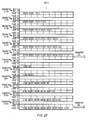
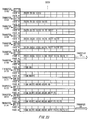
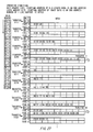
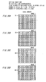
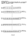
in the reserve storage area.
When the developed recording data has been
accumulated to be 16 bytes in the A side of the line buffer 281,
the 18 bytes (9 words) of the recording data in total, that is,
the 16 bytes in the storage area and the data in the reserve
storage area are DMA-transmitted to the local memory 29 one word
each as a data block of the 1 line. At that time, the L-DMA
controller 413 (Fig. 6) transfers data in burst, occupying the
local bus LB until all the recording data after 1 line development
is completely DMA-transferred to the local memory 29 (Transfer
D1) . The recording data of 1 line transferred to the local memory
29 is vertically rearranged in line by the data rearranging means
described above and stored 1 word each in order in the
predetermined bitmap area of the local memory 29 at the first
of the even address from the lower address (Fig. 21A). Therefore,
since data to which the vacant data of 1 byte at the first is
DMA-transferred to the local memory 29 and stored at the even
address of the bitmap area, the initial data of the recording
data of 1 line gets to be stored from the even address.
Then, in the same way, the run length compressed
recording data is developed by the decode circuit 28 based on
hardware, and when the recording data developed in the line buffer
281 has been accumulated to be 1 line bytes, 16 bytes, the data
is DMA-transferred to the local memory 29 (Transfers D2 to D4).
Further, transfers S121 to S144 will not be described because
they are the same as the Transfers S1 to S24 shown in Fig. 7.
In this way, since the recording data developed one
word each in the decode circuit 28 is stored from the 1-th byte
of the line buffer 281 in the state where the 0-th byte of the
A side of the line buffer 281 is vacant, and it is DMA-transferred
to the local memory 29 when the developed recording data of 16
bytes has been stored, the transfer is performed while the lower
address of the first word data is 00H, and thus the developed
recording data can be stored in the bitmap area of the local
memory 29 in order that the first 1 byte of 1 line is 00H and
the recording data of 1 line is odd bytes as the data starting
address is an even address as shown in Fig. 21D.
Fig. 22 and Fig. 23 are diagrams schematically
showing the state until the compressed recording data is developed
in the decode circuit 28 based on hardware and stored in the
line buffer 281, in case the recording data is developed from
the 1-th byte of the line buffer 281 in the state where the 0-th
byte is vacant in regard to the fourth embodiment described above.
In addition, Fig. 24 is a diagram schematically showing the state
until the developed recording data of 1 line, 15 bytes, is
transferred from the line buffer 281 to the local memory 29,
and vertically rearranged in line and stored while an odd address
comes first.
In this way, the number of 1 line bytes can be 15
bytes, that is, odd bytes. Therefore, as shown in Fig. 24D,
the storage in the bitmap area of the local memory 29 can be
performed in order that the first 1 byte of 1 line is 00H and
the data starting address of the recording data of 1 line, 15
bytes, is an even address.
In addition, Fig. 25 and Fig. 26 are diagrams
schematically showing the state until the compressed recording
data is developed in the decode circuit 28 based on hardware
and stored in the line buffer 281, in case the recording data
is developed from the 1-th byte of the line buffer 281 in the
state where the 0-th byte is vacant in regard to the third
embodiment described above and the recording data of 1 line is
16 bytes. In the same way, Fig. 27 and Fig. 28 shows ones in
case the recording data is developed from the 1-th byte of the
line buffer 281 in the state where the 0-th byte is vacant in
regard to the third embodiment described above and the recording
data of 1 line is 15 bytes.
In this way, after the compressed recording data
stored in the receiving buffer unit 42 while an odd address comes
first is developed in the decode circuit 28, the recording data
of 1 line, 15 or 16 bytes, can be stored in the bitmap area of
the local memory 29 while an odd address comes first.
Further, as a sixth embodiment of the inkjet type
recording apparatus 50 relating to the present invention, added
to any of the first to fifth embodiments described above, the
developed recording data is stored in two different bitmap areas
of the local memory 29. Fig. 29isadiagramschematicallyshowing
the state until the developed recording data of 1 line, 16 bytes,
is transferred from the line buffer 281 to the local memory 29,
and vertically rearranged in line and stored in the two different
bitmap areas while an even address comes first.
If a dot interval of the sub scanning direction Y
in regard to the developed bitmap data is smaller than an interval
of the nozzle arrays adjacent to the sub scanning direction Y,
the ink dots adjacent to the sub scanning direction Y cannot
be formed simultaneously by one main scan, and thus it is formed
during a different main scanning operation. However, since the
bitmap data developed in the decode circuit 28 has a data
configuration by which the ink ej ection data formed to be adj acent
to the sub scanning direction Y is continuously arranged,
recording cannot be performed while the developed bitmap data
is transferred to the recording head 62 as it is. For this reason,
it is necessary to divide the developed bitmap data in order
that the ink dot data adjacent to the sub scanning direction
Y can be transferred to the recording head 62 during a different
main scanning operation while it is stored in a different bitmap
area.
In this regard, two different bitmap areas are
provided in the local memory beforehand. In this embodiment,
they are represented by image 1 and image 2 respectively. In
regard to the bitmap area of the local memory 29 which is the
DMA transfer destination, the transfer destination addresses
are individually set for each one word of the developed recording
data stored in the line buffer 281 in the development processing
controller 41 (Fig. 6) in order that the data of 1 line is stored
in the image 1 and the image 2 in turn. And, the L-DMA controller
413 (Fig. 6) in the DECU 41 sets the individual transfer
destination address to be the transfer destination address of
DMA transfer, and DMA-transfers the developed recording data
stored in the line buffer 281 to local memory 29 one word each
(data dividing means).
First, when the developed recording data has been
accumulated in the A side of the line buffer 281 to be 1 line
of 16 bytes, the recording data of 1 line is DMA-transferred
to the local memory 29 (Transfer D1), and stored in the image
1 (Fig. 29A. Continuously, when the developed recording data
has been accumulated in the B side of the line buffer 281 to
be 1 line of 16 bytes, the recording data of 1 line is
DMA-transferred to the local memory 29 (Transfer D2), and stored
in the image 2 (Fig. 29B. Continuously, when the developed
recording data has been accumulated in the A side of the line
buffer 281 to be 1 line of 16 bytes, the recording data of 1
line is DMA-transferred to the local memory 29 (Transfer D3) ,
and stored in the image 1 (Fig. 29C). Continuously, when the
developed recording data has been accumulated in the B side of
the line buffer 281 to be 1 line of 16 bytes, the recording data
of 1 line is DMA-transferred to the local memory 29 (Transfer
D4), and stored in the image 2 (Fig. 29D).
In this way, the developed recording data stored
in the line buffer 281 after the compressed recording data is
developed is DMA-transferred to the different bitmap areas of
the local memory 29 one line each in order that each of the ink
dots adjacent to the sub scanning direction Y is formed during
the different main scanning operations respectively. Owing to
this, the development process of the compressed recording data
(in the decode circuit 28) and the division of the developed
recording data (in the development processing controller 412)
can be performed at high speed by a hardware process. In addition,
Fig. 30 is a diagram schematically showing the state until the
developed recording data of 1 line, 16 bytes, is transferred
from the line buffer 281 to the local memory 29, and stored in
the two different bitmap areas, while an even address comes first,
as it is without being vertically rearranged in line.
In addition, Fig. 31 is a diagram schematically
showing the state until the developed recording data of 1 line,
16 bytes, is transferred from the line buffer 281 to the local
memory 29, and vertically rearranged in line and stored in the
two different bitmap areas, while an even address comes first.
Fig. 32 is a diagram schematically showing the state until the
developed recording data of 1 line, 15 bytes, is transferred
from the line buffer 281 to the local memory 29, and stored in
the two different bitmap areas, while an even address comes first,
as it is without being vertically rearranged in line.
In this way, the developed recording data of odd
bytes, as the number of bytes of 1 line is an odd number, is
DMA-transferred to the local memory 29 when it has been stored
in the line buffer 281, and thus the recording data of 1 line
is transformed while the upper address of the last word data
is 00H. Therefore, the developed recording data stored in the
bitmap area of the local memory 29 is stored in the two different
bitmap areas, the images 1 and 2, for each line in order that
the last 1 byte of 1 line is 00H and the recording data of 1
line is odd bytes as the data starting address is an odd address.
In addition, Fig. 33 is a diagram schematically
showing the state until the developed recording data of 1 line,
16 bytes, is transferred from the line buffer 281 to the local
memory 29, and vertically rearranged in line and stored in the
two different bitmap areas, while an odd address comes first.
Fig. 34 is a diagram schematically showing the state until the
developed recording data of 1 line, 15 bytes, is transferred
from the line buffer 281 to the local memory 29, and vertically
rearranged in line and stored in the two different bitmap areas,
while an odd address comes first.
In this way, since the recording data developed one
word each in the decode circuit 28 is stored from the 1-th byte
of the line buffer 281 in the state where the 0-th byte of the
A side of the line buffer 281 is vacant, and it is DMA-transferred
to the local memory 29 when the developed recording data of 16
bytes has been stored, the transfer is performed while the lower
address of the first word data is 00H, and thus the recording
data can be stored in each of the two different bitmap areas,
the image 1 and the image 2, of the local memory 29 in order
that the first 1 byte of 1 line is 00H and the data starting
address of the recording data of 1 line is an odd address.
Further, as a seventh embodiment of the inkjet type
recording apparatus 50 relating to the present invention, in
regard to any of the first to sixth embodiments described above,
if the recording data stored in the receiving buffer unit 42
is uncompressed data, it is stored in the bitmap area without
development process. Fig. 35 is a diagram schematically showing
the state where the uncompressed recording data is stored in
the line buffer 281 as it is, and DMA-transferred to the local
memory 29.
In this way, if the recording data transferred from
the information processing apparatus 200 to the receiving buffer
unit 42 is uncompressed data, it is stored in the line buffer
281 one word each as it is without development process by the
decode circuit 28. And then, like the case that the compressed
recording data is developed by the decode circuit 28, in regard
to the development processing controller (Fig. 6) , the recording
data can be, as shown by the second to sixth embodiments described
above, stored in the two different bitmap areas by being
rearranged or being stored in the local memory 29 as the initial
address is an odd address, while 1 line bytes are set to be 16
or 15 bytes.
Although the present invention has been described
by way of exemplary embodiments, it should be understood that
those skilled in the art might make many changes and substitutions
without departing from the spirit and the scope of the present
invention which is defined only by the appended claims.