EP1394581A1 - Optical waveguide manufacturing method - Google Patents
Optical waveguide manufacturing method Download PDFInfo
- Publication number
- EP1394581A1 EP1394581A1 EP03737498A EP03737498A EP1394581A1 EP 1394581 A1 EP1394581 A1 EP 1394581A1 EP 03737498 A EP03737498 A EP 03737498A EP 03737498 A EP03737498 A EP 03737498A EP 1394581 A1 EP1394581 A1 EP 1394581A1
- Authority
- EP
- European Patent Office
- Prior art keywords
- optical waveguide
- manufacturing
- etching
- core
- mask
- Prior art date
- Legal status (The legal status is an assumption and is not a legal conclusion. Google has not performed a legal analysis and makes no representation as to the accuracy of the status listed.)
- Withdrawn
Links
Images



Classifications
-
- G—PHYSICS
- G02—OPTICS
- G02B—OPTICAL ELEMENTS, SYSTEMS OR APPARATUS
- G02B6/00—Light guides; Structural details of arrangements comprising light guides and other optical elements, e.g. couplings
- G02B6/10—Light guides; Structural details of arrangements comprising light guides and other optical elements, e.g. couplings of the optical waveguide type
- G02B6/12—Light guides; Structural details of arrangements comprising light guides and other optical elements, e.g. couplings of the optical waveguide type of the integrated circuit kind
- G02B6/13—Integrated optical circuits characterised by the manufacturing method
- G02B6/136—Integrated optical circuits characterised by the manufacturing method by etching
-
- G—PHYSICS
- G02—OPTICS
- G02B—OPTICAL ELEMENTS, SYSTEMS OR APPARATUS
- G02B6/00—Light guides; Structural details of arrangements comprising light guides and other optical elements, e.g. couplings
- G02B6/10—Light guides; Structural details of arrangements comprising light guides and other optical elements, e.g. couplings of the optical waveguide type
- G02B6/12—Light guides; Structural details of arrangements comprising light guides and other optical elements, e.g. couplings of the optical waveguide type of the integrated circuit kind
- G02B2006/12166—Manufacturing methods
- G02B2006/12176—Etching
Definitions
- the present invention relates to a method for manufacturing optical waveguides having a low optical transmission loss.
- a problem encountered with the core layer formed with the above-mentioned multi-component glass is that the optical transmission loss of the optical waveguide tends to be large.
- dry etching is performed with a mask or a resist pattern provided over the core layer. During this process, large irregularities are formed on the periphery of the core pattern that has been formed and cause increase of the optical transmission loss of the optical waveguide.
- the method for manufacturing an optical waveguide of the present invention is one in which a patterned mask or a resist is placed on the surface of a core layer and then dry etching is performed, where the dry etching process includes etching and ashing.
- the dry etching process includes not only etching but also ashing, it is possible to reduce irregularities otherwise formed by etching. As a result, an optical waveguide with a small optical transmission loss can be provided.
- Fig. 1 is a perspective view to illustrate one of the manufacturing steps of the present invention.
- Substrate 1 is silicon or various types of glass, for example.
- various types of glass mean glass that contains at least one of alkaline elements, alkaline earth elements and rare earth elements.
- First clad 2 is formed with SiO 2 or various types of glass.
- the thermal expansion coefficients of substrate 1 and first clad 2 are different, thermal stress is sometimes caused. Accordingly, most preferable is that the thermal expansion coefficients of the two are equal, but they can be used when the thermal expansion coefficients are close.
- the first clad may be made by oxidizing silicon into SiO 2 .
- substrate 1 and first clad 2 may be made of the same material. Core pattern 3 is formed using SiO 2 or various types of glass and its refractive index is made slightly greater than that of first clad 2.
- FIG. 2 is a disassembled perspective view of an optical waveguide that has been formed.
- the cross section of core pattern 3 does not need to be rectangular; it can be trapezoidal.
- second clad 4 a material having a slightly smaller refractive index than that of core pattern 3 is used.
- the same material as used for first clad 2 may be used for second clad 4.
- core pattern 3 As the refractive index of core pattern 3 is greater than those of first clad 2 and second clad 4, light is confined inside the core pattern due to the difference of the refractive indices, and light transmission through core pattern 3 is enabled. When there are irregularities on the outer surface of core pattern 3, light is scattered by the irregularities and as a result optical transmission loss is caused. Consequently, it is preferable that the outer surface of core pattern 3 that guides light be smooth.
- substrate preparation step 301 substrate 1 is prepared.
- first clad formation step 302 first clad 2 is formed on substrate 1.
- substrate 1 may be made of the same material as that of first clad 2, in which case first clad formation step 302 can be omitted.
- core layer 5 is formed with various types of glass.
- Mask layer 6 is formed in the next mask layer formation step 304.
- Mask layer 6 is made of a metal such as silicon, titanium, tungsten, nickel or chromium, or a semiconductor or an alloy of these metals. A film is deposited by sputtering, vacuum deposition or other method.
- resist pattern 7 is formed by a photolithographic process by coating a resist.
- masking step 306 mask layer 6 is processed by dry etching using resist pattern 7 as the mask to obtain mask pattern 8.
- the thinner resist pattern 7 is, the higher the patterning accuracy becomes. Accordingly, when etching, it is preferable that the ratio of the etching rate of resist pattern 7 to the etching rate of mask layer 6 be smaller.
- core etching step 307 core pattern 3 is formed by dry etching core layer 5 via mask pattern 8. Core etching step 307 is described below in detail.
- etching gas gas that contains fluorocarbons such as CF 4 , CHF 3 or C 4 F 8 , a sulfur-based gas such as SF 6 , an inert gas such as Ar or Xe, and oxygen, hydrogen, or mixed gas of these gases can be considered.
- mask pattern 8 is a mask to be used for patterning of core layer 5 by etching. This mask pattern 8 is etched practically simultaneously when core layer 5 is etched. Generally speaking, the thinner mask pattern 8 is, the higher the patterning accuracy becomes.
- the ratio (hereinafter selective etching ratio) of the etching rate of core layer 5 to the etching rate of mask pattern 8 is as high as possible.
- mask pattern 8 is made of material that contains tungsten and silicon, it was possible to increase the selective etching ratio.
- mask layer 6 it is necessary to deposit a film of a material that contains tungsten and silicon. Film deposition of this multi-component material was performed by sputtering. Also, when etching was performed with etching gas that contains fluorocarbons such as CF 4 , CHF 3 and C 4 F 8 , a further higher selective etching ratio was obtained.
- core pattern 3 When forming core pattern 3 by dry etching, the following problems are encountered. That is, when etching glass that contains alkaline elements, alkaline earth elements or rare earth elements with a gas that contains fluorocarbons, sometimes irregularities attributable to those elements are caused on the outer surface of core pattern 3. To be more specific, when first glass that does not contain these elements and second glass that contains these elements are etched under the same conditions, flat etching can be performed on the first glass without any irregularities whereas, in the second glass, there occurs a case in which irregularities are generated disabling flat etching.
- Physical etching can be made dominant by mixing inert gas such as Ar or Xe in the etching gas and performing etching by using high density plasma generated by using inductively coupled plasma source, surface wave type plasma source, antenna type plasma source, magnetron type plasma source, helicon wave type plasma source, electron cyclotron resonance type plasma source, or magnetic neutral line type plasma source thereby enabling reduction of irregularities.
- inert gas such as Ar or Xe
- Fig. 7 shows the cross section as cut along the line X-X' in Fig. 4.
- adherent materials 9 behave like a mask during etching. Accordingly, as etching proceeds, irregularities 10 are formed on the surface of core layer 5 as illustrated in Fig. 8.
- Fig. 6 shows the cross section as cut along the line Y-Y' in Fig. 4. When there is no adherent 9, the core pattern will show a desired shape such as a rectangle in Fig. 5. However, adherent materials 9 will adhere on the outer surface of core pattern 3, too. As a result, as the etching proceeds, irregularities 10 are formed on the outer surface of core pattern 3 as illustrated in Fig. 6.
- the outer surface of core pattern 3 that guides light be smooth.
- irregularities 10 exist, light is scattered by irregularities 10 and causes optical transmission loss. In order to reduce optical transmission loss, it is necessary to remove or at least reduce irregularities 10. In order to reduce irregularities 10, it is necessary to remove adherent materials 9 that are produced during etching. These adherent materials 9 can be removed by ashing. When etching core layer 5 with CF 4 as the etching gas, irregularities 10 could be removed by ashing with an oxygen gas.
- etching conditions were set by using mixed gas of CF 4 and Ar, etching was performed for 10 minutes, adherent materials 9 accumulated on the surface during etching, and irregularities 10 have formed. In this case, etching was performed for 3 minutes under the same conditions followed by ashing for 3 minutes, and adherent materials 9 were removed.
- irregularities 10 can be reduced by including etching and ashing in core etching step 307.
- etching and ashing In order to increase the amount of etching while reducing irregularities 10, it is effective to alternately repeat etching and ashing such as first etching for 3 minutes, followed by ashing for 3 minutes, and then performing another round of etching for 3 minutes and ashing for 3 minutes.
- etching time of 3 minutes was given as an example it can be set at an arbitrary length, and the etching time and the ashing time can be different. Also, two or more combinations of different etching conditions and ashing conditions may be repeated for arbitrary lengths of time. For example, in the first step, etching is performed for 8 minutes under predetermined condition E01, and then etching is performed for 2 minutes under other condition E02, followed by ashing for 3 minutes under predetermined condition A01. In the subsequent second step, etching is performed for 5 minutes under condition E01 again, etching for 1 minute under condition E02, followed by ashing for 2 minutes under condition A01. Etching and ashing can be alternately repeated such as by subsequently performing the second cycle once more. By a process that effectively combines etching and ashing, irregularities 10 can be reduced and core pattern 3 of a desired configuration can be processed.
- Fig. 1 shows an example of a state in which core pattern 3 has been formed.
- second clad formation step 309 in Fig. 3 second clad 4 is formed to obtain an optical waveguide.
- two core patterns are shown as an example.
- Fig. 2 that illustrates a completed optical waveguide, only one core pattern is shown as an example.
- Core layer 5 is formed on first clad plate 2, and then mask pattern 8 is provided on the surface of core layer 5. Subsequently, core pattern 3 is formed by performing dry etching, and then second clad 4 is formed on first clad 2 in a manner such that it covers core pattern 3.
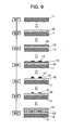
- first clad 12 is formed on substrate 11 in first clad formation step 902.
- core layer 15 is formed on first clad plate 2
- resist pattern 17 is provided on the surface of core layer 15.
- core etching step 905 core pattern 13 is formed by dry etching core layer 15.
- second clad 14 is formed on first clad 12 in second clad formation step 907 in a manner such that it covers core pattern 13 thus completing an optical waveguide.
- resist pattern 17 itself works as a mask for dry etching.
- an optical waveguide that has a core layer consisting of a glass material that contains alkaline elements, alkaline earth elements, or rare earth elements.
- an optical waveguide employing a core layer made of single crystal material that contains alkaline elements, alkaline earth elements, transition elements, or rare earth material is formed as shown in substrate preparation step 301 through mask removal step 309 of Fig. 3.
- the present invention features perfoming not only etching but also ashing in the dry etching step of the core layer in a method for manufacturing an optical waveguide in which a patterned mask or resist is provided on the surface of a core layer and then a core pattern is formed by performing dry etching. With this, irregularities that are formed when performing etching can be reduced.
- a glass material that contains at least one of the elements from alkaline elements, alkaline earth elements, or rare earth elements can be used.
- a single crystal material that contains at least two elements from alkaline elements, alkaline earth elements, transition elements, or rare earth elements may be used.
- the amount of etching can be increased while keeping irregularities small.
- the ratio of the etching rate of the core layer to the etching rate of mask or resist is called selective etching ratio.
- gas containing fluorocarbons such as CF 4 , CHF 3 or C 4 F 8 for etching, it is possible to increase the selective etching ratio to a relatively large value.
- the selective etching ratio can also be made relatively large.
- irregularities formed by etching can be further reduced by using mixed gas including inert gases such as Ar, Kr, and Xe. Moreover, by using oxygen-containing gas for ashing, the irregularities formed by etching can be further reduced.
- a mask layer can be formed with ease by sputtering. Also, by processing the mask by dry etching, a mask with an excellent configuration can be formed.
- the plasma source for use in a vacuum chamber at least one of inductively-coupled plasma source, surface wave plasma source, antenna type plasma source, magnetron type plasma source, helicon wave type plasma source, electron cyclotron resonance type plasma source, and magnetic neutral line type plasma source can be used.
- inductively-coupled plasma source surface wave plasma source, antenna type plasma source, magnetron type plasma source, helicon wave type plasma source, electron cyclotron resonance type plasma source, and magnetic neutral line type plasma source.
- formation of the first clad plate, second clad plate, or the core layer can be performed by using sputtering.
- the present invention enables reduction of irregularities formed by etching by including ashing in the dry etching process.
- the present invention is a method for manufacturing an optical waveguide by providing a mask or resist on the surface of a core layer followed by performing dry etching, in which the dry etching step includes etching and ashing processes.
- the dry etching step includes etching and ashing processes.
Landscapes
- Physics & Mathematics (AREA)
- Engineering & Computer Science (AREA)
- Microelectronics & Electronic Packaging (AREA)
- General Physics & Mathematics (AREA)
- Optics & Photonics (AREA)
- Optical Integrated Circuits (AREA)
Abstract
Description
Claims (21)
- A method for manufacturing an optical waveguide having a
core on a first clad, said method including the steps of:forming a core layer on said first clad;forming a mask for forming a mask pattern on the surface of said core layer;core etching for patterning said core layer by dry etching; whereinsaid core etching step includes an etching step and ashing step. - The method for manufacturing an optical waveguide of claim 1 wherein said core etching step includes one or more of said etching step or said ashing step and the final step is said ashing step.
- The method for manufacturing an optical waveguide of claim 1 wherein a second clad forming step is further included after said core etching step and said second clad covers said core.
- The method for manufacturing an optical waveguide of claim 3 wherein said second clad forming step is a step of forming said second clad by sputtering material selected from the group consisting of SiO2 and a glass material for covering said core.
- The method for manufacturing an optical waveguide of claim 1 wherein said dry etching is reactive ion etching.
- The method for manufacturing an optical waveguide of claim 1 wherein said etching step is performed by using a gas that contains fluorocarbons.
- The method for manufacturing an optical waveguide of claim 1 wherein said etching step is performed by using a mixed gas that contains fluorocarbons and an inert gas.
- The method for manufacturing an optical waveguide of claim 1 wherein said ashing step is performed by using a gas that contains oxygen.
- The method for manufacturing an optical waveguide of claim 1 wherein said dry etching is performed in a vacuum chamber by using generated plasma.
- The method for manufacturing an optical waveguide of claim 1 wherein said mask is any one or a combination of at least two selected from the group consisting of a resist film, metal film and semiconductor film.
- The method for manufacturing an optical waveguide of claim 1 wherein said mask is formed with material that contains tungsten and silicon.
- The method for manufacturing an optical waveguide of claim 1 wherein said mask forming step includes a step of forming a mask layer by sputtering.
- The method for manufacturing an optical waveguide of claim 1 wherein said mask forming step includes a step of patterning a formed mask layer by dry etching.
- The method for manufacturing an optical waveguide of claim 13 wherein said dry etching is reactive ion etching.
- The method for manufacturing an optical waveguide of claim 13 wherein said dry etching is performed in a vacuum chamber by using generated plasma.
- The method for manufacturing an optical waveguide of claim 13 wherein dry etching of said mask layer and dry etching of said core layer are performed in the same processing chamber.
- The method for manufacturing an optical waveguide of claim 1 wherein formation of said core layer is performed by sputtering.
- The method for manufacturing an optical waveguide of claim 1 wherein said optical waveguide is formed on a substrate and said first clad plate is formed on said substrate by sputtering.
- The method for manufacturing an optical waveguide of claim 1 wherein said core layer is glass material that contains at least one element selected from the group consisting of the alkaline elements, alkaline earth elements and rare earth elements.
- The method for manufacturing an optical waveguide of claim 1 wherein said core layer is single crystal material that contains at least one element selected from the group consisting of the alkaline elements, alkaline earth elements, transition elements and rare earth elements.
- The method for manufacturing an optical waveguide of claim 15 wherein said plasma is generated by using at least one plasma source selected from the group consisting of inductively-coupled plasma source, surface wave plasma source, antenna plasma source, magnetron plasma source, helicon wave plasma, electron cyclotron resonance plasma source and magnetic neutral line plasma source.
Applications Claiming Priority (3)
| Application Number | Priority Date | Filing Date | Title |
|---|---|---|---|
| JP2002029240 | 2002-02-06 | ||
| JP2002029240 | 2002-02-06 | ||
| PCT/JP2003/001174 WO2003067293A1 (en) | 2002-02-06 | 2003-02-05 | Optical waveguide manufacturing method |
Publications (2)
| Publication Number | Publication Date |
|---|---|
| EP1394581A1 true EP1394581A1 (en) | 2004-03-03 |
| EP1394581A4 EP1394581A4 (en) | 2006-12-13 |
Family
ID=27677882
Family Applications (1)
| Application Number | Title | Priority Date | Filing Date |
|---|---|---|---|
| EP03737498A Withdrawn EP1394581A4 (en) | 2002-02-06 | 2003-02-05 | METHOD FOR MANUFACTURING OPTICAL WAVEGUIDE |
Country Status (5)
| Country | Link |
|---|---|
| US (1) | US7095934B2 (en) |
| EP (1) | EP1394581A4 (en) |
| JP (1) | JPWO2003067293A1 (en) |
| CN (1) | CN1244828C (en) |
| WO (1) | WO2003067293A1 (en) |
Cited By (2)
| Publication number | Priority date | Publication date | Assignee | Title |
|---|---|---|---|---|
| TWI472818B (en) * | 2010-05-18 | 2015-02-11 | Unimicron Technology Corp | Manufacturing method of optoelectronic substrate |
| WO2018063708A1 (en) * | 2016-09-30 | 2018-04-05 | Intel Corporation | Fabrication process for ribbon bundled millimeter-waveguide |
Families Citing this family (1)
| Publication number | Priority date | Publication date | Assignee | Title |
|---|---|---|---|---|
| JP4852972B2 (en) * | 2005-10-26 | 2012-01-11 | パナソニック電工株式会社 | Optical component manufacturing method and light emitting device |
Family Cites Families (20)
| Publication number | Priority date | Publication date | Assignee | Title |
|---|---|---|---|---|
| JPS63116428A (en) | 1986-11-05 | 1988-05-20 | Hitachi Ltd | Dry etching method |
| DE3642073C1 (en) * | 1986-12-10 | 1988-02-04 | Heidenhain Gmbh Dr Johannes | Process for etching alkali glass layers by reactive plasma etching |
| JPH04161906A (en) * | 1990-10-25 | 1992-06-05 | Brother Ind Ltd | Light wave guide |
| JP3129855B2 (en) | 1992-10-12 | 2001-01-31 | 日立電線株式会社 | Method for manufacturing rare earth ion / alkali metal added glass substrate and method for manufacturing rare earth ion / alkali metal added glass waveguide |
| US5562838A (en) * | 1993-03-29 | 1996-10-08 | Martin Marietta Corporation | Optical light pipe and microwave waveguide interconnects in multichip modules formed using adaptive lithography |
| US5519802A (en) * | 1994-05-09 | 1996-05-21 | Deacon Research | Method for making devices having a pattern poled structure and pattern poled structure devices |
| JPH08262250A (en) | 1995-03-22 | 1996-10-11 | Toshiba Mach Co Ltd | Production of optical waveguide and device therefor |
| US5764842A (en) * | 1995-03-23 | 1998-06-09 | Hitachi, Ltd. | Semiconductor guided-wave optical device and method of fabricating thereof |
| US5563979A (en) * | 1995-08-31 | 1996-10-08 | Lucent Technologies Inc. | Erbium-doped planar optical device |
| JPH10261713A (en) | 1997-03-19 | 1998-09-29 | Sony Corp | Method for manufacturing semiconductor device |
| WO1998044166A1 (en) * | 1997-03-28 | 1998-10-08 | Citizen Watch Co., Ltd. | Method of manufacturing multistep substrate |
| KR100248055B1 (en) * | 1997-08-26 | 2000-03-15 | 윤종용 | Hybrid optical waveguide and manufacturing process |
| JP3333120B2 (en) | 1997-10-01 | 2002-10-07 | 住友大阪セメント株式会社 | Method for cleaning surface of plasma-etched composite oxide substrate |
| KR19990035454A (en) * | 1997-10-31 | 1999-05-15 | 윤종용 | How to fabricate planar optical waveguides in a single chamber |
| JP2000277493A (en) | 1999-03-26 | 2000-10-06 | Showa Denko Kk | Plasma etching method of semiconductor substrate and semicondcutor etching substrate |
| GB2348399A (en) * | 1999-03-31 | 2000-10-04 | Univ Glasgow | Reactive ion etching with control of etch gas flow rate, pressure and rf power |
| JP3575342B2 (en) | 1999-07-30 | 2004-10-13 | 日立電線株式会社 | Method for manufacturing silica glass optical waveguide |
| JP2001066450A (en) | 1999-08-31 | 2001-03-16 | Hitachi Cable Ltd | Manufacturing method of glass waveguide |
| JP2001257198A (en) | 2000-03-13 | 2001-09-21 | Matsushita Electric Ind Co Ltd | Plasma processing method |
| KR100561134B1 (en) * | 2001-03-08 | 2006-03-16 | 다이킨 고교 가부시키가이샤 | Optical Materials Including Curable Fluorine-Containing Polymers |
-
2003
- 2003-02-05 US US10/478,707 patent/US7095934B2/en not_active Expired - Fee Related
- 2003-02-05 EP EP03737498A patent/EP1394581A4/en not_active Withdrawn
- 2003-02-05 JP JP2003566588A patent/JPWO2003067293A1/en not_active Withdrawn
- 2003-02-05 CN CN03800527.1A patent/CN1244828C/en not_active Expired - Fee Related
- 2003-02-05 WO PCT/JP2003/001174 patent/WO2003067293A1/en not_active Ceased
Cited By (3)
| Publication number | Priority date | Publication date | Assignee | Title |
|---|---|---|---|---|
| TWI472818B (en) * | 2010-05-18 | 2015-02-11 | Unimicron Technology Corp | Manufacturing method of optoelectronic substrate |
| WO2018063708A1 (en) * | 2016-09-30 | 2018-04-05 | Intel Corporation | Fabrication process for ribbon bundled millimeter-waveguide |
| US10263312B2 (en) | 2016-09-30 | 2019-04-16 | Intel Corporation | Plurality of dielectric waveguides including dielectric waveguide cores for connecting first and second server boards |
Also Published As
| Publication number | Publication date |
|---|---|
| EP1394581A4 (en) | 2006-12-13 |
| US20040151458A1 (en) | 2004-08-05 |
| CN1244828C (en) | 2006-03-08 |
| JPWO2003067293A1 (en) | 2005-06-02 |
| WO2003067293A1 (en) | 2003-08-14 |
| CN1522377A (en) | 2004-08-18 |
| US7095934B2 (en) | 2006-08-22 |
Similar Documents
| Publication | Publication Date | Title |
|---|---|---|
| US4722878A (en) | Photomask material | |
| JP2001272505A (en) | Surface treatment method | |
| EP0190867B1 (en) | Process for manufacturing a photomask | |
| CN1122187C (en) | Method for making planar light guides in one chamber | |
| US4931077A (en) | Method of manufacturing a planar optical component | |
| JP2001291661A (en) | Reflective mask manufacturing method | |
| EP1258753A2 (en) | Silica-based optical wave guide circuit and fabrication method thereof | |
| US7095934B2 (en) | Optical waveguide manufacturing method | |
| JPH04246649A (en) | Photomask blank, production thereof, photomask and production thereof | |
| JP2002289592A (en) | Method for manufacturing semiconductor device | |
| EP0599394A1 (en) | Method of manufacturing sharp waveguide branches in integrated optical components | |
| JP3041802B2 (en) | Photomask blank and photomask | |
| JPH1020471A (en) | Manufacturing method of exposure mask | |
| AU744883B2 (en) | Method of forming a silicon layer on a surface | |
| JP2003035833A (en) | Silica-based optical waveguide circuit and method of manufacturing the same | |
| KR100472115B1 (en) | Blank-mask and its method for manufacturing | |
| JP2738121B2 (en) | Method for manufacturing silica-based optical waveguide | |
| KR20170047543A (en) | Method of manufacturing of LiNbO3 substrate for optical modulator | |
| JP3144666B2 (en) | Method for manufacturing silica-based glass optical waveguide | |
| JP4001416B2 (en) | Method for manufacturing buried planar lightwave circuit element | |
| US6180321B1 (en) | Method for patterning a thin film layer | |
| JP2004287173A (en) | Manufacturing method of optical waveguide | |
| JP2005037464A (en) | Optical waveguide and manufacturing method thereof | |
| JPH11211927A (en) | Optical waveguide manufacturing method | |
| JP2024118107A (en) | Metal oxide mask, its remover, and silicon nitride film patterning method |
Legal Events
| Date | Code | Title | Description |
|---|---|---|---|
| PUAI | Public reference made under article 153(3) epc to a published international application that has entered the european phase |
Free format text: ORIGINAL CODE: 0009012 |
|
| 17P | Request for examination filed |
Effective date: 20031223 |
|
| AK | Designated contracting states |
Kind code of ref document: A1 Designated state(s): AT BE BG CH CY CZ DE DK EE ES FI FR GB GR HU IE IT LI LU MC NL |
|
| AX | Request for extension of the european patent |
Extension state: AL LT LV MK RO |
|
| RBV | Designated contracting states (corrected) |
Designated state(s): AT BE BG CH CY CZ DE DK EE ES FI FR GB GR HU IE IT LI LU MC NL PT SE SI SK TR |
|
| A4 | Supplementary search report drawn up and despatched |
Effective date: 20061114 |
|
| 17Q | First examination report despatched |
Effective date: 20070222 |
|
| GRAP | Despatch of communication of intention to grant a patent |
Free format text: ORIGINAL CODE: EPIDOSNIGR1 |
|
| STAA | Information on the status of an ep patent application or granted ep patent |
Free format text: STATUS: THE APPLICATION IS DEEMED TO BE WITHDRAWN |
|
| 18D | Application deemed to be withdrawn |
Effective date: 20080404 |