EP1393176B1 - Method and apparatus for fault tolerant and flexible test signature generator - Google Patents
Method and apparatus for fault tolerant and flexible test signature generator Download PDFInfo
- Publication number
- EP1393176B1 EP1393176B1 EP02731860A EP02731860A EP1393176B1 EP 1393176 B1 EP1393176 B1 EP 1393176B1 EP 02731860 A EP02731860 A EP 02731860A EP 02731860 A EP02731860 A EP 02731860A EP 1393176 B1 EP1393176 B1 EP 1393176B1
- Authority
- EP
- European Patent Office
- Prior art keywords
- scan chains
- misr
- generator
- signal
- scan
- Prior art date
- Legal status (The legal status is an assumption and is not a legal conclusion. Google has not performed a legal analysis and makes no representation as to the accuracy of the status listed.)
- Expired - Lifetime
Links
- 238000012360 testing method Methods 0.000 title claims description 39
- 238000000034 method Methods 0.000 title description 7
- 230000004913 activation Effects 0.000 claims 2
- 238000001514 detection method Methods 0.000 claims 1
- 238000013461 design Methods 0.000 description 7
- 238000010586 diagram Methods 0.000 description 7
- 230000006870 function Effects 0.000 description 5
- 238000013481 data capture Methods 0.000 description 4
- 239000013598 vector Substances 0.000 description 4
- 238000004088 simulation Methods 0.000 description 3
- 230000007547 defect Effects 0.000 description 2
- 230000000694 effects Effects 0.000 description 2
- 238000004519 manufacturing process Methods 0.000 description 2
- 238000003775 Density Functional Theory Methods 0.000 description 1
- XUIMIQQOPSSXEZ-UHFFFAOYSA-N Silicon Chemical compound [Si] XUIMIQQOPSSXEZ-UHFFFAOYSA-N 0.000 description 1
- 230000002411 adverse Effects 0.000 description 1
- 230000006835 compression Effects 0.000 description 1
- 238000007906 compression Methods 0.000 description 1
- 230000003247 decreasing effect Effects 0.000 description 1
- 230000002950 deficient Effects 0.000 description 1
- 230000010354 integration Effects 0.000 description 1
- 238000005204 segregation Methods 0.000 description 1
- 239000004065 semiconductor Substances 0.000 description 1
- 229910052710 silicon Inorganic materials 0.000 description 1
- 239000010703 silicon Substances 0.000 description 1
- 238000012795 verification Methods 0.000 description 1
Images

Classifications
-
- G—PHYSICS
- G01—MEASURING; TESTING
- G01R—MEASURING ELECTRIC VARIABLES; MEASURING MAGNETIC VARIABLES
- G01R31/00—Arrangements for testing electric properties; Arrangements for locating electric faults; Arrangements for electrical testing characterised by what is being tested not provided for elsewhere
- G01R31/28—Testing of electronic circuits, e.g. by signal tracer
- G01R31/317—Testing of digital circuits
- G01R31/3181—Functional testing
- G01R31/3185—Reconfiguring for testing, e.g. LSSD, partitioning
- G01R31/318533—Reconfiguring for testing, e.g. LSSD, partitioning using scanning techniques, e.g. LSSD, Boundary Scan, JTAG
- G01R31/318544—Scanning methods, algorithms and patterns
-
- G—PHYSICS
- G01—MEASURING; TESTING
- G01R—MEASURING ELECTRIC VARIABLES; MEASURING MAGNETIC VARIABLES
- G01R31/00—Arrangements for testing electric properties; Arrangements for locating electric faults; Arrangements for electrical testing characterised by what is being tested not provided for elsewhere
- G01R31/28—Testing of electronic circuits, e.g. by signal tracer
- G01R31/317—Testing of digital circuits
- G01R31/3181—Functional testing
- G01R31/3185—Reconfiguring for testing, e.g. LSSD, partitioning
- G01R31/318533—Reconfiguring for testing, e.g. LSSD, partitioning using scanning techniques, e.g. LSSD, Boundary Scan, JTAG
- G01R31/318536—Scan chain arrangements, e.g. connections, test bus, analog signals
-
- G—PHYSICS
- G01—MEASURING; TESTING
- G01R—MEASURING ELECTRIC VARIABLES; MEASURING MAGNETIC VARIABLES
- G01R31/00—Arrangements for testing electric properties; Arrangements for locating electric faults; Arrangements for electrical testing characterised by what is being tested not provided for elsewhere
- G01R31/28—Testing of electronic circuits, e.g. by signal tracer
- G01R31/317—Testing of digital circuits
- G01R31/3181—Functional testing
- G01R31/3185—Reconfiguring for testing, e.g. LSSD, partitioning
- G01R31/318533—Reconfiguring for testing, e.g. LSSD, partitioning using scanning techniques, e.g. LSSD, Boundary Scan, JTAG
- G01R31/318544—Scanning methods, algorithms and patterns
- G01R31/318547—Data generators or compressors
Definitions
- the present invention relates to design for test improvements, and specifically to a method and apparatus for fault tolerant and flexible test signature generator within an integrated device.
- Modem integrated circuit (IC) devices include large numbers of gates on a single semiconductor chip, with these gates interconnected so as to perform multiple and complex functions.
- the fabrication of an IC incorporating such Very Large Scale Integration (VLSI) must be error free, as a manufacturing defect may prevent the IC from performing all of the functions that an IC is designed to perform.
- VLSI Very Large Scale Integration
- Such demands require verification of the design of the IC and also various types of electrical testing after the IC is manufactured.
- test vector describes the desired test input (or signals), associated clock pulse (or pulses), and expected test output (or signals) for every package pin during a period of time, often in an attempt to "test" a particular node. For complex circuitry, this may involve a large number of test vectors and, accordingly, a long test time.
- DFT design for test
- One way to address this problem is through design for test (DFT).
- DFT methods utilize various test circuits.
- One type of test circuit is a scan path or a scan loop in the logic circuit.
- a scan path or scan loop comprises of a chain of synchronously clocked master/slave latches (or scan flip flops), each of which is connected to a particular node in the logic circuit.
- Typical scan circuit designs involve one or more separate scan paths or scan loops.
- the scan latches can be loaded with a serial data stream of scan vectors that set the logic circuit nodes to a predetermined state.
- the logic circuit then can be operated in normal fashion and the result of the operation is stored in its respective latch.
- a scan out operation serially unloads the contents of the latches and the result of the test operation at the associated nodes is analyzed for improper node operation.
- a typical circuit for verifying functionality of the nodes is utilizing a single multiple input signature register (MISR) to receive the outputs of scan chains.
- MISR single multiple input signature register
- additional logic is needed for initializing the integrated device to prevent signature corruption due to un-initialized nodes.
- this requires significant simulation and cost overhead due to the additional logic and design simulation to insure all the nodes are initialized.
- any scan chain defect adversely impacts the data and signature corruption within the MISR.
- JP 2000352576 discloses in an LBIST additional built in functions providing dynamically selectable signature generation modes that can be used to isolate und/or diagnose faults.
- US patent 5 844 917 discloses a method for testing an adapter card comprising an application specific integrated circuit (ASIC) using a reconfigurable logic with the features according to the preamble of claim 1.
- ASIC application specific integrated circuit
- US patent 6 199 184 discloses a parallel signature compression circuit including two or more multiple input signature registers (MISRs).
- MISRs multiple input signature registers
- the signature registers comprise flip flops.
- US patent 5 930 270 discloses a method for diagnosing the faults of an electronic device.
- the test results are accumulated into a multiple input shift register (MISR) which can be reset by a global signal.
- MISR multiple input shift register
- WO 01/33237 discloses a method and an apparatus for testing a circuit having two or more clock domains under control of a main test clock signal.
- the method comprises configuring memory elements in a scan mode in which the memory elements are connected to define one or more scan chains in each domain.
- Fig. 1 illustrates a block diagram 100 utilized by an embodiment of the present invention.
- the block diagram 100 comprises a linear feedback shift register 102 (LFSR), a plurality of multiplexers 104-108 which individually select the input to a plurality of scan chains 110-114, and a plurality of multiple input signature registers 116-118 (MISR) is coupled to outputs of the plurality of scan chains.
- LFSR linear feedback shift register
- MISR multiple input signature registers
- each MISR is coupled to the output of each scan chain 110-114.
- the MISRs 116-118 receive reset controls and are independently reset, which is discussed further in Fig. 2.
- the MISRs 116-118 are simultaneously reset by a global reset signal or enabled by a global enable signal.
- the LFSR 102 generates test patterns, which in one embodiment are forwarded to the plurality of scan chains via the multiplexers 104-108. In another embodiment, the test patterns from the LFSR are forwarded to the plurality of scan chains without the need for multiplexers 104-108.
- the multiplexer 104 selects either the scan input signal SI_0 or the input from LFSR 102 and forwards the input to the scan chain 110.
- a control signal, Test Mode instructs the multiplexer on which input to forward to the scan chain.
- the Test Mode signal is a logic 1 and enables a logic built in self test mode (LBIST).
- the multiplexer 104 selects the LFSR 102 input to forward to the scan chain 110.
- the MISRs 116-118 receive inputs from the outputs of the plurality of scan chains 110-114 and are discussed further in Fig. 2.
- the contents of the MISR are forwarded to automatic test equipment (ATE) in order to compare the expected test pattern results to the actual test pattern results stored in the MISR.
- ATE automatic test equipment
- Fig. 1 resides on a single integrated device.
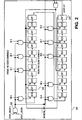
- Fig. 2 illustrates a circuit diagram 200 utilized by an embodiment of the present invention.
- circuit 200 is a gate level implementation of a single MISR from block diagram 100.
- a MISR(n)_rst_in signal initializes the MISR and is a first step to enable data capture.
- a logical AND gate 202 receives an enable signal, MISR_ENABLE, and the Test Mode signal.
- the AND gate 202 is replaced by a multiplexer.
- the logical AND gate 202 enables the MISR's data capture feature and requires that both the MISR_ENABLE and Test Mode signal are a logic high, "1". Proceeding on, the MISR captures data into the plurality of flip flops 220-230 from the scan chains, specifically, from a plurality of signals, in0, in1, in2, in3, in4, in5, in6, in7, and in8.
- the plurality of XOR gates and flip flops(SFF) allow for an analysis of the polynomial received from the outputs of the scan chain, in0-in8.
- the polynomial can be divided and the remainder analyzed to determine if there is a match with a signature. Based on simulation results, the signature indicates whether the device is properly functioning or is a defective integrated device.
- the plurality of XOR gates and flip-flops receive the signature and analyze it.
- the multiple possibilities of designing a gate level implementation of the MISR based on design constraints such as silicon die size, power requirements, polynomial specification, and design functionality specifications.
- the size of the polynomial can be increased or decreased based on the number of input signals in0-in8.
- the MISRs 116-118 each can have a separate clock or a global clock to disable the input capture capability.
- the logical AND gate 202 can be replaced with a multiplexer. Also, one can address the issue of aliasing by increasing the length of the MISR, which has the effect of minimizing the aliasing effect.
- the circuit diagram 200 is in the data capture mode as previously discussed when the MISR has been initialized by pulsing MISR(n)_rst_in signal and the output of the AND gate 202 is a logic high. However, if a value from an un-initialized node propagates to the MISR input, the MISR data capture is disabled by setting the MISR_ENABLE signal to a logic zero, "0", for the clock cycle during which the value of the un-initialized node would have been captured in the MISR. In one embodiment, the clock cycle during which the value of the un-initialized node would have been captured, is determined by logic simulation software.
- the MISR will be disabled from receiving an input one clock cycle before the un-initialized value is received by the MISR. Proceeding on, once the value of the un-initialized node is replaced with valid data, the date capture is enabled by setting the MISR_ENABLE signal to a logic one, "1".
- MISR_ENABLE signal a logic one, "1"
- Fig. 2 enables generating signatures despite the presence of values from un-initialized nodes. Also, since there are a plurality of MISRs, the invention allows for generating signatures if one of the MISRs are disabled. In one embodiment, each MISR receives inputs from the scan chains based on a respective clock domain, wherein the segregation of MISRs based on clock domains will allow generating signatures despite a corrupted clock domain. Thus, the invention allows for a flexible and fault tolerant test signature generation.
- each MISR can receive different numbers of inputs, specifically, MISR 116 can receive 8 inputs, while MISR 118 can receive 16 inputs from the scan chains.
- the invention is capable of supporting multiple variations of gate level implementations of the MISR.
- a MISR with individual clock, reset, and disable controls can be controlled by logic or external pins.
- the plurality of MISRs can be simultaneously reset or disabled by one global signal generated by logic or an external pin.
- the invention can support MISRs with different polynomial sizes by the ability to add more logic and flip flops to store larger polynomials.
Landscapes
- Engineering & Computer Science (AREA)
- General Engineering & Computer Science (AREA)
- Physics & Mathematics (AREA)
- General Physics & Mathematics (AREA)
- Tests Of Electronic Circuits (AREA)
- Test And Diagnosis Of Digital Computers (AREA)
- Semiconductor Integrated Circuits (AREA)
- Testing Of Individual Semiconductor Devices (AREA)
- Testing Electric Properties And Detecting Electric Faults (AREA)
Abstract
Description
- The present invention relates to design for test improvements, and specifically to a method and apparatus for fault tolerant and flexible test signature generator within an integrated device.
- Modem integrated circuit (IC) devices include large numbers of gates on a single semiconductor chip, with these gates interconnected so as to perform multiple and complex functions. The fabrication of an IC incorporating such Very Large Scale Integration (VLSI) must be error free, as a manufacturing defect may prevent the IC from performing all of the functions that an IC is designed to perform. Such demands require verification of the design of the IC and also various types of electrical testing after the IC is manufactured.
- However, as the complexity of the IC increases, so does the cost and complexity of verifying and electrically testing each of the devices in the IC. Electrical testing ensures that each node in a VLSI circuit functions properly. Therefore, each node needs to individually, and in conjunction with the other node in the IC, function properly in all possible combinations of operations. Typically, electrical testing is performed by automated testing equipment (ATE) that employs test vectors to perform the desired tests. A test vector describes the desired test input (or signals), associated clock pulse (or pulses), and expected test output (or signals) for every package pin during a period of time, often in an attempt to "test" a particular node. For complex circuitry, this may involve a large number of test vectors and, accordingly, a long test time.
- One way to address this problem is through design for test (DFT). DFT methods utilize various test circuits. One type of test circuit is a scan path or a scan loop in the logic circuit. A scan path or scan loop comprises of a chain of synchronously clocked master/slave latches (or scan flip flops), each of which is connected to a particular node in the logic circuit. Typical scan circuit designs involve one or more separate scan paths or scan loops. The scan latches can be loaded with a serial data stream of scan vectors that set the logic circuit nodes to a predetermined state. The logic circuit then can be operated in normal fashion and the result of the operation is stored in its respective latch. A scan out operation serially unloads the contents of the latches and the result of the test operation at the associated nodes is analyzed for improper node operation.
- A typical circuit for verifying functionality of the nodes is utilizing a single multiple input signature register (MISR) to receive the outputs of scan chains. Also, additional logic is needed for initializing the integrated device to prevent signature corruption due to un-initialized nodes. However, this requires significant simulation and cost overhead due to the additional logic and design simulation to insure all the nodes are initialized. Also, any scan chain defect adversely impacts the data and signature corruption within the MISR.
- JP 2000352576 (US 6442723) discloses in an LBIST additional built in functions providing dynamically selectable signature generation modes that can be used to isolate und/or diagnose faults.
- US
patent 5 844 917 discloses a method for testing an adapter card comprising an application specific integrated circuit (ASIC) using a reconfigurable logic with the features according to the preamble ofclaim 1. - US
patent 6 199 184 discloses a parallel signature compression circuit including two or more multiple input signature registers (MISRs). The signature registers comprise flip flops. - US
patent 5 930 270 discloses a method for diagnosing the faults of an electronic device. The test results are accumulated into a multiple input shift register (MISR) which can be reset by a global signal. - WO 01/33237 discloses a method and an apparatus for testing a circuit having two or more clock domains under control of a main test clock signal. The method comprises configuring memory elements in a scan mode in which the memory elements are connected to define one or more scan chains in each domain.
- The present invention is illustrated by way of example and not limitation in the following figures. Like references indicate similar elements, in which:
- Fig. 1 illustrates a block diagram utilized by an embodiment of the present invention.
- Fig. 2 illustrates a circuit diagram utilized by an embodiment of the present invention.
- A method and apparatus for fault tolerant and flexible test signature generator within an integrated device are discussed. In the following description, for purposes of explanation, numerous details are set forth in order to provide a thorough understanding of the present invention. However, it will be apparent to one skilled in the art that these specific details are not required in order to practice the present invention.
- Fig. 1 illustrates a block diagram 100 utilized by an embodiment of the present invention. The block diagram 100 comprises a linear feedback shift register 102 (LFSR), a plurality of multiplexers 104-108 which individually select the input to a plurality of scan chains 110-114, and a plurality of multiple input signature registers 116-118 (MISR) is coupled to outputs of the plurality of scan chains. In one embodiment, each MISR is coupled to the output of each scan chain 110-114. In one embodiment, the MISRs 116-118 receive reset controls and are independently reset, which is discussed further in Fig. 2. In another embodiment, the MISRs 116-118 are simultaneously reset by a global reset signal or enabled by a global enable signal.
- The LFSR 102 generates test patterns, which in one embodiment are forwarded to the plurality of scan chains via the multiplexers 104-108. In another embodiment, the test patterns from the LFSR are forwarded to the plurality of scan chains without the need for multiplexers 104-108. For the embodiment with the multiplexers 104-108, one example of the operation is the
multiplexer 104 selects either the scan input signal SI_0 or the input fromLFSR 102 and forwards the input to thescan chain 110. A control signal, Test Mode, instructs the multiplexer on which input to forward to the scan chain. In one embodiment, the Test Mode signal is alogic 1 and enables a logic built in self test mode (LBIST). If the Test Mode signal is alogic 1, themultiplexer 104 selects the LFSR 102 input to forward to thescan chain 110. The MISRs 116-118 receive inputs from the outputs of the plurality of scan chains 110-114 and are discussed further in Fig. 2. In one embodiment, the contents of the MISR are forwarded to automatic test equipment (ATE) in order to compare the expected test pattern results to the actual test pattern results stored in the MISR. In one embodiment, Fig. 1 resides on a single integrated device. - Fig. 2 illustrates a circuit diagram 200 utilized by an embodiment of the present invention. In one embodiment,
circuit 200 is a gate level implementation of a single MISR from block diagram 100. A MISR(n)_rst_in signal initializes the MISR and is a first step to enable data capture. In one embodiment, a logical ANDgate 202 receives an enable signal, MISR_ENABLE, and the Test Mode signal. In another example, the ANDgate 202 is replaced by a multiplexer. For the embodiment with thelogical AND gate 202, after the MISR is initialized by pulsing the MISR(n)_rst_in signal, the logical ANDgate 202 enables the MISR's data capture feature and requires that both the MISR_ENABLE and Test Mode signal are a logic high, "1". Proceeding on, the MISR captures data into the plurality of flip flops 220-230 from the scan chains, specifically, from a plurality of signals, in0, in1, in2, in3, in4, in5, in6, in7, and in8. The plurality of XOR gates and flip flops(SFF) allow for an analysis of the polynomial received from the outputs of the scan chain, in0-in8. For example, the polynomial can be divided and the remainder analyzed to determine if there is a match with a signature. Based on simulation results, the signature indicates whether the device is properly functioning or is a defective integrated device. The plurality of XOR gates and flip-flops receive the signature and analyze it. - One skilled in the art appreciates the multiple possibilities of designing a gate level implementation of the MISR based on design constraints such as silicon die size, power requirements, polynomial specification, and design functionality specifications. For example, the size of the polynomial can be increased or decreased based on the number of input signals in0-in8. Also, the MISRs 116-118 each can have a separate clock or a global clock to disable the input capture capability. The logical AND
gate 202 can be replaced with a multiplexer. Also, one can address the issue of aliasing by increasing the length of the MISR, which has the effect of minimizing the aliasing effect. - The circuit diagram 200 is in the data capture mode as previously discussed when the MISR has been initialized by pulsing MISR(n)_rst_in signal and the output of the AND
gate 202 is a logic high. However, if a value from an un-initialized node propagates to the MISR input, the MISR data capture is disabled by setting the MISR_ENABLE signal to a logic zero, "0", for the clock cycle during which the value of the un-initialized node would have been captured in the MISR. In one embodiment, the clock cycle during which the value of the un-initialized node would have been captured, is determined by logic simulation software. Once the clock cycle of the un-initialized node has been determined, the MISR will be disabled from receiving an input one clock cycle before the un-initialized value is received by the MISR. Proceeding on, once the value of the un-initialized node is replaced with valid data, the date capture is enabled by setting the MISR_ENABLE signal to a logic one, "1". Thus, each MISR depicted in Fig. I can be independently controlled and reset. - Fig. 2 enables generating signatures despite the presence of values from un-initialized nodes. Also, since there are a plurality of MISRs, the invention allows for generating signatures if one of the MISRs are disabled. In one embodiment, each MISR receives inputs from the scan chains based on a respective clock domain, wherein the segregation of MISRs based on clock domains will allow generating signatures despite a corrupted clock domain. Thus, the invention allows for a flexible and fault tolerant test signature generation.
- One skilled in the art would appreciate utilizing various embodiments. For example, each MISR can receive different numbers of inputs, specifically,
MISR 116 can receive 8 inputs, whileMISR 118 can receive 16 inputs from the scan chains. The invention is capable of supporting multiple variations of gate level implementations of the MISR. For example, a MISR with individual clock, reset, and disable controls can be controlled by logic or external pins. In contrast, the plurality of MISRs can be simultaneously reset or disabled by one global signal generated by logic or an external pin. Also, the invention can support MISRs with different polynomial sizes by the ability to add more logic and flip flops to store larger polynomials. - While the invention has been described with reference to specific modes and embodiments, for ease of explanation and understanding, those skilled in the art will appreciate that the invention is not necessarily limited to the particular features shown herein, and that the invention may be practiced in a variety of ways that fall under the scope of the claims that follow.
Claims (8)
- An apparatus comprising:a generator (102) to generate a pattern;a plurality of scan chains (110, 112, 114) to receive the pattern from the generator (102);anda plurality of independently reset and enabled signature registers (116, 118) coupled to the plurality of scan chains (110, 112, 114), to receive an output of at least one of the plurality of scan chains (110, 112, 114) during a mode of an integrated device, characterized in that the plurality of signature registers (116, 118) is to be simultaneously reset by a global signal and at least one signature register is to be disabled one clock cycle before a detection of an un-initialized node by the signature register, and the signature register is to be enabled once the value of the un-initialized logic node is replaced with a valid data.
- The apparatus of claim 1 further comprising a plurality of multiplexers (104, 106, 108) coupled to the generator (102) and plurality of scan chains (110, 112, 114), to forward the pattern from the generator (102) to the plurality of scan chains (110, 112, 114) in response to a signal.
- The apparatus of claim 2 wherein the signal is a built in self test activation.
- The apparatus of claim 1 wherein the signature register (116, 118) comprises a plurality of flip flops (220, 230) to receive the output of the scan chains (110, 112, 114).
- The apparatus of claim 1 wherein the mode of the integrated device is a state with at least one un-initialized logic node.
- An integrated device comprising the apparatus of claim 1.
- The integrated device of claim 6 further comprising a plurality of multiplexers (104, 106, 108) coupled to the generator (102) and plurality of scan chains (110, 112, 114), to forward the pattern from the generator (102) to the plurality of scan chains (110, 112, 114) in response to a signal.
- The integrated device of claim 7 wherein the signal is a built in self test activation.
Applications Claiming Priority (3)
| Application Number | Priority Date | Filing Date | Title |
|---|---|---|---|
| US862407 | 2001-05-21 | ||
| US09/862,407 US6738939B2 (en) | 2001-05-21 | 2001-05-21 | Method and apparatus for fault tolerant and flexible test signature generator |
| PCT/US2002/015806 WO2002095587A2 (en) | 2001-05-21 | 2002-05-16 | Method and apparatus for fault tolerant and flexible test signature generator |
Publications (2)
| Publication Number | Publication Date |
|---|---|
| EP1393176A2 EP1393176A2 (en) | 2004-03-03 |
| EP1393176B1 true EP1393176B1 (en) | 2006-11-08 |
Family
ID=25338422
Family Applications (1)
| Application Number | Title | Priority Date | Filing Date |
|---|---|---|---|
| EP02731860A Expired - Lifetime EP1393176B1 (en) | 2001-05-21 | 2002-05-16 | Method and apparatus for fault tolerant and flexible test signature generator |
Country Status (8)
| Country | Link |
|---|---|
| US (1) | US6738939B2 (en) |
| EP (1) | EP1393176B1 (en) |
| CN (1) | CN1329833C (en) |
| AT (1) | ATE344943T1 (en) |
| AU (1) | AU2002303801A1 (en) |
| DE (1) | DE60215933T2 (en) |
| TW (1) | TWI230795B (en) |
| WO (1) | WO2002095587A2 (en) |
Families Citing this family (24)
| Publication number | Priority date | Publication date | Assignee | Title |
|---|---|---|---|---|
| US6996760B2 (en) * | 2001-10-12 | 2006-02-07 | Sun Microsystems | ASIC BIST employing stored indications of completion |
| US6981191B2 (en) * | 2001-10-12 | 2005-12-27 | Sun Microsystems, Inc. | ASIC logic BIST employing registers seeded with differing primitive polynomials |
| US7644333B2 (en) * | 2001-12-18 | 2010-01-05 | Christopher John Hill | Restartable logic BIST controller |
| US6918074B2 (en) * | 2002-06-28 | 2005-07-12 | Intel Corporation | At speed testing asynchronous signals |
| CN1516015B (en) * | 2003-01-09 | 2010-04-07 | 华为技术有限公司 | Multi-chain boundary scan test system and multi-chain boundary scan test method |
| US20040139377A1 (en) * | 2003-01-13 | 2004-07-15 | International Business Machines Corporation | Method and apparatus for compact scan testing |
| CN100348992C (en) * | 2003-11-19 | 2007-11-14 | 华为技术有限公司 | Testing method of peripheral interconnecting wire |
| CN100370269C (en) * | 2003-11-19 | 2008-02-20 | 华为技术有限公司 | A boundary scan test controller and a boundary scan test method |
| US6972592B2 (en) * | 2003-11-24 | 2005-12-06 | Lsi Logic Corporation | Self-timed scan circuit for ASIC fault testing |
| DE102005046588B4 (en) * | 2005-09-28 | 2016-09-22 | Infineon Technologies Ag | Apparatus and method for testing and diagnosing digital circuits |
| US7996731B2 (en) | 2005-11-02 | 2011-08-09 | Advanced Micro Devices, Inc. | Error detection in high-speed asymmetric interfaces |
| US7415678B2 (en) * | 2005-11-15 | 2008-08-19 | Synopsys, Inc. | Method and apparatus for synthesis of multimode X-tolerant compressor |
| US20090228751A1 (en) * | 2007-05-22 | 2009-09-10 | Tilman Gloekler | method for performing logic built-in-self-test cycles on a semiconductor chip and a corresponding semiconductor chip with a test engine |
| US7882409B2 (en) * | 2007-09-21 | 2011-02-01 | Synopsys, Inc. | Method and apparatus for synthesis of augmented multimode compactors |
| US7949921B2 (en) * | 2007-09-21 | 2011-05-24 | Synopsys, Inc. | Method and apparatus for synthesis of augmented multimode compactors |
| US8365029B2 (en) * | 2007-12-26 | 2013-01-29 | Infineon Technologies Ag | Digital circuits and methods for testing a digital circuit |
| US20090265596A1 (en) * | 2008-04-22 | 2009-10-22 | Mediatek Inc. | Semiconductor devices, integrated circuit packages and testing methods thereof |
| US8949493B1 (en) | 2010-07-30 | 2015-02-03 | Altera Corporation | Configurable multi-lane scrambler for flexible protocol support |
| US10345369B2 (en) | 2012-10-02 | 2019-07-09 | Synopsys, Inc. | Augmented power-aware decompressor |
| EP3153873A1 (en) * | 2015-10-07 | 2017-04-12 | Lantiq Beteiligungs-GmbH & Co. KG | On-chip test pattern generation |
| US10380303B2 (en) | 2015-11-30 | 2019-08-13 | Synopsys, Inc. | Power-aware dynamic encoding |
| US10079070B2 (en) * | 2016-10-20 | 2018-09-18 | International Business Machines Corporation | Testing content addressable memory and random access memory |
| US10509072B2 (en) * | 2017-03-03 | 2019-12-17 | Mentor Graphics Corporation | Test application time reduction using capture-per-cycle test points |
| US12412014B1 (en) * | 2022-08-31 | 2025-09-09 | Cadence Design Systems, Inc. | IC chip with IC design modification detection |
Family Cites Families (16)
| Publication number | Priority date | Publication date | Assignee | Title |
|---|---|---|---|---|
| US4503537A (en) * | 1982-11-08 | 1985-03-05 | International Business Machines Corporation | Parallel path self-testing system |
| US5331643A (en) * | 1991-09-04 | 1994-07-19 | International Business Machines Corporation | Self-testing logic with embedded arrays |
| US5329533A (en) * | 1991-12-26 | 1994-07-12 | At&T Bell Laboratories | Partial-scan built-in self-test technique |
| EP0642083A1 (en) * | 1993-09-04 | 1995-03-08 | International Business Machines Corporation | Test circuit and method for interconnect testing of chips |
| US5991909A (en) | 1996-10-15 | 1999-11-23 | Mentor Graphics Corporation | Parallel decompressor and related methods and apparatuses |
| US5790561A (en) * | 1997-01-17 | 1998-08-04 | Rockwell International Corporation | Internal testability system for microprocessor-based integrated circuit |
| US5844917A (en) | 1997-04-08 | 1998-12-01 | International Business Machines Corporation | Method for testing adapter card ASIC using reconfigurable logic |
| US5930270A (en) | 1997-07-23 | 1999-07-27 | International Business Machines Corporation | Logic built in self-test diagnostic method |
| KR100292821B1 (en) * | 1997-09-08 | 2001-06-15 | 윤종용 | Parallel Signature Compression Circuit |
| US6049901A (en) * | 1997-09-16 | 2000-04-11 | Stock; Mary C. | Test system for integrated circuits using a single memory for both the parallel and scan modes of testing |
| US6021514A (en) * | 1998-01-22 | 2000-02-01 | International Business Machines Corporation | Limited latch linehold capability for LBIST testing |
| US6442723B1 (en) | 1999-05-12 | 2002-08-27 | International Business Machines Corporation | Logic built-in self test selective signature generation |
| US6496503B1 (en) * | 1999-06-01 | 2002-12-17 | Intel Corporation | Device initialization and operation using directed routing |
| US6442722B1 (en) | 1999-10-29 | 2002-08-27 | Logicvision, Inc. | Method and apparatus for testing circuits with multiple clocks |
| US6557129B1 (en) * | 1999-11-23 | 2003-04-29 | Janusz Rajski | Method and apparatus for selectively compacting test responses |
| US6516432B1 (en) * | 1999-12-22 | 2003-02-04 | International Business Machines Corporation | AC scan diagnostic method |
-
2001
- 2001-05-21 US US09/862,407 patent/US6738939B2/en not_active Expired - Lifetime
-
2002
- 2002-03-13 TW TW091104698A patent/TWI230795B/en not_active IP Right Cessation
- 2002-05-16 CN CNB028099745A patent/CN1329833C/en not_active Expired - Fee Related
- 2002-05-16 EP EP02731860A patent/EP1393176B1/en not_active Expired - Lifetime
- 2002-05-16 AU AU2002303801A patent/AU2002303801A1/en not_active Abandoned
- 2002-05-16 DE DE60215933T patent/DE60215933T2/en not_active Expired - Fee Related
- 2002-05-16 AT AT02731860T patent/ATE344943T1/en not_active IP Right Cessation
- 2002-05-16 WO PCT/US2002/015806 patent/WO2002095587A2/en not_active Ceased
Also Published As
| Publication number | Publication date |
|---|---|
| DE60215933T2 (en) | 2007-04-26 |
| WO2002095587A3 (en) | 2003-08-28 |
| WO2002095587A2 (en) | 2002-11-28 |
| TWI230795B (en) | 2005-04-11 |
| AU2002303801A1 (en) | 2002-12-03 |
| ATE344943T1 (en) | 2006-11-15 |
| CN1329833C (en) | 2007-08-01 |
| US20020174393A1 (en) | 2002-11-21 |
| DE60215933D1 (en) | 2006-12-21 |
| EP1393176A2 (en) | 2004-03-03 |
| US6738939B2 (en) | 2004-05-18 |
| CN1529855A (en) | 2004-09-15 |
Similar Documents
| Publication | Publication Date | Title |
|---|---|---|
| US6738939B2 (en) | Method and apparatus for fault tolerant and flexible test signature generator | |
| EP0880708B1 (en) | I/o toggle test method using jtag | |
| US7644333B2 (en) | Restartable logic BIST controller | |
| US6701476B2 (en) | Test access mechanism for supporting a configurable built-in self-test circuit and method thereof | |
| US7080301B2 (en) | On-chip service processor | |
| US5383143A (en) | Self re-seeding linear feedback shift register (LFSR) data processing system for generating a pseudo-random test bit stream and method of operation | |
| US6314539B1 (en) | Boundary-scan register cell with bypass circuit | |
| US7774662B2 (en) | Method and structure for picosecond-imaging-circuit-analysis based built-in-self-test diagnostic | |
| JP3749541B2 (en) | Integrated circuit test apparatus and test method | |
| US8898529B2 (en) | High performance compaction for test responses with many unknowns | |
| US20160011260A1 (en) | On-Chip Service Processor | |
| US5805609A (en) | Method and apparatus for testing a megacell in an ASIC using JTAG | |
| US8671320B2 (en) | Integrated circuit comprising scan test circuitry with controllable number of capture pulses | |
| US20090217116A1 (en) | Diagnosable general purpose test registers scan chain design | |
| CN114667455B (en) | Universal compressor architecture for test circuits | |
| US6029261A (en) | Test circuit and system for interconnect testing of high-level packages | |
| US5150366A (en) | Reduced delay circuits for shift register latch scan strings | |
| US6446229B1 (en) | Method and apparatus for integrated flip-flop to support two test modes | |
| Lala | An introduction to logic circuit testing | |
| US10302700B2 (en) | Test circuit to debug missed test clock pulses | |
| US6754867B2 (en) | Method of determining non-accessible device I/O pin speed using on chip LFSR and MISR as data source and results analyzer respectively | |
| CN116741751A (en) | Integrated circuit unit, integrated circuit and die testing methods | |
| US6650136B2 (en) | Method and apparatus to enhance testability of logic coupled to IO buffers | |
| WO2003067274A2 (en) | Method and device for detecting faults on integrated circuits | |
| JP2005017067A (en) | Semiconductor integrated circuit with built-in self-test circuit and fault diagnosis method thereof |
Legal Events
| Date | Code | Title | Description |
|---|---|---|---|
| PUAI | Public reference made under article 153(3) epc to a published international application that has entered the european phase |
Free format text: ORIGINAL CODE: 0009012 |
|
| 17P | Request for examination filed |
Effective date: 20031014 |
|
| AK | Designated contracting states |
Kind code of ref document: A2 Designated state(s): AT BE CH CY DE DK ES FI FR GB GR IE IT LI LU MC NL PT SE TR |
|
| AX | Request for extension of the european patent |
Extension state: AL LT LV MK RO SI |
|
| GRAP | Despatch of communication of intention to grant a patent |
Free format text: ORIGINAL CODE: EPIDOSNIGR1 |
|
| GRAS | Grant fee paid |
Free format text: ORIGINAL CODE: EPIDOSNIGR3 |
|
| GRAA | (expected) grant |
Free format text: ORIGINAL CODE: 0009210 |
|
| AK | Designated contracting states |
Kind code of ref document: B1 Designated state(s): AT BE CH CY DE DK ES FI FR GB GR IE IT LI LU MC NL PT SE TR |
|
| PG25 | Lapsed in a contracting state [announced via postgrant information from national office to epo] |
Ref country code: IT Free format text: LAPSE BECAUSE OF FAILURE TO SUBMIT A TRANSLATION OF THE DESCRIPTION OR TO PAY THE FEE WITHIN THE PRESCRIBED TIME-LIMIT;WARNING: LAPSES OF ITALIAN PATENTS WITH EFFECTIVE DATE BEFORE 2007 MAY HAVE OCCURRED AT ANY TIME BEFORE 2007. THE CORRECT EFFECTIVE DATE MAY BE DIFFERENT FROM THE ONE RECORDED. Effective date: 20061108 Ref country code: AT Free format text: LAPSE BECAUSE OF FAILURE TO SUBMIT A TRANSLATION OF THE DESCRIPTION OR TO PAY THE FEE WITHIN THE PRESCRIBED TIME-LIMIT Effective date: 20061108 Ref country code: LI Free format text: LAPSE BECAUSE OF FAILURE TO SUBMIT A TRANSLATION OF THE DESCRIPTION OR TO PAY THE FEE WITHIN THE PRESCRIBED TIME-LIMIT Effective date: 20061108 Ref country code: CH Free format text: LAPSE BECAUSE OF FAILURE TO SUBMIT A TRANSLATION OF THE DESCRIPTION OR TO PAY THE FEE WITHIN THE PRESCRIBED TIME-LIMIT Effective date: 20061108 Ref country code: BE Free format text: LAPSE BECAUSE OF FAILURE TO SUBMIT A TRANSLATION OF THE DESCRIPTION OR TO PAY THE FEE WITHIN THE PRESCRIBED TIME-LIMIT Effective date: 20061108 Ref country code: FI Free format text: LAPSE BECAUSE OF FAILURE TO SUBMIT A TRANSLATION OF THE DESCRIPTION OR TO PAY THE FEE WITHIN THE PRESCRIBED TIME-LIMIT Effective date: 20061108 |
|
| REG | Reference to a national code |
Ref country code: GB Ref legal event code: FG4D |
|
| REG | Reference to a national code |
Ref country code: CH Ref legal event code: EP |
|
| REG | Reference to a national code |
Ref country code: IE Ref legal event code: FG4D |
|
| REF | Corresponds to: |
Ref document number: 60215933 Country of ref document: DE Date of ref document: 20061221 Kind code of ref document: P |
|
| PG25 | Lapsed in a contracting state [announced via postgrant information from national office to epo] |
Ref country code: DK Free format text: LAPSE BECAUSE OF FAILURE TO SUBMIT A TRANSLATION OF THE DESCRIPTION OR TO PAY THE FEE WITHIN THE PRESCRIBED TIME-LIMIT Effective date: 20070208 Ref country code: SE Free format text: LAPSE BECAUSE OF FAILURE TO SUBMIT A TRANSLATION OF THE DESCRIPTION OR TO PAY THE FEE WITHIN THE PRESCRIBED TIME-LIMIT Effective date: 20070208 |
|
| PG25 | Lapsed in a contracting state [announced via postgrant information from national office to epo] |
Ref country code: ES Free format text: LAPSE BECAUSE OF FAILURE TO SUBMIT A TRANSLATION OF THE DESCRIPTION OR TO PAY THE FEE WITHIN THE PRESCRIBED TIME-LIMIT Effective date: 20070219 |
|
| PG25 | Lapsed in a contracting state [announced via postgrant information from national office to epo] |
Ref country code: PT Free format text: LAPSE BECAUSE OF FAILURE TO SUBMIT A TRANSLATION OF THE DESCRIPTION OR TO PAY THE FEE WITHIN THE PRESCRIBED TIME-LIMIT Effective date: 20070409 |
|
| REG | Reference to a national code |
Ref country code: CH Ref legal event code: PL |
|
| EN | Fr: translation not filed | ||
| PLBE | No opposition filed within time limit |
Free format text: ORIGINAL CODE: 0009261 |
|
| STAA | Information on the status of an ep patent application or granted ep patent |
Free format text: STATUS: NO OPPOSITION FILED WITHIN TIME LIMIT |
|
| 26N | No opposition filed |
Effective date: 20070809 |
|
| PG25 | Lapsed in a contracting state [announced via postgrant information from national office to epo] |
Ref country code: MC Free format text: LAPSE BECAUSE OF NON-PAYMENT OF DUE FEES Effective date: 20070531 |
|
| PG25 | Lapsed in a contracting state [announced via postgrant information from national office to epo] |
Ref country code: FR Free format text: LAPSE BECAUSE OF FAILURE TO SUBMIT A TRANSLATION OF THE DESCRIPTION OR TO PAY THE FEE WITHIN THE PRESCRIBED TIME-LIMIT Effective date: 20070622 Ref country code: GR Free format text: LAPSE BECAUSE OF FAILURE TO SUBMIT A TRANSLATION OF THE DESCRIPTION OR TO PAY THE FEE WITHIN THE PRESCRIBED TIME-LIMIT Effective date: 20070209 |
|
| PG25 | Lapsed in a contracting state [announced via postgrant information from national office to epo] |
Ref country code: IE Free format text: LAPSE BECAUSE OF NON-PAYMENT OF DUE FEES Effective date: 20070516 |
|
| PG25 | Lapsed in a contracting state [announced via postgrant information from national office to epo] |
Ref country code: FR Free format text: LAPSE BECAUSE OF FAILURE TO SUBMIT A TRANSLATION OF THE DESCRIPTION OR TO PAY THE FEE WITHIN THE PRESCRIBED TIME-LIMIT Effective date: 20061108 |
|
| PGFP | Annual fee paid to national office [announced via postgrant information from national office to epo] |
Ref country code: NL Payment date: 20090504 Year of fee payment: 8 |
|
| PG25 | Lapsed in a contracting state [announced via postgrant information from national office to epo] |
Ref country code: LU Free format text: LAPSE BECAUSE OF NON-PAYMENT OF DUE FEES Effective date: 20070516 Ref country code: CY Free format text: LAPSE BECAUSE OF FAILURE TO SUBMIT A TRANSLATION OF THE DESCRIPTION OR TO PAY THE FEE WITHIN THE PRESCRIBED TIME-LIMIT Effective date: 20061108 |
|
| PGFP | Annual fee paid to national office [announced via postgrant information from national office to epo] |
Ref country code: DE Payment date: 20090514 Year of fee payment: 8 |
|
| PG25 | Lapsed in a contracting state [announced via postgrant information from national office to epo] |
Ref country code: TR Free format text: LAPSE BECAUSE OF FAILURE TO SUBMIT A TRANSLATION OF THE DESCRIPTION OR TO PAY THE FEE WITHIN THE PRESCRIBED TIME-LIMIT Effective date: 20061108 |
|
| PGFP | Annual fee paid to national office [announced via postgrant information from national office to epo] |
Ref country code: GB Payment date: 20090513 Year of fee payment: 8 |
|
| REG | Reference to a national code |
Ref country code: NL Ref legal event code: V1 Effective date: 20101201 |
|
| GBPC | Gb: european patent ceased through non-payment of renewal fee |
Effective date: 20100516 |
|
| PG25 | Lapsed in a contracting state [announced via postgrant information from national office to epo] |
Ref country code: NL Free format text: LAPSE BECAUSE OF NON-PAYMENT OF DUE FEES Effective date: 20101201 |
|
| PG25 | Lapsed in a contracting state [announced via postgrant information from national office to epo] |
Ref country code: DE Free format text: LAPSE BECAUSE OF NON-PAYMENT OF DUE FEES Effective date: 20101201 |
|
| PG25 | Lapsed in a contracting state [announced via postgrant information from national office to epo] |
Ref country code: GB Free format text: LAPSE BECAUSE OF NON-PAYMENT OF DUE FEES Effective date: 20100516 |