EP1391760A2 - Optical fiber with antireflection coating, and method for manufacturing the same - Google Patents
Optical fiber with antireflection coating, and method for manufacturing the same Download PDFInfo
- Publication number
- EP1391760A2 EP1391760A2 EP03017715A EP03017715A EP1391760A2 EP 1391760 A2 EP1391760 A2 EP 1391760A2 EP 03017715 A EP03017715 A EP 03017715A EP 03017715 A EP03017715 A EP 03017715A EP 1391760 A2 EP1391760 A2 EP 1391760A2
- Authority
- EP
- European Patent Office
- Prior art keywords
- optical fiber
- antireflection film
- end surface
- coating solution
- film
- Prior art date
- Legal status (The legal status is an assumption and is not a legal conclusion. Google has not performed a legal analysis and makes no representation as to the accuracy of the status listed.)
- Granted
Links
Images


Classifications
-
- G—PHYSICS
- G02—OPTICS
- G02B—OPTICAL ELEMENTS, SYSTEMS OR APPARATUS
- G02B6/00—Light guides; Structural details of arrangements comprising light guides and other optical elements, e.g. couplings
- G02B6/24—Coupling light guides
- G02B6/241—Light guide terminations
-
- G—PHYSICS
- G02—OPTICS
- G02B—OPTICAL ELEMENTS, SYSTEMS OR APPARATUS
- G02B6/00—Light guides; Structural details of arrangements comprising light guides and other optical elements, e.g. couplings
- G02B6/24—Coupling light guides
- G02B6/42—Coupling light guides with opto-electronic elements
- G02B6/4201—Packages, e.g. shape, construction, internal or external details
- G02B6/4202—Packages, e.g. shape, construction, internal or external details for coupling an active element with fibres without intermediate optical elements, e.g. fibres with plane ends, fibres with shaped ends, bundles
- G02B6/4203—Optical features
-
- G—PHYSICS
- G02—OPTICS
- G02B—OPTICAL ELEMENTS, SYSTEMS OR APPARATUS
- G02B6/00—Light guides; Structural details of arrangements comprising light guides and other optical elements, e.g. couplings
- G02B6/24—Coupling light guides
- G02B6/42—Coupling light guides with opto-electronic elements
- G02B6/4201—Packages, e.g. shape, construction, internal or external details
- G02B6/4204—Packages, e.g. shape, construction, internal or external details the coupling comprising intermediate optical elements, e.g. lenses, holograms
- G02B6/4207—Packages, e.g. shape, construction, internal or external details the coupling comprising intermediate optical elements, e.g. lenses, holograms with optical elements reducing the sensitivity to optical feedback
Definitions
- the present invention relates to a method for forming an antireflection coating or film (referred also to as AR coat) on the end surface of an optical fiber, and an optical fiber manufactured according to this method.
- AR coat an antireflection coating or film
- a transparent fluororesin soluble to solvent for example, "CYTOP" produced by ASAHI GLASS CO., LTD.
- CYTOP produced by ASAHI GLASS CO., LTD.
- a desired film thickness can be obtained by controlling the concentration of the fluorine resin solution and the pulling speed.
- Japanese Patent Laid-Open No.58-223639 Japanese Patent Laid-Open No.7-157338
- Japanese Patent Publication No.6-85011 the technique of applying an antireflection film to the end surface of an optical fiber by subjecting the end surface to sputtering treatment or vacuum evaporation has been also widely known.
- the sputtering treatment or vacuum evaporation requires a large film forming device, which leads to an extremely high manufacturing cost. Therefore, a method capable of forming the film at a low cost and an optical fiber manufactured by use of this method have been desired for a long time.
- the present invention has an object to provide an antireflection film forming method for optical surface end surface of an optical fiber allowing even a beginner to easily form an antireflection film at a low cost, and an optical fiber manufactured according to this method.
- an antireflection film forming method for optical surface end surface of an optical fiber allows even a beginner to easily form an antireflection film at a low cost.
- An optical fiber manufactured according to this method is provided.
- the present invention relates to improvements in the optical fiber having an antireflection film formed on the end surface and the antireflection film forming method for optical fiber.
- the end surface of the optical fiber is dipped in a coating solution having a film forming material dissolved therein, and the optical fiber is then pulled up from the coating solution.
- the pulling speed in the pulling is changed to control the film thickness or surface shape to a desired one, and the antireflection film is formed.
- the reflection reducing wavelength band or reflectance is adjusted to a desired one.
- the film forming material is preferably a fluorine-containing compound.
- the end surface of the optical fiber is preferably inclined at a prescribed angle to the level of the coating solution to precisely ensure the desired reflection reducing wavelength band (or desired film thickness) and reflectance, thereby forming an antireflection film.
- the antireflection film on the end surface of the optical filter by dipping method.
- at least the vicinity of the end surface of the optical fiber is dipped in a solvent having the film forming material dissolved therein, and then pulled up from the coating solution.
- the pulling speed is preferably changed to a prescribed value to precisely ensure the desired reflection reducing wavelength band (or desired film thickness) and reflectance, thereby forming an antireflection film.
- the angular inclination between the level of the coating solution and the end surface of the optical fiber is preferably set to, for example, an angle larger than 0° to an angle of 90°.
- the end surface of the optical fiber can be inclined at a prescribed angle to the level of the coating solution and pulled up at a prescribed speed, an antireflection film having desired thickness and reflectance can be easily formed on the end surface of the optical fiber at a low cost.
- the present invention further has the effect that the film thickness, reflectance and the like can be precisely controlled.
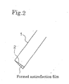
- a typical example of an optical fiber according to the present invention is an optical fiber 1 made of quartz, acryl or the like.
- Such an optical fiber is used, for example, in laser treatment equipment, a survey machine, other fiber arrays, an optical waveguide, or the like.
- An end surface 2 of the optical fiber 1 is dipped in a coating solution 3 in a vessel 5 for a prescribed time, as shown in Figs. 1A-1C, by a pulling device (not shown), and then gradually pulled up while keeping the state where it is inclined at a prescribed angle, for example, 90° (Fig. 1A), 45° (Fig. 1B), or 10° (Fig. 1C), to a level 4 of the coating solution 3.
- a pulling device not shown
- the inclination may be set to an angle ranging from an angle larger than 0° to an angle of 90° without being limited to these angles of 10°, 45°, and 90°, or to other angles.
- the inclination may be 30°.
- the film thickness of the antireflection film to be formed on the end surface of the optical fiber can be gradated from a thin part to a thick part.
- the coating solution 3 is preferably a mixed solvent of 90-99% of an organic solvent having a boiling point of 100 °C to 1-10% of the stock solution of a fluorine-based compound such as a soluble fluororesin produced by ASAHI GLASS CO., LTD. (which also contains a diluent).
- a fluorine-based compound such as a soluble fluororesin produced by ASAHI GLASS CO., LTD. (which also contains a diluent).
- concentration, composition and the like of the coating solution are not limited to the above embodiment, and any concentrations and compositions may be adapted.
- fluororesins produced by AUSIMONT K.K. and DU PONT FLUOROCHEMICAL CO., LTD. can be used, in addition to CYTOP (brand name, produced by ASAHI GLASS CO., LTD.) that is a heat setting type fluorine-based compound of fluorine-containing compounds.
- an ultraviolet curing fluorine acrylic resin an ultraviolet curing fluorine epoxy resin, a heat setting type sol-gel fluorine silicon compound, and a fluorine-containing compound that is a sol-gel material can be also used.
- fluoroalkyl silane is also usable.
- CF 3 CH 2 CH 2 Si(OMe) 3 CF 3 (CF 2 ) 5 CH 2 CH 2 Si(OMe) 3 , CF 3 (CF 2 ) 7 CH 2 CH 2 Si(OMe) 3 , CF 3 (CF 2 ) 7 CH 2 CH 2 SiMe(OMe) 3 , CF 3 CH 2 CH 2 SiCl 3 , CF 3 CH 2 CH 2 Si(OMe) 3 , CF 3 (CF 2 ) 5 CH 2 CH 2 SiCl 3 , CF 3 (CF 2 ) 5 CH 2 CH 2 Si(OMe) 3 , CF 3 (CF 2 ) 7 CH 2 CH 2 SiCl 3 , CF 3 (CF 2 ) 7 CH 2 CH 2 Si(OMe) 3 , CF 3 (CF 2 ) 7 CH 2 CH 2 SiMeCl 2 , CF 3 (CF 2 ) 7 CH 2 CH 2 SiMe(OMe) 2 , CF 3 (CF 2 ) 7 CH 2 CH 2 SiMe(OMe) 2 ,
- the suitable pulling speed is about several mm/min-200 mm/min.
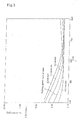
- the antireflection film is preferably formed on the end surface 2 of the optical fiber 1 at a pulling speed of 20.0 mm/min so as to have a film thickness of 0.1 ⁇ m. Further, the antireflection film is preferably formed at a pulling speed of 4.0 mm/min so as to have a film thickness of 0.1 ⁇ m or less.
- Fig. 3 the change in reflectance to the wavelength band of light from 400 nm to 800 nm of the formed antireflection film, when the pulling speed is changed, is shown in detail.
- a monitor glass substrate with a refractive index of 1.50 of the same quality as a quartz optical fiber is used.
- the reflection reducing wavelength band is changed from the relation showing the minimum reflectance (maximum transmittance) in the vicinity of 760 nm to the relation showing the minimum reflectance (maximum transmittance) in the vicinity of 530 nm.
- the reflectance can be changed to change the reflection reducing wavelength range to a short wavelength band.
- the reflectance is 7% in double reflection when no antireflection film (AR coat) is formed, but it can be suppressed to the minimum reflectance in double reflection when the antireflection film (AR coat) is formed.
- the reflection reducing wavelength band can be changed also by changing the concentration of the coating solution.
- the forming method of a single-layer antireflection film of a fluorine-based inorganic silicon compound was described, but in the forming method of a multiplayer antireflection film having a high refractive index material laminated together, the reflectance can be reduced to 0 at the minimum.
- the antireflection film (AR coat) is formed on the end surface of one optical fiber by physical adsorption by dipping method was described above.
- the present invention is not limited by this, and a method for treating a number of optical fibers in large quantities may be adapted.
Landscapes
- Physics & Mathematics (AREA)
- General Physics & Mathematics (AREA)
- Optics & Photonics (AREA)
- Surface Treatment Of Optical Elements (AREA)
- Application Of Or Painting With Fluid Materials (AREA)
- Optical Fibers, Optical Fiber Cores, And Optical Fiber Bundles (AREA)
Abstract
Description
Claims (11)
- Method for forming an antireflection film on an optical fiber characterized by
dipping an optical fiber (1) in a coating solution (3) having a film forming material dissolved therein; and
forming an antireflection film on the end surface (2) of the optical fiber (1). - Method of claim 1, characterized in that the dipped fiber (1) is pulled up from the coating solution (3).
- Method of claim 2. characterized in that the pulling speed is changed, when the optical fiber (1) is pulled up from the coating solution (3), to adjust the reflection reducing wavelength band of the antireflection film to be formed on the end surface (2) of the optical fiber (1).
- Method of claim 2, characterized in that the pulling speed is changed, when the optical fiber (1) is pulled up from the coating solution (3), to adjust the reflectance of the antireflection film to be formed on the end surface (2) of the optical fiber (1).
- Method of anyone of claims 1 through 4, characterized in that the film forming material is a fluorine containing compound.
- Method of anyone of claims 2 through 5, characterized in that the angle of the end surface (2) of the optical fiber (1) to the level (4) of the coating solution (3) is changed, when the optical fiber (1) is pulled up from the coating solution (3), to adjust the reflection reducing wavelength band of the antireflection film to be formed on the end surface (2) of the optical fiber (1).
- Method of anyone of claims 2 through 5, characterized in that the angle of the end surface (2) of the optical fiber (1) to the level (4) of the coating solution (3) is changed, when the optical fiber (1) is pulled up from the coating solution (3), to adjust the reflectance of the antireflection film to be formed on the end surface (2) of the optical fiber (1).
- Optical fiber having an antireflection film formed on the end surface (2), the antireflection film being formed by dipping.
- Optical fiber of claim 8, characterized in that the film forming material is a fluorine-containing compound.
- Optical fiber of claims 8 or 9, characterized in that the film thickness of the antireflection film is uneven.
- Optical fiber of claim 8 or 9, characterized in that the film thickness of the antireflection film is even.
Applications Claiming Priority (2)
| Application Number | Priority Date | Filing Date | Title |
|---|---|---|---|
| JP2002229627 | 2002-08-07 | ||
| JP2002229627A JP2004070033A (en) | 2002-08-07 | 2002-08-07 | Optical fiber having antireflection film formed thereon and method of manufacturing the same |
Publications (3)
| Publication Number | Publication Date |
|---|---|
| EP1391760A2 true EP1391760A2 (en) | 2004-02-25 |
| EP1391760A3 EP1391760A3 (en) | 2004-04-28 |
| EP1391760B1 EP1391760B1 (en) | 2007-06-06 |
Family
ID=31185123
Family Applications (1)
| Application Number | Title | Priority Date | Filing Date |
|---|---|---|---|
| EP03017715A Expired - Lifetime EP1391760B1 (en) | 2002-08-07 | 2003-08-02 | Optical fiber with antireflection coating, and method for manufacturing the same |
Country Status (4)
| Country | Link |
|---|---|
| US (1) | US7201939B2 (en) |
| EP (1) | EP1391760B1 (en) |
| JP (1) | JP2004070033A (en) |
| DE (1) | DE60314208T2 (en) |
Families Citing this family (6)
| Publication number | Priority date | Publication date | Assignee | Title |
|---|---|---|---|---|
| EP2083323A1 (en) * | 2008-01-22 | 2009-07-29 | Lumin Visual Technologies AG | Screen emulsion |
| JP5242208B2 (en) * | 2008-03-21 | 2013-07-24 | 古河電気工業株式会社 | Method of forming reflection end face of optical component and optical component having reflection end face |
| WO2013096886A1 (en) * | 2011-12-22 | 2013-06-27 | Arrayed Fiberoptics Corporation | Non-contact optical fiber connector component |
| US10545294B1 (en) | 2019-07-08 | 2020-01-28 | Arrayed Fiberoptics Corporation | Microfabrication method for optical components |
| CN108609868B (en) * | 2018-07-17 | 2024-04-30 | 四川乐飞光电科技有限公司 | Novel optical fiber coloring curing oven |
| US11333835B2 (en) | 2019-07-08 | 2022-05-17 | Arrayed Fiberoptics Corporation | Microfabrication method for optical components |
Family Cites Families (23)
| Publication number | Priority date | Publication date | Assignee | Title |
|---|---|---|---|---|
| JPS58223693A (en) | 1982-06-16 | 1983-12-26 | Toshiba Corp | Base of gallium phosphide single crystal |
| NL8204961A (en) * | 1982-12-23 | 1984-07-16 | Philips Nv | MONOMODE OPTICAL TRANSMISSION FIBER WITH A TAPER END SECTION AND METHOD FOR MANUFACTURING THE SAME |
| JPS6068319A (en) | 1983-08-23 | 1985-04-18 | Toray Ind Inc | Production of antireflection lens |
| JPH0685011B2 (en) | 1985-08-23 | 1994-10-26 | 旭化成工業株式会社 | Plastic optical fiber terminal processing method |
| JPS6338905A (en) | 1986-08-04 | 1988-02-19 | Toray Ind Inc | Optical fiber having coating film |
| NL8602277A (en) * | 1986-09-10 | 1988-04-05 | Philips Nv | OPTICAL TRANSMISSION FIBER WITH A TAPER END SECTION FITTED WITH A LENS. |
| JPH07119842B2 (en) | 1987-05-28 | 1995-12-20 | セイコーエプソン株式会社 | Optical article having inorganic coating film and method for producing the same |
| JP2613436B2 (en) | 1988-06-10 | 1997-05-28 | 旭光学工業株式会社 | Method of forming antireflection film for plastic lens |
| JP2748413B2 (en) | 1988-07-08 | 1998-05-06 | 旭硝子株式会社 | Low reflection processing agent |
| JPH07157338A (en) | 1993-12-10 | 1995-06-20 | Matsushita Electric Works Ltd | Method for coating optical fiber and end face of optical fiber |
| JPH07294706A (en) | 1994-04-28 | 1995-11-10 | Matsushita Electric Ind Co Ltd | Anti-reflection panel, lens and protective film formation method |
| US6174424B1 (en) * | 1995-11-20 | 2001-01-16 | Cirrex Corp. | Couplers for optical fibers |
| JP3299477B2 (en) * | 1997-02-07 | 2002-07-08 | 光信 宮城 | Manufacturing method of hollow waveguide |
| EP0879991A3 (en) * | 1997-05-13 | 1999-04-21 | Matsushita Electric Industrial Co., Ltd. | Illuminating system |
| CA2361817A1 (en) * | 1999-02-05 | 2000-08-10 | Steven B. Dawes | Optical fiber component with shaped optical element and method of making same |
| US7245647B2 (en) * | 1999-10-28 | 2007-07-17 | Ricoh Company, Ltd. | Surface-emission laser diode operable in the wavelength band of 1.1-1.7mum and optical telecommunication system using such a laser diode |
| JP2001305302A (en) | 2000-04-20 | 2001-10-31 | Asahi Optical Co Ltd | Coating method capable of thickening film and plastic lens |
| JP2002038075A (en) * | 2000-07-11 | 2002-02-06 | Three M Innovative Properties Co | Coating composition for part of optical apparatus or part of electrical apparatus and coating method |
| EP1329745A4 (en) * | 2000-08-29 | 2008-05-21 | Japan Science & Tech Agency | METHOD FOR FORMING THIN OPTICAL FILM |
| JP2002107502A (en) | 2000-09-29 | 2002-04-10 | Seiko Epson Corp | Method for manufacturing optical component, optical component, and electronic device |
| EP1329752B1 (en) * | 2002-10-29 | 2005-02-23 | Agilent Technologies Inc. a Delaware Corporation | Tip for optical waveguide |
| US20050136180A1 (en) * | 2003-12-19 | 2005-06-23 | 3M Innovative Properties Company | Method of coating a substrate with a fluoropolymer |
| JP4344638B2 (en) * | 2004-03-26 | 2009-10-14 | 富士フイルム株式会社 | Antireflection film, manufacturing method thereof, manufacturing apparatus |
-
2002
- 2002-08-07 JP JP2002229627A patent/JP2004070033A/en active Pending
-
2003
- 2003-07-21 US US10/623,154 patent/US7201939B2/en not_active Expired - Fee Related
- 2003-08-02 DE DE60314208T patent/DE60314208T2/en not_active Expired - Fee Related
- 2003-08-02 EP EP03017715A patent/EP1391760B1/en not_active Expired - Lifetime
Also Published As
| Publication number | Publication date |
|---|---|
| DE60314208D1 (en) | 2007-07-19 |
| EP1391760A3 (en) | 2004-04-28 |
| EP1391760B1 (en) | 2007-06-06 |
| JP2004070033A (en) | 2004-03-04 |
| DE60314208T2 (en) | 2008-01-31 |
| US20050079285A1 (en) | 2005-04-14 |
| US7201939B2 (en) | 2007-04-10 |
Similar Documents
| Publication | Publication Date | Title |
|---|---|---|
| US6356694B1 (en) | Process for producing planar waveguide structures as well as waveguide structure | |
| US7542207B2 (en) | Antiglare and antireflection film polarizing plate and display device | |
| US20060074172A1 (en) | Antiglare and antireflection coatings of surface active nanoparticles | |
| US10401536B2 (en) | Item coated with a silicon/organic layer improving the performances of an outer coating | |
| US20170227681A1 (en) | Ophthalmic Lens Comprising a Thin Antireflective Coating with a Very Low Reflection in the Visible Region | |
| US20090053465A1 (en) | Scratch resistant, reflection reducing surface having anti-fogging properties | |
| JPH01114808A (en) | Cladding of light waveguide fiber | |
| CN101639663A (en) | Light-transmitting member, timepiece, and method for manufacturing light-transmitting member | |
| US20080292787A1 (en) | Edging Process of Lens Using Transparent Coating Layer for Protecting Lens | |
| US7201939B2 (en) | Optical fiber with antireflection coating, and method for manufacturing the same | |
| KR20110097791A (en) | Method for manufacturing optical product having anti-glare property | |
| US20180259681A1 (en) | Optical member, image pickup apparatus, and method for manufacturing optical member | |
| JP2001264509A (en) | Article coated with antireflection film and method for producing the same | |
| US20060204197A1 (en) | Optical waveguide and method for preparing the same | |
| US10877182B2 (en) | Optical article comprising a substrate with an antireflective coating | |
| US20120237684A1 (en) | Method of manufacturing a transparent member and plastic member | |
| EP3605155A1 (en) | Ophthalmic lens comprising a multilayered interferential coating and manufacturing method thereof | |
| KR102584462B1 (en) | A Method for Producing a Anti Fingerprinting Coating Lens | |
| JP4926379B2 (en) | Method for producing transparent member having fluoride layer on surface and plastic member | |
| US12535621B2 (en) | Surface coating for optical emitter components | |
| JP4823569B2 (en) | Optical glass component and manufacturing method thereof | |
| JP3180859B2 (en) | Manufacturing method of planar optical waveguide | |
| EP4336226B1 (en) | Method for producing anti-reflective textured surface using additive thin film | |
| RU95121600A (en) | F light guide (OPTIONS), METHOD FOR MANUFACTURING A F light guide and FIBER OPTICAL AMPLIFIER | |
| WO2024204700A1 (en) | Spectacle lens and spectacles |
Legal Events
| Date | Code | Title | Description |
|---|---|---|---|
| PUAI | Public reference made under article 153(3) epc to a published international application that has entered the european phase |
Free format text: ORIGINAL CODE: 0009012 |
|
| AK | Designated contracting states |
Kind code of ref document: A2 Designated state(s): AT BE BG CH CY CZ DE DK EE ES FI FR GB GR HU IE IT LI LU MC NL PT RO SE SI SK TR |
|
| AX | Request for extension of the european patent |
Extension state: AL LT LV MK |
|
| PUAL | Search report despatched |
Free format text: ORIGINAL CODE: 0009013 |
|
| AK | Designated contracting states |
Kind code of ref document: A3 Designated state(s): AT BE BG CH CY CZ DE DK EE ES FI FR GB GR HU IE IT LI LU MC NL PT RO SE SI SK TR |
|
| AX | Request for extension of the european patent |
Extension state: AL LT LV MK |
|
| RIC1 | Information provided on ipc code assigned before grant |
Ipc: 7G 02B 6/42 B Ipc: 7G 02B 6/25 A |
|
| 17P | Request for examination filed |
Effective date: 20040505 |
|
| 17Q | First examination report despatched |
Effective date: 20040621 |
|
| AKX | Designation fees paid |
Designated state(s): AT BE BG |
|
| RBV | Designated contracting states (corrected) |
Designated state(s): DE FR GB |
|
| REG | Reference to a national code |
Ref country code: DE Ref legal event code: 8566 |
|
| GRAP | Despatch of communication of intention to grant a patent |
Free format text: ORIGINAL CODE: EPIDOSNIGR1 |
|
| GRAS | Grant fee paid |
Free format text: ORIGINAL CODE: EPIDOSNIGR3 |
|
| GRAA | (expected) grant |
Free format text: ORIGINAL CODE: 0009210 |
|
| AK | Designated contracting states |
Kind code of ref document: B1 Designated state(s): DE FR GB |
|
| REG | Reference to a national code |
Ref country code: GB Ref legal event code: FG4D |
|
| REF | Corresponds to: |
Ref document number: 60314208 Country of ref document: DE Date of ref document: 20070719 Kind code of ref document: P |
|
| ET | Fr: translation filed | ||
| PLBE | No opposition filed within time limit |
Free format text: ORIGINAL CODE: 0009261 |
|
| STAA | Information on the status of an ep patent application or granted ep patent |
Free format text: STATUS: NO OPPOSITION FILED WITHIN TIME LIMIT |
|
| 26N | No opposition filed |
Effective date: 20080307 |
|
| PGFP | Annual fee paid to national office [announced via postgrant information from national office to epo] |
Ref country code: FR Payment date: 20080813 Year of fee payment: 6 |
|
| PGFP | Annual fee paid to national office [announced via postgrant information from national office to epo] |
Ref country code: GB Payment date: 20080821 Year of fee payment: 6 |
|
| PGFP | Annual fee paid to national office [announced via postgrant information from national office to epo] |
Ref country code: DE Payment date: 20080924 Year of fee payment: 6 |
|
| GBPC | Gb: european patent ceased through non-payment of renewal fee |
Effective date: 20090802 |
|
| REG | Reference to a national code |
Ref country code: FR Ref legal event code: ST Effective date: 20100430 |
|
| PG25 | Lapsed in a contracting state [announced via postgrant information from national office to epo] |
Ref country code: FR Free format text: LAPSE BECAUSE OF NON-PAYMENT OF DUE FEES Effective date: 20090831 Ref country code: DE Free format text: LAPSE BECAUSE OF NON-PAYMENT OF DUE FEES Effective date: 20100302 |
|
| PG25 | Lapsed in a contracting state [announced via postgrant information from national office to epo] |
Ref country code: GB Free format text: LAPSE BECAUSE OF NON-PAYMENT OF DUE FEES Effective date: 20090802 |