EP1385279A2 - Optical amplifier - Google Patents
Optical amplifier Download PDFInfo
- Publication number
- EP1385279A2 EP1385279A2 EP03001355A EP03001355A EP1385279A2 EP 1385279 A2 EP1385279 A2 EP 1385279A2 EP 03001355 A EP03001355 A EP 03001355A EP 03001355 A EP03001355 A EP 03001355A EP 1385279 A2 EP1385279 A2 EP 1385279A2
- Authority
- EP
- European Patent Office
- Prior art keywords
- gain
- optical
- band
- wavelength
- optical amplification
- Prior art date
- Legal status (The legal status is an assumption and is not a legal conclusion. Google has not performed a legal analysis and makes no representation as to the accuracy of the status listed.)
- Granted
Links
Images






Classifications
-
- H—ELECTRICITY
- H04—ELECTRIC COMMUNICATION TECHNIQUE
- H04B—TRANSMISSION
- H04B10/00—Transmission systems employing electromagnetic waves other than radio-waves, e.g. infrared, visible or ultraviolet light, or employing corpuscular radiation, e.g. quantum communication
- H04B10/29—Repeaters
- H04B10/291—Repeaters in which processing or amplification is carried out without conversion of the main signal from optical form
- H04B10/293—Signal power control
- H04B10/2933—Signal power control considering the whole optical path
- H04B10/2935—Signal power control considering the whole optical path with a cascade of amplifiers
-
- H—ELECTRICITY
- H01—ELECTRIC ELEMENTS
- H01S—DEVICES USING THE PROCESS OF LIGHT AMPLIFICATION BY STIMULATED EMISSION OF RADIATION [LASER] TO AMPLIFY OR GENERATE LIGHT; DEVICES USING STIMULATED EMISSION OF ELECTROMAGNETIC RADIATION IN WAVE RANGES OTHER THAN OPTICAL
- H01S3/00—Lasers, i.e. devices using stimulated emission of electromagnetic radiation in the infrared, visible or ultraviolet wave range
- H01S3/05—Construction or shape of optical resonators; Accommodation of active medium therein; Shape of active medium
- H01S3/06—Construction or shape of active medium
- H01S3/063—Waveguide lasers, i.e. whereby the dimensions of the waveguide are of the order of the light wavelength
- H01S3/067—Fibre lasers
- H01S3/06754—Fibre amplifiers
- H01S3/06758—Tandem amplifiers
-
- H—ELECTRICITY
- H01—ELECTRIC ELEMENTS
- H01S—DEVICES USING THE PROCESS OF LIGHT AMPLIFICATION BY STIMULATED EMISSION OF RADIATION [LASER] TO AMPLIFY OR GENERATE LIGHT; DEVICES USING STIMULATED EMISSION OF ELECTROMAGNETIC RADIATION IN WAVE RANGES OTHER THAN OPTICAL
- H01S3/00—Lasers, i.e. devices using stimulated emission of electromagnetic radiation in the infrared, visible or ultraviolet wave range
- H01S3/10—Controlling the intensity, frequency, phase, polarisation or direction of the emitted radiation, e.g. switching, gating, modulating or demodulating
- H01S3/10007—Controlling the intensity, frequency, phase, polarisation or direction of the emitted radiation, e.g. switching, gating, modulating or demodulating in optical amplifiers
- H01S3/10013—Controlling the intensity, frequency, phase, polarisation or direction of the emitted radiation, e.g. switching, gating, modulating or demodulating in optical amplifiers by controlling the temperature of the active medium
-
- H—ELECTRICITY
- H01—ELECTRIC ELEMENTS
- H01S—DEVICES USING THE PROCESS OF LIGHT AMPLIFICATION BY STIMULATED EMISSION OF RADIATION [LASER] TO AMPLIFY OR GENERATE LIGHT; DEVICES USING STIMULATED EMISSION OF ELECTROMAGNETIC RADIATION IN WAVE RANGES OTHER THAN OPTICAL
- H01S2301/00—Functional characteristics
- H01S2301/02—ASE (amplified spontaneous emission), noise; Reduction thereof
-
- H—ELECTRICITY
- H01—ELECTRIC ELEMENTS
- H01S—DEVICES USING THE PROCESS OF LIGHT AMPLIFICATION BY STIMULATED EMISSION OF RADIATION [LASER] TO AMPLIFY OR GENERATE LIGHT; DEVICES USING STIMULATED EMISSION OF ELECTROMAGNETIC RADIATION IN WAVE RANGES OTHER THAN OPTICAL
- H01S2301/00—Functional characteristics
- H01S2301/04—Gain spectral shaping, flattening
-
- H—ELECTRICITY
- H01—ELECTRIC ELEMENTS
- H01S—DEVICES USING THE PROCESS OF LIGHT AMPLIFICATION BY STIMULATED EMISSION OF RADIATION [LASER] TO AMPLIFY OR GENERATE LIGHT; DEVICES USING STIMULATED EMISSION OF ELECTROMAGNETIC RADIATION IN WAVE RANGES OTHER THAN OPTICAL
- H01S3/00—Lasers, i.e. devices using stimulated emission of electromagnetic radiation in the infrared, visible or ultraviolet wave range
- H01S3/05—Construction or shape of optical resonators; Accommodation of active medium therein; Shape of active medium
- H01S3/06—Construction or shape of active medium
- H01S3/063—Waveguide lasers, i.e. whereby the dimensions of the waveguide are of the order of the light wavelength
- H01S3/067—Fibre lasers
- H01S3/06754—Fibre amplifiers
- H01S3/06762—Fibre amplifiers having a specific amplification band
- H01S3/06775—S-band amplifiers, i.e. amplification in the range of about 1450 nm to 1530 nm
-
- H—ELECTRICITY
- H01—ELECTRIC ELEMENTS
- H01S—DEVICES USING THE PROCESS OF LIGHT AMPLIFICATION BY STIMULATED EMISSION OF RADIATION [LASER] TO AMPLIFY OR GENERATE LIGHT; DEVICES USING STIMULATED EMISSION OF ELECTROMAGNETIC RADIATION IN WAVE RANGES OTHER THAN OPTICAL
- H01S3/00—Lasers, i.e. devices using stimulated emission of electromagnetic radiation in the infrared, visible or ultraviolet wave range
- H01S3/09—Processes or apparatus for excitation, e.g. pumping
- H01S3/091—Processes or apparatus for excitation, e.g. pumping using optical pumping
- H01S3/094—Processes or apparatus for excitation, e.g. pumping using optical pumping by coherent light
- H01S3/094003—Processes or apparatus for excitation, e.g. pumping using optical pumping by coherent light the pumped medium being a fibre
- H01S3/094011—Processes or apparatus for excitation, e.g. pumping using optical pumping by coherent light the pumped medium being a fibre with bidirectional pumping, i.e. with injection of the pump light from both two ends of the fibre
-
- H—ELECTRICITY
- H01—ELECTRIC ELEMENTS
- H01S—DEVICES USING THE PROCESS OF LIGHT AMPLIFICATION BY STIMULATED EMISSION OF RADIATION [LASER] TO AMPLIFY OR GENERATE LIGHT; DEVICES USING STIMULATED EMISSION OF ELECTROMAGNETIC RADIATION IN WAVE RANGES OTHER THAN OPTICAL
- H01S3/00—Lasers, i.e. devices using stimulated emission of electromagnetic radiation in the infrared, visible or ultraviolet wave range
- H01S3/10—Controlling the intensity, frequency, phase, polarisation or direction of the emitted radiation, e.g. switching, gating, modulating or demodulating
- H01S3/10007—Controlling the intensity, frequency, phase, polarisation or direction of the emitted radiation, e.g. switching, gating, modulating or demodulating in optical amplifiers
- H01S3/10023—Controlling the intensity, frequency, phase, polarisation or direction of the emitted radiation, e.g. switching, gating, modulating or demodulating in optical amplifiers by functional association of additional optical elements, e.g. filters, gratings, reflectors
-
- H—ELECTRICITY
- H01—ELECTRIC ELEMENTS
- H01S—DEVICES USING THE PROCESS OF LIGHT AMPLIFICATION BY STIMULATED EMISSION OF RADIATION [LASER] TO AMPLIFY OR GENERATE LIGHT; DEVICES USING STIMULATED EMISSION OF ELECTROMAGNETIC RADIATION IN WAVE RANGES OTHER THAN OPTICAL
- H01S3/00—Lasers, i.e. devices using stimulated emission of electromagnetic radiation in the infrared, visible or ultraviolet wave range
- H01S3/14—Lasers, i.e. devices using stimulated emission of electromagnetic radiation in the infrared, visible or ultraviolet wave range characterised by the material used as the active medium
- H01S3/16—Solid materials
- H01S3/1601—Solid materials characterised by an active (lasing) ion
- H01S3/1603—Solid materials characterised by an active (lasing) ion rare earth
- H01S3/1608—Solid materials characterised by an active (lasing) ion rare earth erbium
-
- H—ELECTRICITY
- H01—ELECTRIC ELEMENTS
- H01S—DEVICES USING THE PROCESS OF LIGHT AMPLIFICATION BY STIMULATED EMISSION OF RADIATION [LASER] TO AMPLIFY OR GENERATE LIGHT; DEVICES USING STIMULATED EMISSION OF ELECTROMAGNETIC RADIATION IN WAVE RANGES OTHER THAN OPTICAL
- H01S3/00—Lasers, i.e. devices using stimulated emission of electromagnetic radiation in the infrared, visible or ultraviolet wave range
- H01S3/14—Lasers, i.e. devices using stimulated emission of electromagnetic radiation in the infrared, visible or ultraviolet wave range characterised by the material used as the active medium
- H01S3/16—Solid materials
- H01S3/17—Solid materials amorphous, e.g. glass
- H01S3/173—Solid materials amorphous, e.g. glass fluoride glass, e.g. fluorozirconate or ZBLAN [ ZrF4-BaF2-LaF3-AlF3-NaF]
-
- H—ELECTRICITY
- H01—ELECTRIC ELEMENTS
- H01S—DEVICES USING THE PROCESS OF LIGHT AMPLIFICATION BY STIMULATED EMISSION OF RADIATION [LASER] TO AMPLIFY OR GENERATE LIGHT; DEVICES USING STIMULATED EMISSION OF ELECTROMAGNETIC RADIATION IN WAVE RANGES OTHER THAN OPTICAL
- H01S3/00—Lasers, i.e. devices using stimulated emission of electromagnetic radiation in the infrared, visible or ultraviolet wave range
- H01S3/14—Lasers, i.e. devices using stimulated emission of electromagnetic radiation in the infrared, visible or ultraviolet wave range characterised by the material used as the active medium
- H01S3/16—Solid materials
- H01S3/17—Solid materials amorphous, e.g. glass
- H01S3/176—Solid materials amorphous, e.g. glass silica or silicate glass
Definitions
- the present invention relates to an optical amplifier using an optical amplification medium doped with a rare earth element, and in particular, to an optical amplifier to improve efficiency of optical amplification for a wavelength band that differs from a typical amplification band.
- An optical amplifier is a device amplifying input light as it is without converting into electricity.
- a wavelength of light to be amplified is limited depending on an applied optical amplification medium.
- the optical wavelength division multiplex transmission that wavelength division multiplexes signal light of different wavelengths. Since the transmission capacity of this optical wavelength division multiplex transmission depends on the wavelength band in which the optical amplification includes a gain, it is necessary to extend the wavelength band including the gain of the optical amplifier. Therefore, it is demanded to realize an optical amplifier corresponding to a wavelength band that has been considered difficult to be amplified previously.
- a wavelength band called S-band of from 1480 to 1530nm is under consideration and the optical amplifier corresponding to S-band is researched actively.
- the optical amplifier for S-band for example, a gain-shifted thulium (Tm)-doped optical fiber amplifier (GS-TDFA), a discrete Raman amplifier and the like are known.
- Tm gain-shifted thulium
- GS-TDFA does not have sufficient reliability in fluoride optical fiber
- the Raman amplifier has a problem in that a nonlinear effect of when high power is output is suppressed.
- one of promising candidates for technology that enables of putting an optical amplifier for S-band to be practical use is the shift of an amplification band of an erbium doped optical fiber amplifier (EDFA) to S-band.
- EDFA erbium doped optical fiber amplifier
- EDFA has already been commercially available as an optical amplifier for C-band (1530 - 1560nm) and L-band (1570 - 1610nm).
- Fig. 21 exemplarily shows population inversion rate dependence of a relative gain coefficient of a typical erbium doped optical fiber (EDF). Note, the relative gain coefficient in the ordinate is expressed by standardizing a gain per unit length of the EDF.
- the EDF is pumped at the population inversion rate in which a gain wavelength characteristic of an amplification band is substantially flat. More specifically, the population inversion rate in a conventional C-band EDFA is about 0.7, and on the other hand, the population inversion rate in an L-band EDFA is about 0.4. Focusing attention to S-band corresponding to an area enclosed by oblique lines in Fig. 21, it can be seen that the relative gain coefficient becomes positive when the population gain coefficient is 0.7 or more.
- the applicant of the present invention proposed a constitution in which the ASE light in the vicinity of 1530nm is suppressed by inserting optical filters between the EDFs that were connected in multi-stages as shown in Fig. 22, for example (Japanese Unexamined Patent Publication No. 2001-313433 and Japanese Patent Application 2001-252165).
- signal light input from an optical transmission path is input via an optical isolator for preventing reflected light and a WDM coupler to the EDFs and optical filters connected in multi-stages.
- pumping light from a pumping light source is supplied via the WDM coupler to the EDF serving as an optical amplification medium.
- the signal light input to the EDF is amplified due to a stimulated emission phenomenon of by Er ion.
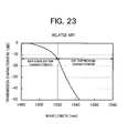
- the ASE light in the vicinity of 1530nm generated at this time is suppressed by the optical filter having a transmission wavelength characteristic as shown in Fig. 23.
- a gain deviation occurring at the time of amplification is flattened by the optical filter described above.
- the signal light having passed through the EDF and optical filters of each stage is output via a WDM coupler and an optical isolator at an output side to the optical transmission path.
- the present invention has been accomplished in view of the above problems, and it is an object of the present invention to provide an optical amplifier using an optical amplification medium doped with a rare earth element, for improving efficiency of optical amplification for a new wavelength band, such as S-band, that enables to realize the extension of a signal band of an optical transmission system, and also for enabling the realization of simplicity of constitution.
- one aspect of the present invention provides an optical amplifier using optical amplification mediums each doped with a rare earth element, for amplifying signal light in a predetermined wavelength band, wherein the optical amplifier has a center wavelength of a gain peak at an outside of a signal band, and a gain coefficient of when a pumping condition of said optical amplification medium is maximum is set so that an efficiency evaluation value obtained by dividing a minimum value of the gain coefficient in the signal band by a maximum value of the gain coefficient at the outside of the signal band becomes a previously set value or more.
- amplification efficiency of the signal light having the center wavelength of the gain peak at the outside of the signal band can be improved.
- the optical amplifier described above is preferably constituted so that the efficiency evaluation value is 0.15 or more.
- the wavelength band of the signal light may be constituted so that the center wavelength of the gain peak is located at the outside of the signal band on a longer wavelength side, and more specifically, the wavelength band of the signal light can be S-band of from 1480nm to 1530nm.
- the optical amplifier may comprise: a plurality of optical amplification mediums each doped with a rare earth element having a gain peak value for a wavelength; gain equalizers disposed between said optical amplification mediums, each equalizing a gain in a wavelength band in which the gain is tilted at a wavelength different from the wavelength having the peak value; and a temperature control section controlling a temperature of each of the optical amplification mediums to be a predetermined temperature.
- the efficiency evaluation value can be increased by the temperature control of the optical amplification medium.
- the optical amplifier may comprise: a plurality of optical amplification mediums each doped with a rare earth element having a gain peak value for a wavelength; and gain equalizers disposed between said optical amplification mediums, each equalizing a gain in a wavelength band in which the gain is tilted at a wavelength different from the wavelength having the peak value, wherein the optical amplification medium is doped with an additive that increases a gain coefficient of a wavelength in a band equalized by the gain equalizer.
- the efficiency evaluation value can be increased by using the optical amplification medium doped with the additive that increases the gain coefficient corresponding to the wavelength band equalized by the gain equalizer.
- the optical amplifier may comprise: a plurality of optical amplification mediums each doped with a rare earth element having a gain peak value for a wavelength; and gain equalizers disposed between said optical amplification mediums, each equalizing a gain in a wavelength band in which the gain is tilted at a wavelength different from the wavelength having the peak value, wherein for the optical amplification medium, a base material that increases a gain coefficient of a wavelength in a band equalized by the gain equalizer is used rather than a silica base material.
- the efficiency evaluation value can be increased in comparison with the optical amplification medium made of the silica base material.
- Fig. 1 is a diagram for explaining a basic concept of the present invention in which an example of a gain wavelength characteristic of a typical EDF is shown.
- the gain wavelength characteristic has a gain peak at the outside, on a longer wavelength side, of an S-band signal band corresponding to an area enclosed by oblique lines (more specifically, in the vicinity of 1530nm).
- a gain has a characteristic that is tilted with respect to the wavelength.
- a gain coefficient in S-band may be increased, or (B) the gain peak at the outside of the signal band may be reduced to suppress growth of ASE light in the vicinity of 1530nm.
- ⁇ g min / g peak
- g min a minimum gain coefficient at the inside of the signal band when a pumping state of the optical amplification medium is maximum
- g peak is a gain peak value (a maximum value of the gain coefficient) at the outside of the signal band.
- Fig. 2 shows an example of a relation of total output power of S-band signal light to ASE optical power in 1530nm band according to each value of a parameter ⁇ (0.18-0.21). It can be seen from Fig. 2 that the total output power of the S-band signal light is reduced drastically as the ASE light at the outside of the signal band grows. This is because pumping power to be supplied to the EDF is consumed by the growth of the ASE light. However, as the value of the parameter ⁇ is increased, the growth of the ASE light is suppressed and the pumping light power is mainly consumed by the amplification of the S-band signal light.
- Fig. 3 shows an example of a relation of amplification efficiency to the parameter ⁇ .
- the amplification efficiency is also increased as the parameter ⁇ is increased. More specifically, for example, in order to obtain the amplification efficiency of 6% or more, the parameter ⁇ may be set to 0.15 or more.
- the parameter ⁇ being a ratio between the gain peak value g peak at the outside of the signal band and the minimum value g min of the gain coefficient at the inside of the signal band is a very useful index in designing the optical amplifier that has the gain peak at the outside of the signal band.
- an EDF is assumed as the rare earth element doped optical fiber serving as the optical amplification medium, and S-band that is located at a shorter wavelength side of the peak wavelength is assumed as the wavelength band different from the peak wavelength.
- the present invention is not limited thereto, and it is possible to use an optical fiber doped with any rare earth element other than Erbium is used as the optical amplification medium, and to assume any wavelength band other than S-band in which the peak wavelength is located at the outside of the signal band.
- the optical amplifier according to the present invention constituted based on the design focusing on the parameter ⁇ as described above, the efficiency of the optical amplification for a new wavelength band such as S-band can be improved and the constitution can be simplified.
- a new wavelength band such as S-band
- Fig. 4 is a block diagram showing a constitutional example of an S-band EDFA according to a first embodiment of the present invention.
- the S-band EDFA comprises, for example, a plurality of silica based Erbium doped optical fiber (EDF) 3 that are cascade connected between an input port 1 and an output port 2, gain equalizers (GEQ) 4 inserted respectively at an output end of each EDF 3, pumping light sources 5 and WDM couplers 6 for supplying pumping light to each EDF 3, a temperature adjusting section 7 adjusting a temperature of each EDF 3, and optical isolators 8 inserted at a latter state of the input port 1 and at a previous stage of the output port 2, respectively.
- EDF Erbium doped optical fiber
- GEQ gain equalizers
- each EDF 3 A typical silica based EDF used for a conventional EDFA corresponding to C-band or L-band can be used as each EDF 3. It is assumed that the length of each EDF 3 is adjusted appropriately so that a required gain can be obtained in the present optical amplifier.
- Each GEQ 4 is a known optical filter having a transmission wavelength characteristic that can suppress ASE light outside S-band that is generated in each EDF 3, especially, ASE light generated in the vicinity of 1530nm, and at the same time, can compensate for a tilt of the gain coefficient in S-band. More specifically, for example, a Fabry-Perot etalon filter, a dielectric multi-layer film filter, or a fiber grating filter can be used. Note, it is assumed that each GEQ 4 can transmit the pumping light.
- Each pumping light sources 5 is a typical pumping light source that generates pumping light in a wavelength band, capable of pumping each EDF 3 (980nm band, 1480nm band and the like, for example).
- the pumping light output from the pumping light source 5 positioned at the input side is multiplexed at the WDM coupler 6 positioned at the input side in the same direction as a propagation direction of the signal light, to be supplied to each EDF 3.
- the pumping light output from the pumping light sources 5 positioned at the output side is multiplexed at the WDM couplers 6 positioned at the output side in an opposite direction to the propagation direction of the signal light, to be supplied to each EDF 3.
- the temperature adjusting section 7 that can adjust the temperature of each EDF 3 measures the temperature of each EDF 3 and adjusts the temperature of each EDF 3 to a predetermined temperature by temperature control means such as a heater provided in each EDF 3 or detects the parameter ⁇ based on the output of the optical amplifier and adjusts the temperature of each EDF, so as to realize the improvement of efficiency of the optical amplification for S-band.
- temperature control means such as a heater provided in each EDF 3 or detects the parameter ⁇ based on the output of the optical amplifier and adjusts the temperature of each EDF, so as to realize the improvement of efficiency of the optical amplification for S-band.
- Each optical isolator 8 is a known optical device transmitting light in only one direction.
- the optical isolator 8 disposed at the input side transmits the S-band signal light input to the input port 1 to the WDM coupler 6 at the input side and, at the same time, blocks transmission of light that is propagated in a direction opposite to the propagation direction of the signal light.
- the optical isolator 8 disposed at the output side transmits the light having passed through the WDM coupler 6 at the output side to the output port 2 and, at the same time, blocks transmission of light that is input from outside via the output port 2.
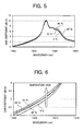
- Fig. 5 is a diagram showing a change in the gain coefficient of the EDF with respect to a change in temperature of 0°C, 20°C (room temperature), 40°C and 80°C, for example.
- Fig. 6 is an enlarged diagram of the characteristic shown in Fig. 5 for the S-band
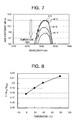
- Fig. 7 is an enlarged diagram of the characteristic in the vicinity of 1530nm shown in Fig. 5.
- Fig. 8 is a diagram showing a relation between the temperature of the EDF and the parameter ⁇ .
- the gain coefficient of the EDF has temperature dependence such that, as the temperature of the EDF rises, the gain coefficient in S-band is increased (Fig. 6) and the gain coefficient peak in the vicinity of 1530nm is lowered (Fig. 7). Therefore, as shown in Fig. 8, as the temperature of the EDF rises, the value of the parameter ⁇ is increased. Accordingly, by holding the EDF in a high temperature, it becomes possible to improve the amplification efficiency of the S-band EDFA.
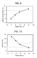
- Fig. 9 is a diagram showing temperature dependence of the amplification efficiency of this EDFA.
- Fig. 10 is a diagram showing temperature dependence of an average NF (noise figure) of this EDFA.
- each temperature dependence in Figs. 9 and 10 shows a characteristic of when each EDF 3 is constituted in five stages wherein the length of EDF per one stage is 4m and forward and backward pumping power is 240mW each, for the constitutional example shown in Fig. 4.
- optical signals of 40 channels are disposed with 100GHz spacing in the wavelength band of from 1489nm to 1519nm, and input light power to each channel is -15dBm/ch.
- the amplification efficiency is improved by about 1.5% and the average NF is improved by about 0.34dB.
- the amplification characteristic of the S-band EDFA described above is an example of when each EDF is constituted in the five stages, it has been confirmed that the values of the amplification efficiency and the average NF also depend on the number of stages of the EDF.
- Fig. 11 shows an example of dependence of the amplification efficiency on the number of stages
- Fig. 12 shows an example of dependence of the average NF on the number of stages. Note, each dependence on the number of stages in Figs. 11 and 12 shows a characteristic of when the number of stages is changed provided that the total length of the EDF is fixed to 20m and the output light power per one channel is fixed to OdBm/ch.
- the S-band signal light as in the above case, it is assumed that optical signals of 40 channels are disposed with 100GHz spacing in the wavelength band from 1489nm to 1519nm, and input light power to each channel is -15dBm/ch.
- the optimal constitution of S-band EDFA is changed depending on the temperature of the EDF 3, that is, the value of the parameter ⁇ . More specifically, by increasing the temperature of the EDF 3 to increase the parameter ⁇ , the number of stages of the EDF 3 can be reduced, and consequently, it becomes possible to simplify the constitution of the S-band EDFA.
- the parameter ⁇ is increased by increasing the temperature of the EDF.
- the direction of temperature change is not limited to the rising direction, but it should be determined according to the gain characteristic of the rare earth element doped optical fiber used as the optical amplification fiber and the setting of the signal band.
- the amplification efficiency is improved and the constitution is simplified, by increasing the temperature of the EDF by the temperature adjusting section 7 to increase the parameter ⁇ .
- the parameter ⁇ is increased by refining an additive in the EDF to be used as the optical amplification medium, in place of the temperature control of the EDF.
- Fig. 13 is a block diagram showing a constitutional example of an S-band EDFA according to the second embodiment of the present invention. Note, same components as in Fig. 4 above are denoted by same reference numerals and description thereof is omitted. Same rule will be applied to other embodiments.
- the second embodiment differs from the first embodiment in that a silica based EDF 3' doped with aluminum (Al) in high density is used as optical amplification medium at each stage in place of the temperature adjusting section 7.
- Al aluminum
- Each EDF 3' is the one in which a core of a typical silica based EDF is doped with Al 2 O 3 or the like. It is known that the gain wavelength characteristic of such an EDF 3' is changed according to the type or amount of additive.
- Fig. 14 is a diagram showing dependence of a relative gain coefficient on a doping amount of Al. As apparent from Fig. 14, as the doping amount of Al is increased, the relative gain coefficient for S-band tends to be increased.
- Table 1 shows the data when each EDF 3' is constituted in five stages wherein the length of the EDF per one stage is 4m, and forward and backward pumping power is 240mW each, for the constitutional example shown in Fig. 13.
- optical signals of 40 channels are disposed with 100GHz spacing in the wavelength band from 1489nm to 1519nm, and input light power to each channel is -15dBm/ch.
- the second embodiment by constituting the S-band EDFA using the EDF 3' doped with Al in higher density, it is possible to increase the parameter ⁇ to improve the amplification efficiency. Further, as in the first embodiment described above, since the amplification efficiency is improved to enable the reduction of the number of the EDF 3', it becomes possible to simplify the constitution of the S-band EDFA.
- the parameter ⁇ is increased by increasing the doping amount of Al.
- the additive for the EDF is not limited to Al, but any of various substances capable of changing the gain wavelength characteristic of the EDF so as to increase the parameter ⁇ can be used as the additive.
- Specific examples of the additives other than Al may include phosphorus, boron and the like.
- the parameter ⁇ is increased by using the silica based EDF in which the doping amount of Al is increased as the optical amplification medium.
- the parameter ⁇ is increased by refining a composition of base material (host glass) to be used as the optical amplification medium.
- Fig. 15 is a block diagram showing a constitutional example of an S-band EDFA according to the third embodiment of the present invention.
- the constitution of the third embodiment differs from the second embodiment in that, instead of the silica based EDF 3' doped with Al in high density, EDF 3" using either fluoride glass or tellurite glass as the host glass, for example, is used as the optical amplification medium at each stage.
- EDF 3 using either fluoride glass or tellurite glass as the host glass, for example, is used as the optical amplification medium at each stage.
- Components other than the above are the same as those of the second embodiment.
- Each EDF 3" is the one in which an optical fiber using the fluoride glass or the tellurite glass as the host glass is doped with erbium and the like. Generally, it is known that the gain wavelength characteristic of the EDF 3 is changed depending on the composition of the host glass.
- Fig. 16 is a diagram showing dependence of the relative gain coefficient on the host glass.
- the relative gain coefficient of each EDF in which each of three types of glasses, the silica glass (doped with Al in high density), the fluoride glass and the tellurite glass, is used as the host glass.
- the profile of the relative gain coefficient differs significantly depending on the type of the host glass, or in other words, the relative gain coefficient for S-band tends to be increased when the fluoride glass or the tellurite glass is used as the host glass.
- Table 2 data in which the parameters ⁇ for various types of the host glass are compared is shown in Table 2:
- the fluoride glass and the tellurite glass is suitable for the host glass.
- the amplification characteristic of the S-band EDFA according to this embodiment will be described specifically.
- the feature of this embodiment will be considered through the comparison of the case where the tellurite glass, for example, is used as the host glass for each EDF 3" and the case where the silica glass is used as the host glass, for the amplification characteristic of the S-band EDFA.
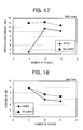
- Fig. 17 shows an example of dependence of the amplification efficiency on the number of stages
- Fig. 18 shows an example of dependence of the average NF on the number of the stages, in each of the S-band EDFAs using the tellurite glass and the silica glass, respectively.
- each dependence on the number of stages in Figs. 17 and 18 shows the characteristic of when the number of stages of EDF is changed provided that the total length of the EDF is fixed to 20m and the output light power per one channel is fixed to 0dBm/ch.
- optical signals of 40 channels are disposed with 100GHz spacing in the wavelength band from 1489nm to 1519nm, and input light power to each channel is -15dBm/ch. Therefore, the gain of the S-band EDFA is 15dB in this case.
- the amplification efficiency better than that in the S-band EDFA using the silica glass can be achieved, in particular, when each EDF is constituted in three stages, the amplification efficiency is improved by about 13% in comparison with the EDFA using the silica glass.
- the average NF is somewhat worse than that in the EDFA using the silica glass, but can obtain the characteristic that is substantially the same as that in the EDFA using the silica glass, by reducing the number of stages of the EDF to constitute three stages, for example.
- Figs. 19 and 20 show the dependence of the amplification efficiency on the number of stages and the dependence of the average NF on the number of stages, respectively, in the case where the input light power of each channel is set to -25dBm/ch to set the gain of the S-band EDFA to 25dB, for example.
- the amplification efficiency in the S-band EDFA using the silica glass as the host glass is significantly worse than the case where the gain is set to 15dB.
- the amplification efficiency in the S-band EDFA using the tellurite glass becomes worse when the EDF is constituted in three stages, but the better amplification efficiency can be achieved in the constitutions of four and five stages.
- a better average NF than that in the EDFA using the silica glass can be achieved.
- the S-band EDFA by constituting the S-band EDFA using the tellurite glass or the fluoride glass as the host glass of the EDF, it becomes possible to increase the parameter ⁇ to improve the amplification efficiency, and at the same time, to simplify the constitution of the S-band EDFA.
- the tellurite glass or the fluoride glass is used as the host glass of the EDF to increase the parameter ⁇ .
- the host glass of the EDF is not limited to the above examples, but it is possible to use, as the host glass, any of various materials that change the gain wavelength characteristic of the EDF so as to increase the parameter ⁇ .
- Specific examples of the host glass may include phosphate, borate and the like.
- the EDFA corresponding to S-band only has been described.
- a plurality of bands of signal light may be amplified collectively in one optical amplifier by combining the existing C-band EDFA, the L-band EDFA and the like. More specifically, it is possible to connect the existing EDFA for other band in parallel to the S-band EDFA according to the present invention, so that input signal light is branched for each band to perform the optical amplification in each EDFA.
Landscapes
- Physics & Mathematics (AREA)
- Electromagnetism (AREA)
- Engineering & Computer Science (AREA)
- Plasma & Fusion (AREA)
- Optics & Photonics (AREA)
- Computer Networks & Wireless Communication (AREA)
- Signal Processing (AREA)
- Lasers (AREA)
- Optical Fibers, Optical Fiber Cores, And Optical Fiber Bundles (AREA)
- Optical Communication System (AREA)
Abstract
Description


where the silica glass is used as the host glass, for the amplification characteristic of the S-band EDFA.
Claims (14)
- An optical amplifier comprising:a plurality of optical amplification mediums each doped with a rare earth element having a gain peak value for a wavelength;gain equalizers disposed between said optical amplification mediums, each equalizing a gain in a wavelength band in which the gain is tilted at a wavelength different from the wavelength having said peak value; anda temperature control section controlling a temperature of each of said optical amplification mediums to be a predetermined temperature.
- An optical amplifier comprising:wherein said optical amplification medium is doped with an additive that increases a gain coefficient of a wavelength in a band equalized by said gain equalizer.a plurality of optical amplification mediums each doped with a rare earth element having a gain peak value for a wavelength; andgain equalizers disposed between said optical amplification mediums, each equalizing a gain in a wavelength band in which the gain is tilted at a wavelength different from the wavelength having said peak value,
- An optical amplifier comprising:wherein for the optical amplification medium, a base material that increases a gain coefficient of a wavelength in a band equalized by said gain equalizer is used rather than a silica base material.a plurality of optical amplification mediums each doped with a rare earth element having a gain peak value for a wavelength; andgain equalizers disposed between said optical amplification mediums, each equalizing a gain in a wavelength band in which the gain is tilted at a wavelength different from the wavelength having said peak value,
- An optical amplifier using optical amplification mediums each doped with a rare earth element for amplifying signal light in a predetermined wavelength band,
wherein said optical amplifier has a center wavelength of a gain peak at an outside of a signal band, and a gain coefficient of when a pumping condition of said optical amplification medium is maximum is set so that an efficiency evaluation value obtained by dividing a minimum value of the gain coefficient in the signal band by a maximum value of the gain coefficient at the outside of the signal band becomes a previously set value or more. - An optical amplifier according to claim 4,
wherein said efficiency evaluation value is 0.15 or more. - An optical amplifier according to claim 4,
wherein the center wavelength of said gain peak is located at the outside of the signal band on a longer wavelength side. - An optical amplifier according to claim 6,
wherein said signal band is a wavelength band of from 1480nm to 1530nm. - An optical amplifier according to claim 4, further comprising;
a temperature adjusting section adjusting a temperature of each of said optical amplification mediums,
wherein said efficiency evaluation value is set to the previously set value or more based on the temperature adjusting by said temperature adjusting section. - An optical amplifier according to claim 8,
wherein when said optical amplification medium is an erbium doped optical fiber,
said temperature adjusting section increases the temperature of the erbium doped optical fiber to increase said efficiency evaluation value. - An optical amplifier according to claim 4,
wherein a medium doped with a predetermined additive in addition to the rare earth element is used for said optical amplification medium, and said efficiency evaluation value is set to the previously set value or more according to a doping amount of said additive. - An optical amplifier according to claim 10,
wherein when said optical amplification medium is an erbium doped optical fiber,
aluminum is used for said additive, and said doping amount is increased to said efficiency evaluation value. - An optical amplifier according to claim 4,
wherein for said optical amplification medium, a predetermined glass material is used as host glass, and said efficiency evaluation value is set to the previously set value or more according to a composition of said glass material. - An optical amplifier according to claim 12,
wherein when said optical amplification medium is an erbium doped optical fiber,
either fluoride glass or tellurite glass is sued as said host glass. - An optical amplifier according to claim 4, further comprising:said optical amplification medium disposed in plural numbers so as to be cascade connected to each other;a plurality of optical filter sections each connected to one end of each of said optical amplification mediums, and having a transmission characteristic capable of suppressing at least said gain peak at the outside of the signal band, that is generated in said optical amplification medium; anda pumping light supply section supplying pumping light to each of said optical amplification medium.
Priority Applications (1)
| Application Number | Priority Date | Filing Date | Title |
|---|---|---|---|
| EP06017397A EP1720271B1 (en) | 2002-06-24 | 2003-01-24 | Optical amplifier |
Applications Claiming Priority (2)
| Application Number | Priority Date | Filing Date | Title |
|---|---|---|---|
| JP2002182750 | 2002-06-24 | ||
| JP2002182750A JP4094352B2 (en) | 2002-06-24 | 2002-06-24 | Optical amplifier |
Related Child Applications (1)
| Application Number | Title | Priority Date | Filing Date |
|---|---|---|---|
| EP06017397A Division EP1720271B1 (en) | 2002-06-24 | 2003-01-24 | Optical amplifier |
Publications (3)
| Publication Number | Publication Date |
|---|---|
| EP1385279A2 true EP1385279A2 (en) | 2004-01-28 |
| EP1385279A3 EP1385279A3 (en) | 2005-06-15 |
| EP1385279B1 EP1385279B1 (en) | 2006-11-08 |
Family
ID=29728330
Family Applications (2)
| Application Number | Title | Priority Date | Filing Date |
|---|---|---|---|
| EP06017397A Expired - Lifetime EP1720271B1 (en) | 2002-06-24 | 2003-01-24 | Optical amplifier |
| EP03001355A Revoked EP1385279B1 (en) | 2002-06-24 | 2003-01-24 | Optical amplifier |
Family Applications Before (1)
| Application Number | Title | Priority Date | Filing Date |
|---|---|---|---|
| EP06017397A Expired - Lifetime EP1720271B1 (en) | 2002-06-24 | 2003-01-24 | Optical amplifier |
Country Status (4)
| Country | Link |
|---|---|
| US (1) | US8064130B2 (en) |
| EP (2) | EP1720271B1 (en) |
| JP (1) | JP4094352B2 (en) |
| DE (2) | DE60309543T2 (en) |
Families Citing this family (8)
| Publication number | Priority date | Publication date | Assignee | Title |
|---|---|---|---|---|
| JP5246725B2 (en) * | 2005-03-02 | 2013-07-24 | 住友電気工業株式会社 | Optical amplifier |
| JP2009076493A (en) * | 2007-09-18 | 2009-04-09 | Sumitomo Electric Ind Ltd | Amplifying optical fiber |
| JP5884654B2 (en) * | 2012-06-12 | 2016-03-15 | 富士通株式会社 | Optical amplifier and optical amplifier control method |
| PT2947728T (en) * | 2014-05-23 | 2018-05-02 | Padtec S A | Optical amplifier and related method |
| US10523334B1 (en) * | 2018-12-07 | 2019-12-31 | Fujitsu Limited | Controlling gain modulation in optical communication networks |
| CN112993738A (en) * | 2021-04-21 | 2021-06-18 | 武汉光迅科技股份有限公司 | S-band optical amplifier and implementation method thereof |
| CN115361066B (en) * | 2022-08-16 | 2023-09-26 | 北京邮电大学 | A gain equalization method and system for S-band signals |
| US20240079839A1 (en) * | 2022-09-01 | 2024-03-07 | Ii-Vi Delaware, Inc. | Temperature control for coiled gain fiber in fiber amplifier |
Family Cites Families (24)
| Publication number | Priority date | Publication date | Assignee | Title |
|---|---|---|---|---|
| JPH0411794A (en) | 1990-04-28 | 1992-01-16 | Furukawa Electric Co Ltd:The | Fiber type optical amplifier |
| US5337382A (en) * | 1992-05-29 | 1994-08-09 | At&T Bell Laboratories | Article comprising an optical waveguide with in-line refractive index grating |
| JP3422398B2 (en) * | 1995-12-07 | 2003-06-30 | 富士通株式会社 | Center-of-gravity wavelength monitoring method and apparatus, optical amplifier, and optical communication system |
| EP1433760B1 (en) * | 1997-02-14 | 2008-05-14 | Nippon Telegraph and Telephone Corporation | Optical fibre splicing structure |
| US5920424A (en) * | 1997-02-18 | 1999-07-06 | Lucent Technologies Inc. | Article comprising a broadband optical fiber amplifier |
| JP3597045B2 (en) | 1997-06-02 | 2004-12-02 | ルーセント テクノロジーズ インコーポレーテッド | Broadband optical amplifier, apparatus including the same, and method for amplifying optical signal |
| US6049417A (en) * | 1997-06-02 | 2000-04-11 | Lucent Technologies Inc. | Wide band optical amplifier |
| JP3452768B2 (en) * | 1997-08-11 | 2003-09-29 | 富士通株式会社 | Method and apparatus for optical amplification and system with the same |
| EP1055299A2 (en) * | 1998-02-20 | 2000-11-29 | SDL, Inc. | Upgradable, gain flattened fiber amplifiers for wdm applications |
| US6600592B2 (en) * | 1998-03-24 | 2003-07-29 | Xtera Communications, Inc. | S+ band nonlinear polarization amplifiers |
| JP3688131B2 (en) | 1998-09-10 | 2005-08-24 | 日本電信電話株式会社 | Optical amplification element |
| JP2000277842A (en) * | 1999-03-23 | 2000-10-06 | Oki Electric Ind Co Ltd | Optical components, and optical amplifier and characteristics control method for the same |
| US6344425B1 (en) * | 1999-11-19 | 2002-02-05 | Corning Incorporated | Fluorotellurite, amplifier glasses |
| JP2001313433A (en) | 2000-02-23 | 2001-11-09 | Fujitsu Ltd | Optical amplifier and optical amplification method |
| EP1128504B8 (en) * | 2000-02-23 | 2009-08-12 | Fujitsu Limited | Optical amplifier |
| JP2001252165A (en) | 2000-03-09 | 2001-09-18 | Yamato Kogyo Kk | Bamboo container for sake |
| US6519081B2 (en) * | 2000-04-13 | 2003-02-11 | Corning Incorporated | Method of operating a noise-compensating gain controller for an optical amplifier |
| EP1209779A1 (en) * | 2000-11-27 | 2002-05-29 | Alcatel | Optical fiber amplifier having a heating system for controlling the temperature of an amplifying fiber and corresponding method |
| JP2002171016A (en) * | 2000-11-30 | 2002-06-14 | Sumitomo Electric Ind Ltd | Optical filter, optical amplification system and optical communication system |
| US6529316B1 (en) * | 2001-05-03 | 2003-03-04 | Onetta, Inc. | Optical network equipment with optical channel monitor and dynamic spectral filter alarms |
| US6690506B2 (en) * | 2001-05-17 | 2004-02-10 | Corning Incorporated | Control architecture and method for optical amplifiers |
| US6621621B1 (en) * | 2001-06-07 | 2003-09-16 | Innovance, Inc. | Line amplification system for wavelength switched optical networks |
| DE60100599T2 (en) * | 2001-06-21 | 2004-04-08 | Alcatel | Optical device with multi-component oxide glass |
| JP2003069116A (en) * | 2001-08-22 | 2003-03-07 | Fujitsu Ltd | Optical amplifier and gain deviation compensation method |
-
2002
- 2002-06-24 JP JP2002182750A patent/JP4094352B2/en not_active Expired - Fee Related
-
2003
- 2003-01-24 DE DE60309543T patent/DE60309543T2/en not_active Expired - Lifetime
- 2003-01-24 DE DE60319891T patent/DE60319891T2/en not_active Expired - Lifetime
- 2003-01-24 EP EP06017397A patent/EP1720271B1/en not_active Expired - Lifetime
- 2003-01-24 EP EP03001355A patent/EP1385279B1/en not_active Revoked
- 2003-01-27 US US10/351,340 patent/US8064130B2/en not_active Expired - Fee Related
Also Published As
| Publication number | Publication date |
|---|---|
| EP1385279B1 (en) | 2006-11-08 |
| EP1720271A1 (en) | 2006-11-08 |
| DE60309543T2 (en) | 2007-08-30 |
| DE60319891D1 (en) | 2008-04-30 |
| EP1385279A3 (en) | 2005-06-15 |
| DE60319891T2 (en) | 2009-03-05 |
| US8064130B2 (en) | 2011-11-22 |
| US20030234976A1 (en) | 2003-12-25 |
| DE60309543D1 (en) | 2006-12-21 |
| JP2004031480A (en) | 2004-01-29 |
| JP4094352B2 (en) | 2008-06-04 |
| EP1720271B1 (en) | 2008-03-19 |
Similar Documents
| Publication | Publication Date | Title |
|---|---|---|
| JP4900501B2 (en) | Optical amplifier and optical amplification method | |
| CN1917307B (en) | Optical amplifier for amplifying multi-wavelength light | |
| JPH04233519A (en) | Multistage optical fiber amplifier | |
| CA2346664A1 (en) | Management and utilization of ase in optical amplifier | |
| US7072100B2 (en) | Optical amplifier and gain tilt compensation method | |
| Sakamoto et al. | Hybrid fiber amplifiers consisting of cascaded TDFA and EDFA for WDM signals | |
| JP2001313433A (en) | Optical amplifier and optical amplification method | |
| EP1720271B1 (en) | Optical amplifier | |
| US7773295B2 (en) | Optical amplication module, optical amplifier, optical communication system, and white light source | |
| JP5103963B2 (en) | Multistage optical amplifier and control method thereof | |
| EP1220385B1 (en) | Optical amplifier and method for amplifying wavelength multiplexed transmission signal light | |
| JP4145684B2 (en) | Optical amplification module, optical amplifier, optical communication system, and white light source | |
| JP3811134B2 (en) | Optical amplifier | |
| JPH09138432A (en) | Optical amplifier | |
| JP2003258348A (en) | Optical amplifier and optical communication system | |
| JP2019216240A (en) | Complementary optical fiber-based amplifiers with built-in gain flattening | |
| JP4100101B2 (en) | Optical amplifier and optical transmission system using the same | |
| JP4568247B2 (en) | Optical amplification module and optical amplifier including the same | |
| JP2003188445A (en) | Optical amplifier and optical amplification parts | |
| EP1355392B1 (en) | Optical amplification module | |
| Nilsson et al. | Alternating cascade of spectrally different erbium-doped fiber amplifiers for link-loss-insensitive long-haul WDM transmission | |
| Kakui et al. | Low noise, high power optical amplifiers employing an improved hybrid Er-doped fiber configuration for WDM transmission |
Legal Events
| Date | Code | Title | Description |
|---|---|---|---|
| PUAI | Public reference made under article 153(3) epc to a published international application that has entered the european phase |
Free format text: ORIGINAL CODE: 0009012 |
|
| AK | Designated contracting states |
Kind code of ref document: A2 Designated state(s): AT BE BG CH CY CZ DE DK EE ES FI FR GB GR HU IE IT LI LU MC NL PT SE SI SK TR |
|
| AX | Request for extension of the european patent |
Extension state: AL LT LV MK RO |
|
| PUAL | Search report despatched |
Free format text: ORIGINAL CODE: 0009013 |
|
| AK | Designated contracting states |
Kind code of ref document: A3 Designated state(s): AT BE BG CH CY CZ DE DK EE ES FI FR GB GR HU IE IT LI LU MC NL PT SE SI SK TR |
|
| AX | Request for extension of the european patent |
Extension state: AL LT LV MK RO |
|
| 17P | Request for examination filed |
Effective date: 20050921 |
|
| AKX | Designation fees paid |
Designated state(s): DE FR GB |
|
| GRAP | Despatch of communication of intention to grant a patent |
Free format text: ORIGINAL CODE: EPIDOSNIGR1 |
|
| GRAS | Grant fee paid |
Free format text: ORIGINAL CODE: EPIDOSNIGR3 |
|
| GRAA | (expected) grant |
Free format text: ORIGINAL CODE: 0009210 |
|
| AK | Designated contracting states |
Kind code of ref document: B1 Designated state(s): DE FR GB |
|
| REG | Reference to a national code |
Ref country code: GB Ref legal event code: FG4D |
|
| REF | Corresponds to: |
Ref document number: 60309543 Country of ref document: DE Date of ref document: 20061221 Kind code of ref document: P |
|
| ET | Fr: translation filed | ||
| PLBI | Opposition filed |
Free format text: ORIGINAL CODE: 0009260 |
|
| 26 | Opposition filed |
Opponent name: NOKIA SIEMENS NETWORKS OY Effective date: 20070808 |
|
| PLBD | Termination of opposition procedure: decision despatched |
Free format text: ORIGINAL CODE: EPIDOSNOPC1 |
|
| PLAU | Termination of opposition procedure: information related to despatch of decision deleted |
Free format text: ORIGINAL CODE: EPIDOSDOPC1 |
|
| PLAX | Notice of opposition and request to file observation + time limit sent |
Free format text: ORIGINAL CODE: EPIDOSNOBS2 |
|
| PLAF | Information modified related to communication of a notice of opposition and request to file observations + time limit |
Free format text: ORIGINAL CODE: EPIDOSCOBS2 |
|
| PLBB | Reply of patent proprietor to notice(s) of opposition received |
Free format text: ORIGINAL CODE: EPIDOSNOBS3 |
|
| RDAF | Communication despatched that patent is revoked |
Free format text: ORIGINAL CODE: EPIDOSNREV1 |
|
| APBM | Appeal reference recorded |
Free format text: ORIGINAL CODE: EPIDOSNREFNO |
|
| APBP | Date of receipt of notice of appeal recorded |
Free format text: ORIGINAL CODE: EPIDOSNNOA2O |
|
| APAH | Appeal reference modified |
Free format text: ORIGINAL CODE: EPIDOSCREFNO |
|
| APBQ | Date of receipt of statement of grounds of appeal recorded |
Free format text: ORIGINAL CODE: EPIDOSNNOA3O |
|
| PLAB | Opposition data, opponent's data or that of the opponent's representative modified |
Free format text: ORIGINAL CODE: 0009299OPPO |
|
| R26 | Opposition filed (corrected) |
Opponent name: NOKIA SIEMENS NETWORKS OY Effective date: 20070808 |
|
| PLAB | Opposition data, opponent's data or that of the opponent's representative modified |
Free format text: ORIGINAL CODE: 0009299OPPO |
|
| APBU | Appeal procedure closed |
Free format text: ORIGINAL CODE: EPIDOSNNOA9O |
|
| R26 | Opposition filed (corrected) |
Opponent name: NOKIA SOLUTIONS AND NETWORKS OY Effective date: 20070808 |
|
| REG | Reference to a national code |
Ref country code: FR Ref legal event code: PLFP Year of fee payment: 13 |
|
| PLAB | Opposition data, opponent's data or that of the opponent's representative modified |
Free format text: ORIGINAL CODE: 0009299OPPO |
|
| R26 | Opposition filed (corrected) |
Opponent name: NOKIA SOLUTIONS AND NETWORKS OY Effective date: 20070808 |
|
| REG | Reference to a national code |
Ref country code: FR Ref legal event code: PLFP Year of fee payment: 14 |
|
| RIC2 | Information provided on ipc code assigned after grant |
Ipc: H04B 10/29 20130101AFI20160713BHEP Ipc: H01S 3/00 20060101ALI20160713BHEP |
|
| REG | Reference to a national code |
Ref country code: FR Ref legal event code: PLFP Year of fee payment: 15 |
|
| PGFP | Annual fee paid to national office [announced via postgrant information from national office to epo] |
Ref country code: FR Payment date: 20161215 Year of fee payment: 15 |
|
| PGFP | Annual fee paid to national office [announced via postgrant information from national office to epo] |
Ref country code: DE Payment date: 20170117 Year of fee payment: 15 |
|
| PGFP | Annual fee paid to national office [announced via postgrant information from national office to epo] |
Ref country code: GB Payment date: 20170118 Year of fee payment: 15 |
|
| RDAD | Information modified related to despatch of communication that patent is revoked |
Free format text: ORIGINAL CODE: EPIDOSCREV1 |
|
| REG | Reference to a national code |
Ref country code: DE Ref legal event code: R064 Ref document number: 60309543 Country of ref document: DE Ref country code: DE Ref legal event code: R103 Ref document number: 60309543 Country of ref document: DE |
|
| RDAG | Patent revoked |
Free format text: ORIGINAL CODE: 0009271 |
|
| STAA | Information on the status of an ep patent application or granted ep patent |
Free format text: STATUS: PATENT REVOKED |
|
| 27W | Patent revoked |
Effective date: 20171002 |
|
| GBPR | Gb: patent revoked under art. 102 of the ep convention designating the uk as contracting state |
Effective date: 20171002 |