EP1383172A2 - Organic electroluminescent display device - Google Patents
Organic electroluminescent display device Download PDFInfo
- Publication number
- EP1383172A2 EP1383172A2 EP03016176A EP03016176A EP1383172A2 EP 1383172 A2 EP1383172 A2 EP 1383172A2 EP 03016176 A EP03016176 A EP 03016176A EP 03016176 A EP03016176 A EP 03016176A EP 1383172 A2 EP1383172 A2 EP 1383172A2
- Authority
- EP
- European Patent Office
- Prior art keywords
- light
- organic electroluminescent
- display device
- color
- electroluminescent display
- Prior art date
- Legal status (The legal status is an assumption and is not a legal conclusion. Google has not performed a legal analysis and makes no representation as to the accuracy of the status listed.)
- Withdrawn
Links
Images




Classifications
-
- H—ELECTRICITY
- H10—SEMICONDUCTOR DEVICES; ELECTRIC SOLID-STATE DEVICES NOT OTHERWISE PROVIDED FOR
- H10K—ORGANIC ELECTRIC SOLID-STATE DEVICES
- H10K59/00—Integrated devices, or assemblies of multiple devices, comprising at least one organic light-emitting element covered by group H10K50/00
- H10K59/30—Devices specially adapted for multicolour light emission
-
- H—ELECTRICITY
- H05—ELECTRIC TECHNIQUES NOT OTHERWISE PROVIDED FOR
- H05B—ELECTRIC HEATING; ELECTRIC LIGHT SOURCES NOT OTHERWISE PROVIDED FOR; CIRCUIT ARRANGEMENTS FOR ELECTRIC LIGHT SOURCES, IN GENERAL
- H05B33/00—Electroluminescent light sources
- H05B33/12—Light sources with substantially two-dimensional [2D] radiating surfaces
- H05B33/14—Light sources with substantially two-dimensional [2D] radiating surfaces characterised by the chemical or physical composition or the arrangement of the electroluminescent material, or by the simultaneous addition of the electroluminescent material in or onto the light source
-
- H—ELECTRICITY
- H10—SEMICONDUCTOR DEVICES; ELECTRIC SOLID-STATE DEVICES NOT OTHERWISE PROVIDED FOR
- H10K—ORGANIC ELECTRIC SOLID-STATE DEVICES
- H10K59/00—Integrated devices, or assemblies of multiple devices, comprising at least one organic light-emitting element covered by group H10K50/00
- H10K59/30—Devices specially adapted for multicolour light emission
- H10K59/38—Devices specially adapted for multicolour light emission comprising colour filters or colour changing media [CCM]
Definitions
- the present invention relates to an organic electroluminescent display device including light-emitting films containing organic electroluminescent materials.
- the electroluminescence (hereafter, referred to as EL) of organic compound materials which emit light by current injection is utilized in display devices (organic EL display devices).
- the EL display device has many pixels arrayed in a predetermined pattern on a planar substrate. Each pixel is composed of organic EL display elements made of organic EL films.
- organic compound materials which can emit red (R), green (G) and blue (B) light of high purity have been developed, which are suited for organic luminescent displays represented by the organic EL display device.
- R red
- G green
- B blue
- full color display devices which have R, G and B light-emitting elements in each pixel.
- Fig. 1 is a diagram illustrating a prior art organic electroluminescent display device, which is capable of providing color images, as disclosed in Japanese Patent Application Laid-open No. Hei 8-227276.
- this organic electroluminescent display device On a transparent substrate 1, this organic electroluminescent display device has scan signal lines 2 and data signal lines 3 which are arrayed to intersect at right angles and electrically isolated from each other, non-linear elements 4 each connected to the scan signal line 2 and the data signal line 3, and first display electrodes 5, which are connected to the non-linear elements 4, of independent array patterns each corresponding to the R, G and B light-emitting elements.
- first display electrode 5 On the first display electrode 5, a different organic electroluminescent film is deposited for each color, and a common second display electrode (not shown) is further deposited on the organic electroluminescent film.
- R, G and B light-emitting elements constitute a display unit (pixel) in combination, and full-color images are provided by driving the individual light-emitting elements.
- Japanese Patent Application Laid-open No. Hei.11-52905 discloses a technique using two light-emitting diodes (LEDs) of different colors per pixel for providing multicolor images by mixing the two gray-scaled colors.
- the present invention focuses on concentrations of organic electroluminescent materials, device structure and selected materials, so as to control the chromaticity of emitted light and thereby solve the above problems.
- An object of the present invention is to provide an organic electroluminescent display device that presents high-quality color images by mixing two colors emitted from selected two light-emitting elements of which chromaticity values are properly controlled.
- the aperture ratio becomes high and the manufacturing process becomes simple, while high-quality color images are provided.
- the two-color structure can save the use of organic materials, compared with the three-color structure.
- the present invention provides characteristics as follows.
- an organic electroluminescent display device including a plurality of light-emitting elements which are formed above a substrate by light-emitting films each containing organic electroluminescent materials and being sandwiched by a pair of electrodes, wherein each pixel of the display device is formed by two light-emitting elements producing two different colors of predetermined chromaticity values and each of the color has a gradation.
- the present invention utilizes an advantage of organic electroluminescent elements that the chromaticity of emitted light can be changed as desired to some extent.
- Fig. 2 is a CIE xy chromaticity diagram illustrating an embodiment of the present invention
- the colors produced by the R, G, and B light-emitting elements are set to have chromaticity values (L R , L G , L B ) of high purity
- the chromaticity gamut becomes large and versatile color imaging are provided with the three-color structure.
- one tries to produce color images from only two of R, G and B i.e.
- chromaticity values of E R , E G and E B produced by organic electroluminescent elements are not so pure as L R , L G and L B .
- the chromaticity values of E R , E G and E B can be shifted toward G or B side, R or B side, and G or R side under various setting conditions, respectively. Then, if two colors, for example, (E R1 , E B1 ) are selected, their combination can produce colors close to pure white O in the chromaticity diagram. By controlling the gradation of each color, the two colors can be shifted toward the E R side and E B side, with a near-white color in the center. Then versatile high-quality quasi-color images are provided.
- a second characteristic of the present invention is based on the above-mentioned first characteristic, in which a mixture of the two different colors can produce a white color which is designated by a white region in a CIE xy chromaticity diagram.
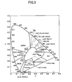
- the chromaticity values of the two selected colors are controlled so that the coordinate of combination (E R , E G ), (E G , E B ) or (E R , E B ) with respect to the chromaticity values of E R , E G and E B falls within a circular range Sw as the white color region in the CIE xy chromaticity diagram of JIS Z 8110, as shown in Fig. 3. Then the chromaticity coordinates can be moved toward the E R , E G or E B side with the white color disposed in the center, and versatile high-quality quasi-color images can be provided.
- a third characteristic is based on the display device described in the first characteristic, in which a mixture of the two different colors can produce color whose choromaticity falls within a circular area of a 0.1 radius with its center in the coordinate (0.31,0.316) of the pure white O in the CIE xy chromaticity diagram.
- the versatile high-quality quasi-color images can be produced because the chromaticity of color mixture can be moved from that of a near-white color toward that of E R , E G or E B to shift colors.
- a forth characteristic is based on the foregoing characteristics, in which the two different colors are selected from red (R), green (G), blue (B), cyan (C), magenta (M) and yellow (Y).
- the above color combinations (E R , E G ), (E G , E B ) and (E R , E B ), for example, may be (R, G), (G, B) and (R, B). If E R is shifted toward the G side, it turns to be yellow (Y). Then it produces another combination (Y, B) . In this way, the chromaticity coordinates of color mixture can be moved to the E R , E G or E B side, with a near-white color in the center, and so high-quality quasi-color images can be provided.
- a fifth characteristic is that one of the two different colors is white and the other is one selected from red (R), green (G), blue (B), cyan (C), magenta (M) and yellow (Y). Then the produced color can be changed from white to other colors, and thereby versatile high-quality quasi-color images are provided.
- a sixth characteristic is based on the foregoing characteristics, in which the chromaticity value is controlled by changing the concentration of the organic electroluminescent materials or by coupling with foreign materials.
- a seventh characteristic is based on the foregoing characteristics, in which the chromaticity value is controlled by varying the thickness of the electroluminescent film.
- Some organic electroluminescent elements have a layered structure composed of various functional films, such as a hole injection layer, a hole transport layer, a light emitting layer, an electron transport layer and an electron injection layer, for providing electroluminescent films.
- a hole injection layer such as a hole injection layer, a hole transport layer, a light emitting layer, an electron transport layer and an electron injection layer
- electroluminescent films such as a hole injection layer, a hole transport layer, a light emitting layer, an electron transport layer and an electron injection layer, for providing electroluminescent films.
- An eighth characteristic is based on the foregoing characteristics, in which each of the two light-emitting elements described above is formed by photo bleaching to the light-emitting films.
- This photo bleaching process produces two light-emitting elements with different colors from the light-emitting film formed uniformly. That is, light-emitting films, which form two light-emitting elements composing a pixel, may be produced with the same structure or material.
- the photo bleaching process radiates electromagnetic wave (or light) partially to an organic light-emitting film, including organic dye working as luminescent centers, to degrade the organic dye at the exposed part by photoxidation or photodecomposition. Then, using this effect that the exposed and non-exposed part has different colors respectively, this process can produce two different color light-emitting elements.
- the film may contain a plurality of kinds of organic dyes; in this case one or more kinds of dyes will be degraded.
- Electromagnetic wave used has wavelength in the range from 10 -17 to 10 5 m, involving ⁇ -ray, X-ray, ultraviolet-ray, visible light, infrared. Ultra-violet and visible lights are usually used.
- the formation of two different color light-emitting elements by the photo-bleaching process makes it possible to provide versatile high-quality quasi-color images by setting the chromaticity of the two color of emitting lights to that of near white.
- the fabrication in this process is easier, comparing with an individual patterning process which forms each light-emitting element from each pattern since there is no necessity of the individual pattering.
- the chromaticity control in this case can be conducted by varying the intensity of irradiation, exposure time, or by changing a species of organic dyes in the light-emitting film, or the combination of these.
- a ninth characteristic is based on the foregoing characteristic, in which the light-emitting elements are respective formed of color conversion filters that convert the light color from the light-emitting film.
- This color conversion filter method produces two light-emitting elements with different colors from the light-emitting film formed uniformly. That is, light-emitting films, which form two light-emitting elements composing a pixel, may be produced with the same structure or material.
- the color conversion filter method is classified into two categories; color filter method and fluorescent color conversion method. Even the formation of two colors by these methods also makes it possible to provide versatile high-quality quasi-color images by appropriately setting the chromaticity of the two colors with the near-white color in the center.
- the fabrication by this method is also easier, comparing with the individual patterning process since there is no necessity of the individual patterning.
- a tenth characteristic is that color conversion filters are used as the color filter method.
- the color filters may be formed by any one of the well-known fabrication methods as follows:
- Dyeing method is a method for forming each filter pattern from photosensitive dye substance, which is made from gelatin, glue or polyvinyl alcohol by applying dichromic acid processing.
- Pigment diffusion methods include methods for forming each color filter pattern from colored resins, which are made from such resin as polyimido with diffusion of pigments, and methods for forming filter patterns from colored resins, which are made from such negative-resist as acrylic epoxy series or cross-linked type polyvinyl alcohol with diffusion of pigments.
- Electrodeposition methods are patterning methods using electrochemical deposition in electrolytic solvent, dissolving such anionic resins as polyester resin or melanin resin, in which pigments diffuse.
- Printing methods are methods for forming each color filter by printing inks, which are made from pigments, oleic acid or stearic acid, phenol alcohol and additives (for drying or adjusting viscosity).
- An eleventh characteristic is using a fluorescent color conversion filter as a color conversion method.
- the filters absorb the near-ultraviolet or blue and blue-green lights from organic light-emitting film, and emit visible lights such as blue or blue-green to red by fluorescent emission.
- Fluorescent materials are, for example, shown below, but not limited to these.
- the above-mentioned fluorescent materials converting near-ultraviolet lights into blue lights include Bis-MSB(1,4-Bis(2-methylstyryl)benzene), DPS(trans-4,4-diphenylstylbenzene), coumarin4(7-hydroxy-4-methylcoumarin).
- Fluorescent materials converting blue lights into green lights include coumarinl53(2,3,5,6-1H,4H-tetrahydro-8-trifluromethylquinolizino(9,9a,1-gh) coumarin), coumarin6(3-(2'-benzothiazolyl)-7-diethylaminocoumarin), coumarin7(3-(2'-benzimidazolyl)-7-N,N-diethylaminocoumarin).
- Fluorescent materials converting blue-green lights into red lights include DCM(4-dicyanomethylene-2-methyl-6-(p-dimethylaminostyryl)-4H-pyrane), pyridinel(1-ethyl-2-(4-(p-dimethylaminophenyl)-1,3-butadienyl)-pyridinium-perchlorate), and rhodamin dyes.
- the above mentioned fluorescent materials and resins or photo resists (being preferable to be transparent) containing fluorescent materials are deposited on a transparent substrate by the process of vapor deposition, spattering or optical lithography being described in the formation of the color filter, to produce color conversion filters.
- color conversion filter can be formed on color filter. If the color of the color conversion filter is adjusted to that of the underneath color filter, the problem that color conversion filters are fluorescent by the excitation of environmental lights to decrease the display contrast, can be eliminated.
- a twelfth characteristic is based on the foregoing characteristics, in which the light-emitting film is produced by coating or printing process.
- the light-emitting films are fluorescent polymer layers formed by coating or printing process.
- the polymer layer may be formed as single layer of fluorescent polymer or multi-layers containing a hole transport layer, a fluorescent emitting polymer layer and the like.
- the fluorescent polymer layers can be formed from solutions, which dissolve low molecular weight fluorescent dyes such as coumarin, perylene, pyrane, anthron, porphyrin, quinacridon, N,N'-dialkyl-substituted quinacridon or naphthalimido, N,N'-diaryl-substituted pyrrolopyrrole in polymers such as polystyrene, polymethyl methacrylate, polyvinyl carbazole.
- the fluorescent polymer layers can also be formed from solutions of fluorescent polymers such as polyaryl vinylene, polyfluorene, the solvents of which involve toluene, xylene, acetone, methyl ethyl ketone, methyl isobutyl ketone, cyclohexanone, methanol, ethanol, isopropyl alcohol, ethyl acetate, butyl acetate, water or a mixture of these.
- the formation of these uniform or patterning layers of fluorescent polymers can be conducted by coating or printing process including spin coating, spray coating, flexography, gravure printing, micro-gravure printing, and intaglio offset lithography.
- a thirteenth characteristic is based on the foregoing characteristics, in which each emissive area of the two light-emitting elements with different colors is determined by taking each lifetime into consideration, to have nearly equal lifetimes.
- a fourteenth characteristic is based on the foregoing characteristic, in which the light-emitting element is driven by an electric current of a different level for each color.
- a fifteenth characteristic is based on the foregoing characteristic, in which that the light-emitting element is driven by a voltage of a different level for each color.
- the aperture ratio per pixel is higher than that of the RGB three-color system.
- the two-color system is easy to manufacture, compared with the three-color system.
- the following two light-emitting elements forming a pixel have the respective different structure or material of light-emitting film.
- the light-emitting elements are formed by the photo bleaching process or the color conversion filter (color filter or fluorescent color conversion filter) process, the light emitting film for the two light-emitting elements may be formed with the same structure and material.
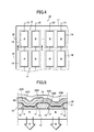
- Figs. 4 and 5 are diagrams illustrating the organic electroluminescent display device of one embodiment of the present invention
- Fig. 4 a schematic plan view illustrating part of the organic electroluminescent display device
- Fig. 5 a sectional view (taken along the line X-X in Fig. 4) of a vicinity of a pixel of the organic electroluminescent display device.
- the organic electroluminescent display device 10 has scan signal lines 12 and data signal lines 13 which intersect each other at right angles on a substrate 11, electrically isolated from each other, and first display electrodes 14 of independent array patterns each corresponding to the light-emitting elements R and B.
- Each of the first display electrodes 14 is connected to the scan signal line 12 and data signal line 13 (directly connected, or indirectly connected via a non-linear element (not shown) such as thin film transistor).
- a non-linear element such as thin film transistor
- all the data signal lines 13 are drawn to one side of the substrate 11 in this embodiment, those for the light-emitting elements R and B may be separated and drawn to either side each.
- one pixel P is composed of two (R: red; and B: blue) light-emitting elements.
- Multicolor images are provided by controlling the gradation of each of the light-emitting elements R and B independently (by passive matrix drive scheme or active matrix drive scheme).
- the substrate 11 is a transparent substrate made of, for example, glass
- the first display electrode 14 is a transparent electrode made of a transparent conductive material such as ITO (indium tin oxide).
- a dielectric film 15 made of, for example, polyimide, is formed to fill in between the first display electrodes 14, where signal lines are provided.
- the second display electrode 16 is a metallic electrode made of, for example, aluminum.
- a hole injection layer 21 and a hole transport layer 22 are formed on the first display electrode 14 and dielectric film 15 on the substrate 11.
- a first light-emitting layer 23R, an electron transport layer 24R and an electron injection layer 25R are formed one onto another over the selected area corresponding to the first display electrode 14 to produce a first color.
- a second light-emitting layer 23B, an electron transport layer 24B and an electron injection layer 25B are formed one onto another to produce a second color.
- the second display electrode 16 is deposited. In this way, the respective light-emitting elements R and B are formed over the areas corresponding to the second display electrode 16 and the first display electrode 14 which intersect each other.
- the CIE chromaticity of each emitted color can be set to a desired value by selecting dopant materials or their concentrations in the light-emitting layers 23R and 23B.
- dopant materials or their concentrations in the light-emitting layers 23R and 23B For example, if DCM (Di Cyano Methylene) is used as a dopant in the host material of Alq 3 in the light-emitting layer 23R corresponding to the R (red) light-emitting element, the CIE chromaticity, E R2 (0.52, 0.43), is obtained in the chromaticity diagram of Fig. 2.
- the chromaticity can be changed by varying the dopant concentration in the range of 0.1 to a few percent.
- two kinds of dopants can be used in combination in the host material of Alq 3 in the R (red) light-emitting layer 23R corresponding to the R light-emitting element.
- One of such dopant pairs is a combination of rubrene and DCM2 (Di Cyano Methylene2).
- DCM2 Di Cyano Methylene2
- perylene in the light-emitting layer 23B corresponding to the B (blue) light-emitting element, perylene can be used as a dopant in the host material of Alq 3 to produce a CIE chromaticity E B2 (0.14, 0.15) in Fig. 2.
- a white color of chromaticity (0.31, 0.34) can be provided by a two-color layered structure where the aforementioned yellow light-emitting layer is deposited on the blue light-emitting layer 23B in the B light-emitting element.
- this white light-emitting element By combining this white light-emitting element with the aforementioned R light-emitting element or with one of among green (G), blue (B), cyan (C), magenta (M) and yellow (Y), the color can be changed from white to a single color.
- the above organic electroluminescent display device 10 it is possible to change chromaticity of emitted light by changing the hole injection layer 21 and the hole transport layer 22 (hole transport functional layer) in thickness, while using the same materials for the electroluminescent film 20,
- the mechanism behind this is reflection/interference between the layers as described before. Indeed, the CIE chromaticity of R and that of B can be shifted toward the G side in the individual light-emitting elements R and B, while the CIE chromaticity of G can be shifted toward the R side in the G light-emitting element.
- various colors can be produced in the circular area, S o , of a radius of 0.1, with pure white O (0.31, 0.316) in its center, as shown in Fig. 2.
- the light-emitting elements R and B (corresponding to the position of the first display electrode 14) in the organic electroluminescent display device 10 that shows images with dots are arrayed in a grid pattern as shown in Fig. 4. Different colors may be arrayed at least every other line in the figure, but the array pattern is not limited to this grid one.
- Fig. 6(a) is a pattern where the light-emitting elements R and B are arrayed in a grid pattern and the color is alternated at least every other row.
- Fig. 6(b) is a similar pattern, but the first display electrodes 14 are extended in the lateral direction.
- the scan signal lines 12 are drawn to the left side of the substrate 11, and the data signal lines 13 are drawn to the top side.
- the data signal lines 13 may be separated by color and drawn to either top or bottom side each. Further, in a similar pattern, different colors may be arrayed every other row and column.
- the light-emitting elements R and B are arrayed in a staggered pattern and the color is changed at least every other row.
- the scan signal lines 12 are drawn to the left side of the substrate 11 and the data signal lines 13 are drawn to the top side.
- the data signal lines 13 may be separated by color and drawn to either top or bottom side each. Further, in a similar pattern, different colors may be arrayed every other column.
- the light-emitting elements R and B are arrayed in a staggered pattern, and the color is changed at least every other row and column.
- the scan signal lines 12 are drawn to the left side of the substrate 11, and the data signal lines 13 are separated by color and drawn to either top or bottom side each.
- the organic electroluminescent elements forming the light-emitting elements R and B are driven by an electric current or voltage. Each color is driven by the respective different current or voltage. Then by controlling the gradation of each color independently, even a two-color structure can provide various colors, with white in the center, for achieving high-quality quasi-color imaging.
- the chromaticity controlled by the above table is E R1 (0.61, 0.39) and E B1 (0.17, 0.30) respectively, and shown in CIE xy chromaticity diagram in Fig. 7.
- Colors on the line segment between E R1 and E B1 in Fig. 7 can be displayed on this display device, by controlling each gradation of the two light-emitting elements.
- the point on this line segment nearest to the pure white (0.31, 0.316) is an objective white, the chromaticity of which is Eo(0.31, 0.33).
- each required brightness of light-emitting element R and B is 18cd/m 2 and 32cd/m 2 , respectively.
- the measured lifetimes of light-emitting elements at the brightness ratio mentioned above allow us to design a ratio of emissive areas of light-emitting elements, to equalize the different lifetimes.
- the measured value in lifetime of light-emitting element R and B is 5000 hours and 2500 hours, respectively, in the case of a passive matrix panel with 50% aperture ratio and 1/64 duty drive.
- the lifetime is measured as a decreasing ratio of brightness vs. time at normal temperature.
- the design of area ratio with regard to this lifetime is shown in the following Table 2.
- the light-emitting elements R and B have been exemplified.
- any combination among R and G, G and B, or any two colors among red (R), green (G), blue (B), cyan (C), magenta (M) and yellow (Y) may be used in the two-color structure.
- the combinations of white and one of the above six colors may be used.
Landscapes
- Electroluminescent Light Sources (AREA)
- Devices For Indicating Variable Information By Combining Individual Elements (AREA)
Abstract
Description
| AN EXAMPLE FOR CHROMATICITY SETTING OF LIGHT-EMITTING ELEMENT R AND B | ||
| CONSTITUTION OF LIGHT-EMITTING ELEMENT R | CONSTITUTION OF LIGHT-EMITTING ELEMENT B | |
| HOLE INJECTION LAYER | CuPc | CuPc |
| (FILM THICKNESS) | 20nm | 20nm |
| HOLE TRANSPORT LAYER | α-NPD | α-NPD |
| (FILM THICKNESS) | 40nm | 40nm |
| LIGHT-EMITTING LAYER | ||
| HOST | Alq3 | IDE120 |
| GUEST | DCJTB | IDE102 |
| (FILM THICKNESS) | 30nm | 30nm |
| ELECTRON TRANSPORT LAYER | Alq3 | Alq3 |
| (FILM THICKNESS) | 50nm | 20nm |
| CATHODE | Mg-Ag | Mg-Ag |
| (FILM THICKNESS) | 100nm | 100nm |
| CHROMATICITY | (0.61, 0.39) | (0.17, 0.30) |
| AN EXAMPLE FOR AREA RATIO DESIGN WITH REGARD TO LIFETIME OF ELEMENT | ||||
| CHROMATICITY (x,y) | BRIGHTNESS | LIFETIME | AREA RATIO | |
| ELEMENT B | (0.17, 0.30) | 32 cd/m2 | 2500 hrs. | 2 |
| ELEMENT R | (0.61, 0.39) | 18 cd/m2 | 5000 hrs. | 1 |
Claims (15)
- An organic electroluminescent display device (10) comprising a plurality of light-emitting elements formed of light-emitting films(20) above a substrate (11) each containing organic electroluminescent materials and being sandwiched by a pair of electrodes (14,16), wherein
each pixel of said display device is formed by two light-emitting elements(R,B) producing two different colors of predetermined chromaticity values, and
each of said colors has a gradation. - The organic electroluminescent display device according to claim 1, wherein a mixture of said two different colors can produce a white color which is designated by a white region(Sw) in a CIE xy chromaticity diagram (JIS Z8110).
- The organic electroluminescent display device according to claim 1, wherein a mixture of said two different colors produces colors falling within a circular area(So) of a 0.1 radius with its center in a pure white coordinate (0.31, 0.316) in the CIE xy chromaticity diagram.
- The organic electroluminescent display device according to any one of claims 1 through claim 3, wherein said two different colors are selected from red (R), green (G), blue (B), cyan (C), magenta (M) and yellow (Y).
- The organic electroluminescent display device according to any one of claims 1 through 3, wherein one of said two different colors is white and the other is one selected from red (R), green (G), blue (B), cyan (C), magenta (M) and yellow (Y).
- The organic electroluminescent display device according to any one of claims 1 through 5, wherein said chromaticity values of two different colors are controlled by changing a concentration ratio of said organic electroluminescent materials or by coupling with a foreign material.
- The organic electroluminescent display device according to any one of claims 1 through 5, wherein said chromaticity values of two colors are controlled by changing thickness of said light-emitting film.
- The organic electroluminescent display device according to any one of claims 1 through 5, wherein said light-emitting elements are fabricated by a photo bleaching process applied to said light-emitting film.
- The organic electroluminescent display device according to any one of claims 1 through 5, wherein each said light-emitting element is formed every color conversion filter which converts a color of light emitted from said light-emitting film, respectively.
- The organic electroluminescent display device according to claim 9, wherein said color conversion filters are color filters.
- The organic electroluminescent display device according to claim 9, wherein said color conversion filters are luminescent color conversion filters.
- The organic electroluminescent display device according to any one of claims 1 through 5, wherein said light-emitting film is formed by a coating method or a printing method.
- The organic electroluminescent display device according to any one of claims 1 through 5, wherein said two different color light-emitting elements have different emissive areas based on each lifetime of said light-emitting elements.
- The organic electroluminescent display device according to any one of claims 1 through 13, wherein said light-emitting element is driven by an electric current of a different level for each color.
- The organic electroluminescent display device according to any one of claims 1 through 13, wherein said light-emitting element is driven by a voltage of a different level for each color.
Applications Claiming Priority (4)
| Application Number | Priority Date | Filing Date | Title |
|---|---|---|---|
| JP2002209869 | 2002-07-18 | ||
| JP2002209869 | 2002-07-18 | ||
| JP2002281110 | 2002-09-26 | ||
| JP2002281110A JP4094919B2 (en) | 2002-07-18 | 2002-09-26 | Organic light emitting display |
Publications (2)
| Publication Number | Publication Date |
|---|---|
| EP1383172A2 true EP1383172A2 (en) | 2004-01-21 |
| EP1383172A3 EP1383172A3 (en) | 2007-01-24 |
Family
ID=29782063
Family Applications (1)
| Application Number | Title | Priority Date | Filing Date |
|---|---|---|---|
| EP03016176A Withdrawn EP1383172A3 (en) | 2002-07-18 | 2003-07-16 | Organic electroluminescent display device |
Country Status (6)
| Country | Link |
|---|---|
| US (1) | US7745987B2 (en) |
| EP (1) | EP1383172A3 (en) |
| JP (1) | JP4094919B2 (en) |
| KR (1) | KR20040010232A (en) |
| CN (1) | CN1476280A (en) |
| TW (1) | TWI237218B (en) |
Cited By (4)
| Publication number | Priority date | Publication date | Assignee | Title |
|---|---|---|---|---|
| WO2006087654A1 (en) * | 2005-02-17 | 2006-08-24 | Koninklijke Philips Electronics N.V. | Oled-device with patterned light emitting layer thickness |
| DE102004039695B4 (en) * | 2004-04-01 | 2010-01-21 | Fuji Electric Holdings Co., Ltd., Kawasaki | Process for the preparation of a color conversion filter |
| WO2011153480A1 (en) * | 2010-06-03 | 2011-12-08 | The Regents Of The University Of Michigan | Ultrabright fluorescent oleds using triplet sinks |
| FR2987497A1 (en) * | 2012-02-23 | 2013-08-30 | Astron Fiamm Safety | DELO AND ILLUMINANT DUAL LIGHTING DEVICE |
Families Citing this family (40)
| Publication number | Priority date | Publication date | Assignee | Title |
|---|---|---|---|---|
| US6861800B2 (en) * | 2003-02-18 | 2005-03-01 | Eastman Kodak Company | Tuned microcavity color OLED display |
| JP2005243549A (en) * | 2004-02-27 | 2005-09-08 | Sony Corp | Display element, display device, and imaging device |
| JP4724875B2 (en) * | 2004-04-30 | 2011-07-13 | 独立行政法人産業技術総合研究所 | Method for manufacturing organic electroluminescent device |
| KR100712100B1 (en) * | 2004-06-29 | 2007-04-27 | 삼성에스디아이 주식회사 | Organic electroluminescent display device and manufacturing method thereof |
| JP2006024648A (en) * | 2004-07-06 | 2006-01-26 | Toyota Industries Corp | Lighting device |
| US20060055639A1 (en) * | 2004-09-13 | 2006-03-16 | Seiko Epson Corporation. | Display device, on-vehicle display device, electronic apparatus, and display method |
| EP1800168A1 (en) * | 2004-09-27 | 2007-06-27 | Idc, Llc | Method and device for manipulating color in a display |
| KR100685407B1 (en) | 2004-10-18 | 2007-02-22 | 삼성에스디아이 주식회사 | Full color organic light emitting display device with red, green, blue, cyan, magenta and yellow color control layers |
| WO2006072001A2 (en) * | 2004-12-29 | 2006-07-06 | E.I. Dupont De Nemours And Company | Active compositions and methods |
| EP1875529A1 (en) * | 2005-04-25 | 2008-01-09 | Showa Denko Kabushiki Kaisha | Method of producing a display device |
| KR101199164B1 (en) * | 2005-05-11 | 2012-11-12 | 삼성디스플레이 주식회사 | Light Emission Display Device and The Manufacturing Method Thereof |
| US8038495B2 (en) | 2006-01-20 | 2011-10-18 | Samsung Mobile Display Co., Ltd. | Organic light-emitting display device and manufacturing method of the same |
| KR100673765B1 (en) | 2006-01-20 | 2007-01-24 | 삼성에스디아이 주식회사 | Organic light emitting display device and manufacturing method |
| JP4456092B2 (en) | 2006-01-24 | 2010-04-28 | 三星モバイルディスプレイ株式會社 | Organic electroluminescent display device and manufacturing method thereof |
| KR100671641B1 (en) | 2006-01-25 | 2007-01-19 | 삼성에스디아이 주식회사 | Organic electroluminescent display and manufacturing method thereof |
| US8164257B2 (en) | 2006-01-25 | 2012-04-24 | Samsung Mobile Display Co., Ltd. | Organic light emitting display and method of fabricating the same |
| KR100688795B1 (en) | 2006-01-25 | 2007-03-02 | 삼성에스디아이 주식회사 | Organic light emitting display device and manufacturing method |
| JP4633674B2 (en) | 2006-01-26 | 2011-02-16 | 三星モバイルディスプレイ株式會社 | Organic electroluminescent display device and manufacturing method thereof |
| KR100671647B1 (en) | 2006-01-26 | 2007-01-19 | 삼성에스디아이 주식회사 | Organic light emitting display device |
| KR100671639B1 (en) | 2006-01-27 | 2007-01-19 | 삼성에스디아이 주식회사 | Organic electroluminescent display and manufacturing method thereof |
| KR100688790B1 (en) | 2006-01-27 | 2007-03-02 | 삼성에스디아이 주식회사 | Organic electroluminescent display and manufacturing method thereof |
| JP4855286B2 (en) * | 2006-02-09 | 2012-01-18 | 富士フイルム株式会社 | Method for manufacturing organic electroluminescent device |
| KR100732817B1 (en) | 2006-03-29 | 2007-06-27 | 삼성에스디아이 주식회사 | Organic light emitting display device and manufacturing method |
| DE102006026201B4 (en) * | 2006-06-06 | 2008-04-10 | Doka Industrie Gmbh | Self Climbing System |
| FR2903227A1 (en) * | 2006-06-30 | 2008-01-04 | Thomson Licensing Sa | TRANSMITTER AND DISPLAY DEVICE THEREFOR. |
| JP4910518B2 (en) * | 2006-07-05 | 2012-04-04 | 富士ゼロックス株式会社 | Method for manufacturing organic electroluminescent device |
| KR100909389B1 (en) | 2008-04-21 | 2009-07-24 | 삼성모바일디스플레이주식회사 | Organic light emitting display device |
| JP5609058B2 (en) * | 2009-10-22 | 2014-10-22 | ソニー株式会社 | Display device |
| JP4849175B2 (en) * | 2010-02-25 | 2012-01-11 | 住友化学株式会社 | Light emitting device and manufacturing method thereof |
| US8848294B2 (en) | 2010-05-20 | 2014-09-30 | Qualcomm Mems Technologies, Inc. | Method and structure capable of changing color saturation |
| JP2012003207A (en) * | 2010-06-21 | 2012-01-05 | Dainippon Printing Co Ltd | Color filter and display device having the same |
| JP5676949B2 (en) * | 2010-07-21 | 2015-02-25 | キヤノン株式会社 | Organic EL display device |
| JP5431280B2 (en) * | 2010-09-24 | 2014-03-05 | 株式会社東芝 | Organic EL display |
| JP4997513B2 (en) * | 2010-12-14 | 2012-08-08 | 独立行政法人産業技術総合研究所 | Method for manufacturing organic electroluminescent device |
| JP2014154354A (en) | 2013-02-08 | 2014-08-25 | Japan Display Inc | Light-emitting element display device |
| US20170077190A1 (en) * | 2014-05-23 | 2017-03-16 | Joled Inc. | Organic el display panel and organic el display device |
| CN105176423B (en) * | 2015-10-29 | 2020-03-20 | 四川羽玺新材料股份有限公司 | Halogen-free environment-friendly green adhesive and preparation method thereof |
| CN110120405B (en) * | 2016-03-31 | 2023-04-11 | 索尼公司 | Display device |
| KR102701733B1 (en) * | 2016-09-30 | 2024-09-02 | 엘지디스플레이 주식회사 | Color filter array substrate and organic light emitting display device comprising the same |
| CN109671872B (en) * | 2018-12-26 | 2020-12-01 | 上海晶合光电科技有限公司 | A kind of preparation method of gradient color light-emitting organic electroluminescent device |
Family Cites Families (22)
| Publication number | Priority date | Publication date | Assignee | Title |
|---|---|---|---|---|
| GB2194376B (en) * | 1986-07-10 | 1990-08-15 | Ricoh Kk | Method of and device for producing multiple colors |
| US5294870A (en) * | 1991-12-30 | 1994-03-15 | Eastman Kodak Company | Organic electroluminescent multicolor image display device |
| US5693428A (en) | 1995-02-06 | 1997-12-02 | Sanyo Electric Co., Ltd. | Organic electroluminescent device |
| JP3143362B2 (en) * | 1995-05-16 | 2001-03-07 | 三洋電機株式会社 | Organic electroluminescence device |
| JP3401356B2 (en) | 1995-02-21 | 2003-04-28 | パイオニア株式会社 | Organic electroluminescent display panel and method of manufacturing the same |
| JPH1039791A (en) * | 1996-07-22 | 1998-02-13 | Mitsubishi Electric Corp | Organic electroluminescence display device |
| DE69739633D1 (en) * | 1996-11-28 | 2009-12-10 | Casio Computer Co Ltd | display device |
| JP3031305B2 (en) | 1997-07-30 | 2000-04-10 | 日本電気株式会社 | Two-color display device |
| GB2329740A (en) * | 1997-09-30 | 1999-03-31 | Sharp Kk | A display device and a method of driving a display device |
| JPH11354273A (en) * | 1998-06-09 | 1999-12-24 | Idemitsu Kosan Co Ltd | Multicolor light emitting device |
| GB9818092D0 (en) * | 1998-08-19 | 1998-10-14 | Cambridge Display Tech Ltd | Display devices |
| US6498592B1 (en) * | 1999-02-16 | 2002-12-24 | Sarnoff Corp. | Display tile structure using organic light emitting materials |
| US6366025B1 (en) | 1999-02-26 | 2002-04-02 | Sanyo Electric Co., Ltd. | Electroluminescence display apparatus |
| JP3670923B2 (en) * | 1999-02-26 | 2005-07-13 | 三洋電機株式会社 | Color organic EL display device |
| JP3576857B2 (en) * | 1999-03-12 | 2004-10-13 | 三星エスディアイ株式会社 | Organic thin film EL device and method of manufacturing the same |
| JP2000268958A (en) * | 1999-03-12 | 2000-09-29 | Toyota Motor Corp | Organic EL device |
| JP4395216B2 (en) * | 1999-05-07 | 2010-01-06 | 矢崎総業株式会社 | Instrument with self-luminous guidelines and self-luminous guidelines |
| TW482992B (en) * | 1999-09-24 | 2002-04-11 | Semiconductor Energy Lab | El display device and driving method thereof |
| JP2001109399A (en) * | 1999-10-04 | 2001-04-20 | Sanyo Electric Co Ltd | Color display |
| JP2001313172A (en) * | 2000-02-25 | 2001-11-09 | Seiko Epson Corp | Organic electroluminescent white light source and method of manufacturing the same |
| US6924594B2 (en) * | 2000-10-03 | 2005-08-02 | Semiconductor Energy Laboratory Co., Ltd. | Light emitting device |
| JP2002134273A (en) * | 2000-10-27 | 2002-05-10 | Denso Corp | Organic EL device |
-
2002
- 2002-09-26 JP JP2002281110A patent/JP4094919B2/en not_active Expired - Fee Related
-
2003
- 2003-07-16 KR KR1020030048785A patent/KR20040010232A/en not_active Withdrawn
- 2003-07-16 CN CNA031464874A patent/CN1476280A/en active Pending
- 2003-07-16 EP EP03016176A patent/EP1383172A3/en not_active Withdrawn
- 2003-07-17 US US10/620,354 patent/US7745987B2/en not_active Expired - Fee Related
- 2003-07-18 TW TW092119764A patent/TWI237218B/en not_active IP Right Cessation
Cited By (5)
| Publication number | Priority date | Publication date | Assignee | Title |
|---|---|---|---|---|
| DE102004039695B4 (en) * | 2004-04-01 | 2010-01-21 | Fuji Electric Holdings Co., Ltd., Kawasaki | Process for the preparation of a color conversion filter |
| WO2006087654A1 (en) * | 2005-02-17 | 2006-08-24 | Koninklijke Philips Electronics N.V. | Oled-device with patterned light emitting layer thickness |
| WO2011153480A1 (en) * | 2010-06-03 | 2011-12-08 | The Regents Of The University Of Michigan | Ultrabright fluorescent oleds using triplet sinks |
| US8456081B2 (en) | 2010-06-03 | 2013-06-04 | The University Of Southern California | Ultrabright fluorescent OLEDS using triplet sinks |
| FR2987497A1 (en) * | 2012-02-23 | 2013-08-30 | Astron Fiamm Safety | DELO AND ILLUMINANT DUAL LIGHTING DEVICE |
Also Published As
| Publication number | Publication date |
|---|---|
| TW200402014A (en) | 2004-02-01 |
| US20040012330A1 (en) | 2004-01-22 |
| JP2004103532A (en) | 2004-04-02 |
| US7745987B2 (en) | 2010-06-29 |
| TWI237218B (en) | 2005-08-01 |
| JP4094919B2 (en) | 2008-06-04 |
| EP1383172A3 (en) | 2007-01-24 |
| KR20040010232A (en) | 2004-01-31 |
| CN1476280A (en) | 2004-02-18 |
Similar Documents
| Publication | Publication Date | Title |
|---|---|---|
| US7745987B2 (en) | Organic electroluminescent display device | |
| US8098009B2 (en) | Electro-optical device and electronic apparatus for a liquid crystal panel | |
| US6825611B2 (en) | Electroluminescent elements with light-emitting layer containing first and second compounds | |
| KR100495703B1 (en) | Light emitting device and manufacturing method thereof and display used this light emitting device | |
| US7233104B2 (en) | Color emission device | |
| KR100529450B1 (en) | Organic electroluminescent display device | |
| US6821553B2 (en) | Method of manufacturing organic EL element, organic EL element, and organic EL display device | |
| US20110315970A1 (en) | Organic el display device and method of manufacturing the same | |
| KR100719827B1 (en) | Lighting apparatus and liquid crystal display apparatus | |
| JPH1187062A (en) | EL device | |
| US7294439B2 (en) | Color-converting filter and manufacturing method | |
| CN114725178A (en) | Display substrate, preparation method thereof and display device | |
| KR20070049638A (en) | Light emitting device and manufacturing method thereof | |
| EP3037853A1 (en) | Colour filter, colour filter array and organic light-emitting display device using the same | |
| JP2003178879A (en) | Organic electroluminescent display | |
| JP2004303609A (en) | Organic el display for color display | |
| TWI395507B (en) | Color filter substrate for organic electroluminescence element and organic electroluminescence display apparatus using the same | |
| JP5194353B2 (en) | Color filter substrate for organic electroluminescence device | |
| JP4699249B2 (en) | Color filter substrate for organic electroluminescence device | |
| JP2005331795A (en) | Color filter and color display device | |
| KR100745343B1 (en) | Green color filter and organic light emitting display device using the same |
Legal Events
| Date | Code | Title | Description |
|---|---|---|---|
| PUAI | Public reference made under article 153(3) epc to a published international application that has entered the european phase |
Free format text: ORIGINAL CODE: 0009012 |
|
| AK | Designated contracting states |
Kind code of ref document: A2 Designated state(s): AT BE BG CH CY CZ DE DK EE ES FI FR GB GR HU IE IT LI LU MC NL PT RO SE SI SK TR |
|
| AX | Request for extension of the european patent |
Extension state: AL LT LV MK |
|
| PUAL | Search report despatched |
Free format text: ORIGINAL CODE: 0009013 |
|
| AK | Designated contracting states |
Kind code of ref document: A3 Designated state(s): AT BE BG CH CY CZ DE DK EE ES FI FR GB GR HU IE IT LI LU MC NL PT RO SE SI SK TR |
|
| AX | Request for extension of the european patent |
Extension state: AL LT LV MK |
|
| AKX | Designation fees paid | ||
| RBV | Designated contracting states (corrected) |
Designated state(s): DE FR GB |
|
| 17P | Request for examination filed |
Effective date: 20070703 |
|
| 17Q | First examination report despatched |
Effective date: 20100930 |
|
| STAA | Information on the status of an ep patent application or granted ep patent |
Free format text: STATUS: THE APPLICATION HAS BEEN WITHDRAWN |
|
| 18W | Application withdrawn |
Effective date: 20110131 |