EP1383153A1 - Plasma display device and production method therefor - Google Patents
Plasma display device and production method therefor Download PDFInfo
- Publication number
- EP1383153A1 EP1383153A1 EP02786169A EP02786169A EP1383153A1 EP 1383153 A1 EP1383153 A1 EP 1383153A1 EP 02786169 A EP02786169 A EP 02786169A EP 02786169 A EP02786169 A EP 02786169A EP 1383153 A1 EP1383153 A1 EP 1383153A1
- Authority
- EP
- European Patent Office
- Prior art keywords
- phosphor
- sio
- green phosphor
- green
- plasma display
- Prior art date
- Legal status (The legal status is an assumption and is not a legal conclusion. Google has not performed a legal analysis and makes no representation as to the accuracy of the status listed.)
- Withdrawn
Links
Images

Classifications
-
- C—CHEMISTRY; METALLURGY
- C09—DYES; PAINTS; POLISHES; NATURAL RESINS; ADHESIVES; COMPOSITIONS NOT OTHERWISE PROVIDED FOR; APPLICATIONS OF MATERIALS NOT OTHERWISE PROVIDED FOR
- C09K—MATERIALS FOR MISCELLANEOUS APPLICATIONS, NOT PROVIDED FOR ELSEWHERE
- C09K11/00—Luminescent materials, e.g. electroluminescent or chemiluminescent
- C09K11/08—Luminescent materials, e.g. electroluminescent or chemiluminescent containing inorganic luminescent materials
- C09K11/77—Luminescent materials, e.g. electroluminescent or chemiluminescent containing inorganic luminescent materials containing rare earth metals
- C09K11/7728—Luminescent materials, e.g. electroluminescent or chemiluminescent containing inorganic luminescent materials containing rare earth metals containing europium
- C09K11/7734—Aluminates
-
- C—CHEMISTRY; METALLURGY
- C09—DYES; PAINTS; POLISHES; NATURAL RESINS; ADHESIVES; COMPOSITIONS NOT OTHERWISE PROVIDED FOR; APPLICATIONS OF MATERIALS NOT OTHERWISE PROVIDED FOR
- C09D—COATING COMPOSITIONS, e.g. PAINTS, VARNISHES OR LACQUERS; FILLING PASTES; CHEMICAL PAINT OR INK REMOVERS; INKS; CORRECTING FLUIDS; WOODSTAINS; PASTES OR SOLIDS FOR COLOURING OR PRINTING; USE OF MATERIALS THEREFOR
- C09D11/00—Inks
- C09D11/30—Inkjet printing inks
-
- C—CHEMISTRY; METALLURGY
- C09—DYES; PAINTS; POLISHES; NATURAL RESINS; ADHESIVES; COMPOSITIONS NOT OTHERWISE PROVIDED FOR; APPLICATIONS OF MATERIALS NOT OTHERWISE PROVIDED FOR
- C09D—COATING COMPOSITIONS, e.g. PAINTS, VARNISHES OR LACQUERS; FILLING PASTES; CHEMICAL PAINT OR INK REMOVERS; INKS; CORRECTING FLUIDS; WOODSTAINS; PASTES OR SOLIDS FOR COLOURING OR PRINTING; USE OF MATERIALS THEREFOR
- C09D11/00—Inks
- C09D11/30—Inkjet printing inks
- C09D11/32—Inkjet printing inks characterised by colouring agents
- C09D11/322—Pigment inks
-
- C—CHEMISTRY; METALLURGY
- C09—DYES; PAINTS; POLISHES; NATURAL RESINS; ADHESIVES; COMPOSITIONS NOT OTHERWISE PROVIDED FOR; APPLICATIONS OF MATERIALS NOT OTHERWISE PROVIDED FOR
- C09D—COATING COMPOSITIONS, e.g. PAINTS, VARNISHES OR LACQUERS; FILLING PASTES; CHEMICAL PAINT OR INK REMOVERS; INKS; CORRECTING FLUIDS; WOODSTAINS; PASTES OR SOLIDS FOR COLOURING OR PRINTING; USE OF MATERIALS THEREFOR
- C09D11/00—Inks
- C09D11/50—Sympathetic, colour changing or similar inks
-
- C—CHEMISTRY; METALLURGY
- C09—DYES; PAINTS; POLISHES; NATURAL RESINS; ADHESIVES; COMPOSITIONS NOT OTHERWISE PROVIDED FOR; APPLICATIONS OF MATERIALS NOT OTHERWISE PROVIDED FOR
- C09K—MATERIALS FOR MISCELLANEOUS APPLICATIONS, NOT PROVIDED FOR ELSEWHERE
- C09K11/00—Luminescent materials, e.g. electroluminescent or chemiluminescent
- C09K11/02—Use of particular materials as binders, particle coatings or suspension media therefor
-
- C—CHEMISTRY; METALLURGY
- C09—DYES; PAINTS; POLISHES; NATURAL RESINS; ADHESIVES; COMPOSITIONS NOT OTHERWISE PROVIDED FOR; APPLICATIONS OF MATERIALS NOT OTHERWISE PROVIDED FOR
- C09K—MATERIALS FOR MISCELLANEOUS APPLICATIONS, NOT PROVIDED FOR ELSEWHERE
- C09K11/00—Luminescent materials, e.g. electroluminescent or chemiluminescent
- C09K11/02—Use of particular materials as binders, particle coatings or suspension media therefor
- C09K11/025—Use of particular materials as binders, particle coatings or suspension media therefor non-luminescent particle coatings or suspension media
-
- C—CHEMISTRY; METALLURGY
- C09—DYES; PAINTS; POLISHES; NATURAL RESINS; ADHESIVES; COMPOSITIONS NOT OTHERWISE PROVIDED FOR; APPLICATIONS OF MATERIALS NOT OTHERWISE PROVIDED FOR
- C09K—MATERIALS FOR MISCELLANEOUS APPLICATIONS, NOT PROVIDED FOR ELSEWHERE
- C09K11/00—Luminescent materials, e.g. electroluminescent or chemiluminescent
- C09K11/08—Luminescent materials, e.g. electroluminescent or chemiluminescent containing inorganic luminescent materials
-
- C—CHEMISTRY; METALLURGY
- C09—DYES; PAINTS; POLISHES; NATURAL RESINS; ADHESIVES; COMPOSITIONS NOT OTHERWISE PROVIDED FOR; APPLICATIONS OF MATERIALS NOT OTHERWISE PROVIDED FOR
- C09K—MATERIALS FOR MISCELLANEOUS APPLICATIONS, NOT PROVIDED FOR ELSEWHERE
- C09K11/00—Luminescent materials, e.g. electroluminescent or chemiluminescent
- C09K11/08—Luminescent materials, e.g. electroluminescent or chemiluminescent containing inorganic luminescent materials
- C09K11/59—Luminescent materials, e.g. electroluminescent or chemiluminescent containing inorganic luminescent materials containing silicon
-
- C—CHEMISTRY; METALLURGY
- C09—DYES; PAINTS; POLISHES; NATURAL RESINS; ADHESIVES; COMPOSITIONS NOT OTHERWISE PROVIDED FOR; APPLICATIONS OF MATERIALS NOT OTHERWISE PROVIDED FOR
- C09K—MATERIALS FOR MISCELLANEOUS APPLICATIONS, NOT PROVIDED FOR ELSEWHERE
- C09K11/00—Luminescent materials, e.g. electroluminescent or chemiluminescent
- C09K11/08—Luminescent materials, e.g. electroluminescent or chemiluminescent containing inorganic luminescent materials
- C09K11/59—Luminescent materials, e.g. electroluminescent or chemiluminescent containing inorganic luminescent materials containing silicon
- C09K11/592—Chalcogenides
- C09K11/595—Chalcogenides with zinc or cadmium
-
- C—CHEMISTRY; METALLURGY
- C09—DYES; PAINTS; POLISHES; NATURAL RESINS; ADHESIVES; COMPOSITIONS NOT OTHERWISE PROVIDED FOR; APPLICATIONS OF MATERIALS NOT OTHERWISE PROVIDED FOR
- C09K—MATERIALS FOR MISCELLANEOUS APPLICATIONS, NOT PROVIDED FOR ELSEWHERE
- C09K11/00—Luminescent materials, e.g. electroluminescent or chemiluminescent
- C09K11/08—Luminescent materials, e.g. electroluminescent or chemiluminescent containing inorganic luminescent materials
- C09K11/77—Luminescent materials, e.g. electroluminescent or chemiluminescent containing inorganic luminescent materials containing rare earth metals
- C09K11/7783—Luminescent materials, e.g. electroluminescent or chemiluminescent containing inorganic luminescent materials containing rare earth metals containing two or more rare earth metals one of which being europium
- C09K11/7784—Chalcogenides
- C09K11/7787—Oxides
-
- C—CHEMISTRY; METALLURGY
- C09—DYES; PAINTS; POLISHES; NATURAL RESINS; ADHESIVES; COMPOSITIONS NOT OTHERWISE PROVIDED FOR; APPLICATIONS OF MATERIALS NOT OTHERWISE PROVIDED FOR
- C09K—MATERIALS FOR MISCELLANEOUS APPLICATIONS, NOT PROVIDED FOR ELSEWHERE
- C09K11/00—Luminescent materials, e.g. electroluminescent or chemiluminescent
- C09K11/08—Luminescent materials, e.g. electroluminescent or chemiluminescent containing inorganic luminescent materials
- C09K11/77—Luminescent materials, e.g. electroluminescent or chemiluminescent containing inorganic luminescent materials containing rare earth metals
- C09K11/7783—Luminescent materials, e.g. electroluminescent or chemiluminescent containing inorganic luminescent materials containing rare earth metals containing two or more rare earth metals one of which being europium
- C09K11/7797—Borates
-
- H—ELECTRICITY
- H01—ELECTRIC ELEMENTS
- H01J—ELECTRIC DISCHARGE TUBES OR DISCHARGE LAMPS
- H01J11/00—Gas-filled discharge tubes with alternating current induction of the discharge, e.g. alternating current plasma display panels [AC-PDP]; Gas-filled discharge tubes without any main electrode inside the vessel; Gas-filled discharge tubes with at least one main electrode outside the vessel
- H01J11/20—Constructional details
- H01J11/34—Vessels, containers or parts thereof, e.g. substrates
- H01J11/42—Fluorescent layers
-
- H—ELECTRICITY
- H01—ELECTRIC ELEMENTS
- H01J—ELECTRIC DISCHARGE TUBES OR DISCHARGE LAMPS
- H01J9/00—Apparatus or processes specially adapted for the manufacture, installation, removal, maintenance of electric discharge tubes, discharge lamps, or parts thereof; Recovery of material from discharge tubes or lamps
- H01J9/20—Manufacture of screens on or from which an image or pattern is formed, picked up, converted or stored; Applying coatings to the vessel
- H01J9/22—Applying luminescent coatings
-
- H—ELECTRICITY
- H01—ELECTRIC ELEMENTS
- H01J—ELECTRIC DISCHARGE TUBES OR DISCHARGE LAMPS
- H01J9/00—Apparatus or processes specially adapted for the manufacture, installation, removal, maintenance of electric discharge tubes, discharge lamps, or parts thereof; Recovery of material from discharge tubes or lamps
- H01J9/20—Manufacture of screens on or from which an image or pattern is formed, picked up, converted or stored; Applying coatings to the vessel
- H01J9/22—Applying luminescent coatings
- H01J9/227—Applying luminescent coatings with luminescent material discontinuously arranged, e.g. in dots or lines
-
- H—ELECTRICITY
- H01—ELECTRIC ELEMENTS
- H01J—ELECTRIC DISCHARGE TUBES OR DISCHARGE LAMPS
- H01J2211/00—Plasma display panels with alternate current induction of the discharge, e.g. AC-PDPs
- H01J2211/20—Constructional details
- H01J2211/34—Vessels, containers or parts thereof, e.g. substrates
- H01J2211/42—Fluorescent layers
Definitions
- the present invention relates to a plasma display device including phosphor layers that are excited by ultraviolet ray for light emission.
- a plasma display panel (hereinafter referred to simply as PDP) has been drawn attention because the PDP can achieve a large size color-display device with a light weight and in a slim body.
- the PDP can display an image in full colors by the additive color mixture of three primary colors (red, green, and blue).
- the PDP is equipped with phosphor layers that emit three primary colors, namely red, green and blue.
- the phosphor layer is formed of phosphor particles, which are excited by ultraviolet ray generated in discharging cells of the PDP, thereby producing visible lights of each one of the three primary colors.
- the phosphor is made of such chemical compounds as; (Y, Gd) BO 3 : Eu 3+ , Y 2 O 3 : Eu 2+ , and Y 2 O 3 : Eu 3+ for illuminating in red, Zn 2 SiO 4 : Mn 2+ for green, and BaMgAl 10 O 17 : Eu 2+ for blue.
- Those phosphors are manufactured by mixing given materials, and baking the mixture at over 1000°C for solid phase reaction. (For instance, refer to "Phosphor Handbook" pages 219, 225 published by Ohm Co.
- the phosphor particles obtained from this baking are lightly crushed, i.e., just breaking up cohesion of particles, but not to break a crystal, then the particles broken up are sifted out before use. (average particle diameter of red, green: 2 ⁇ m - 5 ⁇ m, and that of blue: 3 ⁇ m - 10 ⁇ m)
- a screen printing method or an ink-jet method is used in general.
- the screen printing method is to print pasted phosphor-particles of respective colors on the PDP
- the ink-jet method is to eject the paste from a nozzle and coat the PDP with the paste (disclosed in Japanese Patent Application Non-Examined Publication H06-273425). If the particles are not lightly crushed or sifted out, cohesion in rather large size still remains in the phosphor, so that the pasted phosphor including the cohesion incurs uneven coated-surface or causes a nozzle to be clogged.
- the phosphor undergone the light crush and sift-out has a narrow particle-size distribution, particles of smaller diameters and homogenous particle-size, so that it can produce the better coated-surface.
- phosphor-particles having the smaller diameters and being closer to sphere in a homogenous shape can produce the better coated-surface.
- This preparation improves a filling density of phosphor particles in the phosphor layer, also increases light-emissio ⁇ surface area of the particles, and improves unstableness in address driving. A brightness of the PDP can be thus increased in theory.
- the ratio of ZnO vs. SiO 2 is 1.5 ZnO / SiO 2 which is greater than theoretical mixture ratio of 2 ZnO / SiO 2 , namely, the green phosphor includes a greater amount of SiO 2 than the theoretical amount. Therefore, the crystal-face of Zn 2 SiO 4 :Mn is covered with SiO 2 , and the phosphor surface is negatively charged.
- the negatively charged phosphor incurs collisions of + ions of Ne or + ions of CH-system, those ions occurring in electrical discharge, against the green phosphor negatively charged, thereby lowering the brightness of the phosphor.
- the present invention addresses the foregoing problems, and aims to prevent the phosphor from lowering its brightness as well as eliminate the clogging or uneven coated-surface when the phosphor is applied.
- the present invention refers to a method of manufacturing a plasma display including a plasma display panel which comprises the following elements:
- the present invention relates to a method of manufacturing a green phosphor layer, where green phosphor ink, of which major ingredient is green phosphor, is ejected from a nozzle and applied to the discharging cells for forming the green phosphor layer.
- At least one of the phosphor layers includes the green phosphor layer having a crystal structure of Zn 2 SiO 4 :Mn positively or zero charged.
- the green phosphor ink is formed of a mixed liquid which comprises the following elements:
- the foregoing structure allows producing a uniformly applied film, and when the ink is ejected from the nozzle, the nozzle can be kept free from clogging.
- the foregoing structure also increases a light emission area of the phosphor particles, so that the light emission practically increases. As a result, a plasma display device having the higher brightness can be obtained. Brightness deterioration and color shift in the plasma display device are also suppressed.
- Green phosphor of Zn 2 SiO 4 :Mn employed in PDPs is manufactured by the solid-phase reaction method, and the amount of SiO 2 greater than theoretical mixture ratio is used for increasing the brightness, so that the crystal-face of Zn 2 SiO 4 :Mn is covered with SiO 2 . If the green phosphor is manufactured following the theoretical mixture ratio, and when the phosphor is baked at over 1100°C, the deposition of SiO 2 is seen on the surface of the phosphor. Thus the surface of Zn 2 SiO 4 :Mn is negatively charged at its surface, namely, the green phosphor is charged differently from green phosphor and red phosphor that are positively charged. As a result, inconvenience occurs in the discharging characteristics.
- ethyl-cellulose which is negatively charged in solution, hard to adhere to Zn 2 SiO 4 , so that the ethyl-cellulose tends to separate from the phosphor in a tank of an applicator when the applicator ejects the ink from the nozzle.
- the ethyl-cellulose separated coheres with each other, or the phosphor separated from the ethyl-cellulose deposits around the nozzle and causes the clog.
- the present invention adopts the following two methods to make the crystal-face of Zn 2 SiO 4 :Mn positively or zero charged: (1) crush the Zn 2 SiO 4 , and (2) coat the crystal-face lightly with oxide having plus electric charges, in order to improve the deterioration in brightness of the green phosphor, also reduce errors in address-discharge (improving the discharge characteristics), and reduce clogs in nozzles.
- the phosphor of the present invention is demonstrated hereinafter.
- the phosphor manufactured by any one of the foregoing methods proves that the phosphor can improve the discharging characteristics and clogs in a nozzle provided the phosphor of (Zn 1-x Mn x ) 2 SiO 4 is positively charged.
- this method uses the solid phase reaction method, and produces the general green phosphor where SiO 2 is rich with respect to ZnO.
- annealing temperature is defined between 400°C and 1000°C is that annealing at lower than 400°C cannot recover the brightness and annealing at over 1000°C deposits SiO2 on the crystal-face of Zn 2 SiO 4 , which charges the surface to have negative charges.
- organometallic salt such as alkoxide, acetylacetone or nitrate
- phosphor ingredients such as Zn, Si, and Mn
- the phosphor lightly crushed i.e., the phosphor before being crushed by the ball mill or the jet mill to be broken its crystal-face, is covered with SiO 2 negatively charged on the surface of Zn 2 SiO 4 : Mn.
- SiO 2 negatively charged on the surface of Zn 2 SiO 4 : Mn.
- Zn 2 SiO 4 comes out on the surface.
- use of this phosphor for forming the green phosphor layer prevents the brightness deterioration and address errors, and also eliminates clogging in nozzles.
- the crystal-face is preferably broken up as small as 0.9-0.1 times of the particle diameter before the crush. A greater diameter than 0.9 times does not permit the phosphor to be charged positively, and a smaller diameter than 0.1 times lowers the brightness much more.
- the green phosphor having a composition where an amount of SiO 2 with respect to ZnO is greater than the theoretical mixture ratio of ZnO vs. SiO 2 , is baked at 1100-1300°C and crushed fine enough to break the crystal-faces, then the crushed phosphor is annealed at 400 - 1000°C in nitrogen or nitrogen-oxygen gas, thereby obtaining the green phosphor with its Zn 2 SiO 4 particles charged zero or positively.
- a method of coating Zn 2 SiO 4 : Mn with oxide having positive charges in a thickness of not greater than 10 nm First, prepare the powder of Zn 2 SiO 4 : Mn, then mix it with organometallic compounds (alkoxide, acetylacetone, hydrogenated compound) which contain the materials (chemical elements) of positively charged MgO, ZnO, Y 2 O 3 , Al 2 O 3 , namely Mg, Zn, Y, Al. Then disperse the mixture in non-aqueous solution (non-aqueous alcohol, toluene, benzene) to have a film in a thickness of not greater than 10 nm. Remove the solutions and bake the mixture at 400 - 1000°C.
- organometallic compounds alkoxide, acetylacetone, hydrogenated compound
- the thickness of the coating is preferably over unimolecular not more than 10 nm.
- the coating thicker then 10 nm will lower the brightness, and the thickness less than unimolecular makes it difficult to change the charges to zero or positive.
- the phosphor in which the surface of Zn 2 SiO 4 :Mn phosphor is positively or zero charged, is mixed with organic binder, so that the phosphor ink is produced, and the ink is ejected from a nozzle for application.
- the phosphor layer thus produced does not cause clogging, but achieves uniform coated film.
- the green phosphor layer of the present invention is formed of the green phosphor of (Zn 1 - X Mn X ) 2 SiO 4 , of which surface is charged zero or positively, and of which particle-size distribution is narrow.
- the particle diameter of the green phosphor ranges as small as from 0.1 ⁇ m to 3 ⁇ m, and the green phosphor has a narrow particle-size distribution.
- spherical particles of the phosphor would increase a filling density, thereby increasing a light emission area of the phosphor particles practically, so that the light emission practically increases.
- the brightness of a PDP can increase. Brightness deterioration and color shift are also suppressed, so that a PDP having excellent brightness characteristics can be obtained.
- An average particle diameter ranges more preferably from 0.1 ⁇ m to 2.0 ⁇ m.
- the particle-size distribution ranges more preferably from the min. value not less than 1/4 of the average to the max. value not more than 4 times of the average.
- Ultraviolet ray can reach as shallow as several hundreds nm from a surface of phosphor particles, so that only the surface seems to emit the light.
- a particle diameter of the phosphor not greater than 2.0 ⁇ m would increase a light emission area of the phosphor particles, so that the light emission practically increases, and the foregoing particle diameter can keep the phosphor layer in a highly efficient light-emission status.
- a particle diameter of the phosphor not smaller than 3.0 ⁇ m would need a phosphor thickness of not less than 20 ⁇ m, so that a discharging space cannot be sufficiently reserved.
- a particle diameter of the phosphor not greater than 0.1 ⁇ m would tend to incur defects, and do not increase the brightness.
- a thickness of the phosphor layer is as much as 8 - 25 times of the average phosphor particle diameter, a sufficient discharging space can be prepared with the light-emission efficiency being kept at a high level. As a result, the brightness of a PDP can be increased.
- the phosphor particles used in the green phosphor layer of a PDP are formed of (Zn 1 - X Mn X ) 2 SiO 4 as a base material, and the electrical charge on the surface of this base material is turned to zero or positive charge by crushing the particles or coating the particles with oxide.
- a value of X of the foregoing base material is preferably set at 0.01 ⁇ X ⁇ 0.2, so that a better brightness and smaller deterioration in brightness can be obtained.
- Phosphor particles to be used in a blue phosphor-layer use a compound such as Ba 1-X MgAl 10 O 17 :Eu X , or Ba 1-X-Y Sr Y MgAl 10 O 17 :Eu X .
- the values of X and Y in those compounds are preferably set at 0.03 ⁇ X ⁇ 0.20, 0.1 ⁇ Y ⁇ 0.5 because those values can keep the brightness at a high level.
- Phosphor particles to be used in a red phosphor layer use a compound such as Y 2X O 3 :Eu X , or (Y, Gd) 1-X BO 3 :Eu X .
- the value of X of this compound is preferably set at 0.05 ⁇ X ⁇ 0.20, so that a better brightness and smaller deterioration in brightness can be obtained.
- a manufacturing method of the present invention comprises the following steps:
- FIG. 1 is a schematic plan view of a PDP with its front glass plate removed
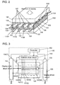
- Fig. 2 is a sectional and perspective view illustrating parts of an image display area of the PDP.
- the numbers of display electrodes, display scanning electrodes and address electrodes are partially omitted for better understanding.
- PDP 100 comprises the following elements:
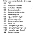
- a structure of PDP 100 is shown in Fig. 2, i.e., on a main face of front glass plate 101, a front panel is prepared, which comprises display electrodes 103, display scanning electrodes 104 and dielectric glass layer 105 and protective film 106 made of MgO.
- a rear panel is prepared, which comprises address electrodes 107, dielectric glass layer 108, partition wall 109, and phosphor layers 110R, 110G, 110B.
- the front and rear panels thus formed are overlapped with each other, and discharge gas is enclosed in discharging space 122 formed between the panels.
- the PDP thus constructed is coupled to PDP driver 150 to work as a plasma display device.
- PDP 100 is coupled to display-driver circuit 153, display-scanning driver circuit 154, and address driver circuit 155, as shown in Fig. 3. Then at each one of the cells to be lighted following the control by controller 152, a voltage is applied to both of display-scanning electrode 104 and address electrode 107 for address discharging therebetween. Next, a pulse voltage is applied between display electrode 103 and display scanning electrode 104 for carrying out a maintaining discharge. This maintaining discharge generates ultraviolet ray at the cell, thereby exciting the phosphor layer to emit the light, and lighting the cell. A combination of lighting cells and non-lighting cells of respective colors displays an image.
- the front panel is manufactured in the following way: Prepare N pieces of display electrodes 103 and display scanning electrodes 104 respectively on front glass plate 101 alternately and in parallel with each other to form a striped pattern (in Fig. 2, only two pieces of each are shown.) Then put dielectric glass layer 105 as a cover on glass plate 101 thus prepared, and form protective film 106 made of MgO on the surface of glass layer 105.
- Display electrode 103 and display scanning electrode 104 comprise silver. Those electrodes are formed by applying silver-paste to electrodes by the screen printing method, and baking the electrode silver-pasted.
- Dielectric glass layer 105 is manufactured in the following way: Apply paste including lead-based glass material by the screen printing method, and bake it at a given temperature and for a given time, e.g., at 560°C for 20 minutes, to form the dielectric glass layer of a given thickness (approx. 20 ⁇ m.)
- the paste including the lead-based glass material uses a mixture of e.g., PbO (70 wt%), B 2 O 3 (15 wt%), SiO 2 (10 wt%), Al 2 O 3 (5 wt%) and organic binder (10% ethyl cellulose dissolved in ⁇ terpineol).
- the organic binder is formed by dissolving resin in organic solvent.
- Acrylic resin can be used as the resin other than ethyl cellulose, and butylcarbitol can be used as organic solvent. Further, dispersant such as glyceryl trileate can be mixed with the organic solvent.
- Protective film 106 comprises MgO, and is formed by sputtering or CVD (chemical vapor deposition) method to have a given thickness (approx. 0.5 ⁇ m.)
- the rear panel is manufactured in the following way: first, screen-print the silver paste, to be used for electrode, on rear-glass panel 102, then bake it, thereby arranging M pieces of address electrodes 107 on plate 102. On top of that, apply the paste containing lead-based glass material by the screen-printing method, thereby forming dielectric glass layer 108. Then apply the paste containing lead-based glass material by the screen-printing method at given pitches repeatedly, thereby forming partition wall 109. This partition wall 109 partitions discharging space 122 into individual cells (a unit of light-emission area) along the line.
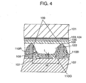
- Fig. 4 is a sectional view of a PDP, and as shown in Fig. 4, an interval between partition walls 109 is specified gener ally at 130 ⁇ m - 240 ⁇ m following a given screen-size of HDTV, such as 32 inches - 50 inches.
- a thickness L of those layers above address electrode 107 is preferably set at approx. 8 - 25 times of the average particle-diameter of the phosphor particles of respective colors.
- those phosphor layers preferably have a thickness corresponding to min. 8 layers of phosphor-particle and more preferably 20 layers in order to obtain an enough brightness (efficiency of light emission) in irradiating the phosphor layer with a given amount of ultraviolet ray. Because the ultraviolet ray generated in the discharging space is preferably absorbed by the phosphor layer instead of permeating the layer.
- the front panel and the rear panel thus manufactured are overlapped with each other such that the respective electrodes on the front panel intersect the address electrodes of the rear panel at right angles.
- sealing glass is prepared at the peripheral of the panel, and baked at approx. 450°C for 10 - 20 minutes to form airtight sealing layer 121, so that both the panels are sealed.
- Discharging space 122 is temporarily evacuated to become high vacuum, e.g., 1.1 ⁇ 10 -4 Pa, then a charging gas such as He - Xe based, or Ne - Xe based inert-gas is filled by a given pressure, thereby producing PDP 100.
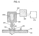
- Fig. 5 shows a schematic structure of an ink applicator to be used for forming the phosphor layer.
- ink applicator 200 comprises server 210, pressure pump 220 and header 230.
- the phosphor ink supplied from server 210 is pressurized by pressure pump 220 and supplied to header 230.
- Header 230 has ink-chamber 230a and nozzle 240.
- the pressurized ink is supplied to ink chamber 230a, and then sequentially ejected from nozzle 240.
- Diameter D of nozzle 240 is preferably not smaller than 30 ⁇ m in order to avoid clogging, and not greater than interval W (approx. 130 - 200 ⁇ m) between partition walls 109 in order to prevent the ink from squeezing out from the partition walls at application.
- Diameter D is generally set at 30 - 130 ⁇ m.
- Header 230 is driven linearly by a header scanning mechanism (not shown), and scanning of header 230 together with ejecting of phosphor ink 250 sequentially from nozzle 240 allow applying the ink uniformly into the grooves between partition walls 109 on rear-glass plate 102.
- the viscosity of the ink is kept in the range of 1,500 - 50,000 centipoise (CP) at 25°C.
- Server 210 is equipped with an agitator (not shown), which prevents the particles in the phosphor ink from being deposited.
- Header 230 together with ink-chamber 230a and nozzle 240 are molded in one piece, and produced by machining and electrical charging a metallic material.
- the method of forming the phosphor layer is not limited to the methods discussed above, for instance, various methods such as photo-litho method, screen-printing method, and the method of arranging films in which phosphor particles are mixed, can be used.
- the phosphor ink is manufactured by mixing phosphor particles of respective colors, binder and solvent, then blending the mixture to be at 1,500-50,000 CP, and adding surface-active agent, silica, or dispersant (0.1 wt% - 5 wt%) if necessary.
- the red phosphor to be blended in this phosphor ink uses a chemical compound such as (Y, Gd) 1 - X BO 3 :Eu X , or Y 2 - X O 3 :Eu X .
- a part of Y element which is one of the elements of the base material, is replaced with Eu, and the replacing amount X of element Eu with respect to element Y preferably falls within 0.05 ⁇ X ⁇ 0.20.
- a greater replacing amount than this range would increase the brightness; however, accelerate substantially the deterioration in brightness, so that it is hard to use this one practically.
- a smaller replacing amount than this X would lower the composition ratio of Eu, which is a major element for light emission, so that the brightness is lowered and the phosphor becomes useless.
- the green phosphor uses a chemical compound such as (Zn 1 - X Mn X ) 2 SiO 4 of which surface is positively charged.
- a part of Zn which is one of the elements of the base material, is replaced with Mn.
- the replacing amount X of element Mn with respect to element Zn preferably falls within 0.01 ⁇ X ⁇ 0.20.
- the blue phosphor uses a chemical compound such as Ba 1-X MgAl 10 O 17 :Eu X or Ba 1-X-Y Sr Y MgAl 10 O 17 :Eu X .
- a part of Ba which is one of the elements of the base material, is replaced with Eu or Sr.
- the replacing amount X of element Eu with respect to element Ba preferably falls within 0.03 ⁇ X ⁇ 0.20, for the first one and 0.1 ⁇ X ⁇ 0.5 for the second one because of the same reason discussed above.
- the binder blended in the phosphor ink uses ethyl-cellulose or acrylic resin (0.1 wt% - 10 wt% of the ink), and the solvent uses ⁇ terpineol or butylcarbitol.
- the binder can also use high polymer such as PMA, PVA, and the solvent also can use organic solvent such as diethylene glycol, methyl ether.
- the phosphor particles manufactured by the solid-phase reaction method, water solution method, spray and bake method, or hydrothermal synthesis method, are used.
- aqueous medium preferably uses ion-exchanged water or pure water because they do not contain impurity, however, they are still usable if they contain non-aqueous solvent such as methanol, ethanol.
- hydration mixed liquid into a vessel made of corrosion resistant and heat resistant material such as gold or platinum, then use a device, which can pressurize and heat a subject at the same time, such as an autoclave, so that the hydration mixed liquid undergoes hydrothermal synthesis in the highly pressurized vessel at a given temperature (100°C - 300°C) and at a given pressure (0.2 Mpa - 10 Mpa) for 12 - 20 hours.
- the phosphor particles obtained through the hydrothermal synthesis are spherical in shape, and an average particle-diameter is as small as 0.05 ⁇ m-2.0 ⁇ m, which is smaller than that of the particles manufactured by the conventional solid-phase reaction method.
- the "spherical shape" used in this embodiment defines the ratio of shorter axis vs. longer axis falls within e.g., 0.9 - 1.0, however, all the particles do not necessarily meet this definition.
- the foregoing hydration mixed liquid may not be put in the vessel made of gold or platinum, but the blue phosphor can be manufactured by the spray method, i.e., the hydration mixed liquid is sprayed from a nozzle into a heated oven.
- This phosphor is different in material from the foregoing Ba 1-X MgAl 10 O 17 :Eu X and is manufactured by the same solid-phase reaction method. The material of this phosphor is described hereinafter.
- a reducing atmosphere e.g., the atmosphere including 5% of hydrogen and 95% of nitrogen
- an air classifier e.g., the atmosphere including 5% of hydrogen and 95% of nitrogen
- oxide, nitrate, and hydroxide are mainly used as the materials; however, organometallic compound, e.g., alkoxide or acetylacetone, which contain chemical elements such as Ba, Sr, Mg, Al, and Eu, can be used as a material of the phosphor.
- hydrothermal synthesis method is used.
- mix the materials at a molar ratio of Zn 1-x Mn x : SiO 2 2 : 3, which exceeds the theoretical mixture ratio in SiO 2 , and put this mixture into ion-exchanged water to produce the mixed liquid.
- the phosphor particles obtained through the hydrothermal synthesis are spherical in shape, and an average particle-diameter is as small as 0.1 ⁇ m - 2.0 ⁇ m. Then bake this powder in the air at 1100 - 1300°C to produce the green phosphor negatively charged. The particle diameter increases to 5 - 15 ⁇ m at this time, and crush this powder with a jet mill into powder of which average particle diameter is 0.1 - 3 ⁇ m. Provide those particles with heat treatment at 400 - 1000'C in nitrogen or nitrogen-oxygen, so that green phosphor positively charged is manufactured.
- the powder is baked at 1100 - 1300°C and lightly crushed before classified into power having particle diameter of 1 - 3 ⁇ m, i.e., (Zn 1-x Mn x ) 2 SiO 4 negatively charged.
- (Zn 1-x Mn x ) 2 SiO 4 negatively charged is coated with MgO; however, Al 2 O 3 , ZnO, Y 2 O 3 , or MgAl 2 O 4 can be used instead of MgO.
- Organometallic compound alkoxide compound, acetylacetone compound, hydrocarbon compound
- non-aqueous solution alcohol, benzene, cyclohxane
- the step of producing a mixed liquid mix the materials such as yttrium nitrate Y 2 (NO 3 ) 2 , and europium nitrate Eu 2 (NO 3 ) 2 , and dissolve this mixture into ion-exchanged water so that the molar ratio becomes 2 - X : X (0.05 ⁇ X ⁇ 0.30).
- the hydration step add basic-water solution, e.g., ammonia water solution, thereby forming hydration.
- the phosphor obtained through the hydrothermal synthesis step has spherical particles of which diameters fall within 0.1- 2.0 ⁇ m, which is fit to form a phosphor layer of excellent light-emission characteristics.
- Samples in accordance with the foregoing embodiment are produced for evaluating the PDP of the present invention, and the following experiments are carried out on the samples:
- Discharging gas is filled by a given pressure into the discharging space and contains neon gas predominantly and 5% of xenon gas.
- Samples of PDP 1 through PDP 10 employ the green phosphor particles which are produced in the following way: Crush the particles of (Zn 1-x Mn x ) 2 SiO 4 negatively charged before annealing, or coat the phosphor of (Zn 1-x Mn x ) 2 SiO 4 with oxide positively charged.
- Table 1 shows synthesis conditions of each sample.
- Amount X of Eu Mfg. method Amount X of Eu Mfg.
- Samples 1 - 4 are formed of the following materials mixed with each other:
- the green phosphor uses (Zn 1-x Mn x ) 2 SiO 4 positively charged by crushing the green phosphor negatively charged, the red phosphor uses (Y, Gd) 1 - X BO 3 : Eu X , and the blue phosphor uses Ba 1-X MgAl 10 O 17 :Eu X .
- the following factors are changed as shown in table 1: methods of synthesizing the phosphor, replacement ratio of Mn vs. Eu which work as the main role of light-emission, in other words, replacement ratio of Mn vs. Zn, and particle diameters before and after the crush only in the case of the green phosphor.
- Samples 5 - 10 are formed of the following materials mixed with each other:
- the red phosphor uses Y 2 - X O 3 : Eux
- the green phosphor uses (Zn 1-x Mn x ) 2 SiO 4 coated with oxide positively charged
- the blue phosphor uses Ba 1 - X - Y Sr Y MgAl 10 O 17 : Eu X .
- the following factors are changed in table 1: methods of synthesizing the phosphor, and in the case of green color, kinds of oxides to be used for coating the (Zn 1-x Mn x ) 2 SiO 4 , and a thickness of those oxides.
- the phosphor ink used to form the phosphor layer, employs the respective phosphor particles shown in table 1, and manufactured by mixing the phosphor, resin, solvent and dispersant. During the manufacturing, the viscosity of each one of the respective phosphor inks is kept in the range of 1,500 CP - 50,000 CP at 25°C. It is observed that the respective phosphor layers include the partition walls uniformly painted with the phosphor ink. A nozzle of 100 ⁇ m diameter is used, and phosphor particles, of which average diameter falls within 0.1 - 3.0 ⁇ m and max. diameter is not greater than 8 ⁇ m, are used in the respective samples.
- Sample No. 11 uses conventional green phosphor-particles of which surface is negatively charged for forming its green phosphor layer.
- a brightness of the panel obtained after the step of manufacturing the panel is measured with a luminance meter when the panel displays white overall, and when the panel displays green.
- a change rate of deterioration in the brightness at the overall-white display and the green display is measured in the following way. Apply 200V to the plasma display device, and apply discharge-maintaining pulses of 50 kHz for 200 hours continuously, and measure the brightness before and after the application of the pulses to find the change rate of deterioration in the brightness, namely, (brightness after the pulse application - brightness before the pulse application) / brightness before the pulse application X 100 is calculated.
- An address error in address discharging is determined by watching an image on the screen, and if flicker is found even in one place, it is determined that an error occurs.
- Table 2 shows the results of experiments 1 - 4, i.e., brightness of green, change rate of deterioration in the brightness of green, and clogging in the nozzle.
- Sample No. Amount of charges to phosphor by blow-off method Brightness of green phosphor on panel Change rate of brightness before and after applying pulses of 200V,50kHz
- comparison sample 11 employing (Zn 1-x Mn x ) 2 SiO 4 negatively charged, as it is, used in the panel shows a greater change-rate of deterioration in green brightness at the accelerated life test because it is negatively charged.
- sample 11 shows the change rate of - 20.5%.
- Samples 1 - 10 which use the green phosphor positively charged, on the other hand, show the change rates as low as between - 2.0% and - 2.4% in all-white display. While sample 11 shows the change rate at - 15.6% in green display, samples 1-10 show their changes rates between - 0.3% and - 1.4%, and yet, no address errors or no clogging in applying the phosphor are found.
- the green phosphor of (Zn 1-x Mn x ) 2 SiO 4 which is one of the elements of the phosphor layer, is positively charged.
- Phosphor particles of which green phosphor crystals are positively or zero charged, are used for forming the green phosphor layer, so that the phosphor layer uniformly applied is obtainable, and deterioration in brightness can be prevented. At the same time, the brightness, service life, and reliability of the PDP can be improved.
Landscapes
- Chemical & Material Sciences (AREA)
- Engineering & Computer Science (AREA)
- Materials Engineering (AREA)
- Organic Chemistry (AREA)
- Inorganic Chemistry (AREA)
- Life Sciences & Earth Sciences (AREA)
- Wood Science & Technology (AREA)
- Manufacturing & Machinery (AREA)
- Physics & Mathematics (AREA)
- Plasma & Fusion (AREA)
- Luminescent Compositions (AREA)
- Gas-Filled Discharge Tubes (AREA)
- Pigments, Carbon Blacks, Or Wood Stains (AREA)
- Inks, Pencil-Leads, Or Crayons (AREA)
Abstract
Description
| Sample No. | Green phosphor (Zn1-xMnx)2SiO4 | Red phosphor (Y,Gd)1-xBO3:Eux | Blue phosphor Ba1-xMgAl10O17:Eu | ||||
| Amount X of Mn | Particle diameter reduced by crush | Coating material and its thickness | Amount X of Eu | Mfg. method | Amount X of Eu | Mfg. method | |
| 1 | X=0.01 | ×0.9 | No coating | X=0.1 | Solid-phase reaction | X=0.03 | Hydrothermal synthesis |
| 2 | X=0.05 | ×0.5 | " | X=0.2 | " | X=0.05 | " |
| 3 | X=0.1 | ×0.1 | " | X=0.3 | " | X=0.1 | " |
| 4 | X=0.2 | ×0.2 | " | X=0.15 | " | X=0.2 | " |
| Green phosphor (Zn1-xMnx)2SiO4 | Red phosphor (Y1-x)2O3:Eux | Blue phosphor Ba1-x-yAl10O17:Eux | |||||
| 5 | X=0.03 | No crush | Al2O3 3nm | X=0.01 | Hydrothermal synthesis | X=0.03 y=0.1 | Solid-phase reaction |
| 6 | X=0.1 | " | ZnO 5nm | X=0.1 | " | X=0.1 y=0.3 | " |
| 7 | X=0.1 | " | MgO 10nm | X=0.15 | Water solution | X=0.1 y=0.5 | " |
| 8 | X=0.2 | " | Y203 6nm | X=0.2 | Solid-phase reaction | X=0.2 y=0.3 | " |
| 9 | " | " | Al2O3 5nm | " | " | " | " |
| 10 | X=0.1 | ×0.5 | Al2O3 10nm | X=0.15 | " | X=0.1 y=0.5 | " |
| 11 | " | No crush | No coating | " | " | " | " |
| Sample No. | Amount of charges to phosphor by blow-off method | Brightness of green phosphor on panel | Change rate of brightness before and after applying pulses of 200V,50kHz | Address error in address discharging | Clogging test by applying green ink through the nozzle for 100 hours continuously | |
| Green | Green | Overall | Green | |||
| 1 | +0.01 | 250 | -2.2 | -1.4 | N/A | No clogging |
| 2 | +0.03 | 258 | -2.1 | -1.0 | " | " |
| 3 | +0.15 | 232 | -2.2 | -0.9 | " | " |
| 4 | +0.10 | 240 | -2.0 | -0.8 | " | " |
| 5 | 0.0 | 248 | -2.2 | -1.1 | " | " |
| 6 | +0.04 | 245 | -2.3 | -1.0 | " | " |
| 7 | +0.06 | 243 | -2.1 | -1.2 | " | " |
| 8 | +0.02 | 237 | -2.3 | -1.1 | " | " |
| 9 | +0.05 | 230 | -2.4 | -1.2 | " | " |
| 10 | +0.5 | 250 | -2.0 | -0.3 | " | " |
| 11 | -1.5 | 205 | -20.5 | -15.6 | Error | Error in 4 hours |
Claims (14)
- A method of manufacturing a plasma display device including a plasma display panel, which comprises:wherein phosphors forming the layers are excited by ultraviolet ray to emit a light, anda plurality of discharging cells arranged and assigned to one or a plurality of colors; andphosphor layers assigned to respective colors corresponding to the colors of the cells,
wherein at least one of the phosphor layers has a green phosphor layer which includes a crystal structure of green phosphor of Zn2SiO4:Mn and has zero or positive charges,
the method applying green phosphor ink, of which major ingredient is the green phosphor, through a nozzle to the discharging cells for forming the green phosphor layer. - The method of manufacturing a plasma display device of claim 1, wherein the green phosphor ink is formed of a mixed liquid comprising:phosphor powder coated with oxide positively charged and having a crystal structure of Zn2SiO4:Mn;resin component comprising ethyl-cellulose; andsolvent component comprising at least one of terpineol, butylcarbitol-acetate, and pentanediol.
- The method of manufacturing a plasma display device of claim 1, wherein the green phosphor ink is formed of a mixed liquid comprising:phosphor powder positively charged by crushing phosphor powder having a crystal structure of Zn2SiO4:Mn such that a surface of the crystal is broken up;resin component comprising ethyl-cellulose; andsolvent component comprising at least one of terpineol, butylcarbitol-acetate, and pentanediol.
- The method of manufacturing a plasma display device of claim 2, wherein the oxide positively charged is one of MgO, ZnO, Y2O3, Al2O3, and MgAl2O4.
- The method of manufacturing a plasma display device of claim 2, wherein the oxide positively charged coats the phosphor powder in a thickness of not greater than 10 nm.
- The method of manufacturing a plasma display device of claim 3 including the steps of:crushing the phosphor, of which surface is negatively charged, having a crystal structure of Zn2SiO4:Mn; andproviding the crushed phosphor with heat treatment at 400-1,000°C.
- A plasma display device comprising:wherein phosphors forming the layers are excited by ultraviolet ray to emit a light,a plasma display panel including:a plurality of discharging cells arranged and assigned to one or a plurality of colors; andphosphor layers assigned to respective colors corresponding to the colors of the cells,
wherein at least one of the phosphor layers is formed of a green phosphor layer which includes a crystal structure of green phosphor of Zn2SiO4:Mn, and
wherein the green phosphor is coated with one of MgO, ZnO, Y2O3, Al2O3, and MgAl2O4 having positive charges in a thickness of not greater than 10 nm. - A plasma display device comprising:wherein phosphors forming the layers are excited by ultraviolet ray to emit a light,a plasma display panel including:a plurality of discharging cells arranged assigned to one or a plurality of colors; andphosphor layers assigned to respective colors corresponding to the colors of the cells,
wherein at least one of the phosphor layers is formed of a green phosphor layer which includes a crystal structure of green phosphor of Zn2SiO4:Mn, and
wherein the green phosphor is produced by crushing Zn2SiO4:Mn having negative charges, so that the Zn2SiO4:Mn is changed to have positive charges. - Phosphor ink to be used in a plasma display device, the ink being formed of a mixed liquid comprising:phosphor powder, originally charged negatively and having crystal structure of Zn2SiO4:Mn, crushed such that a surface of the crystal is broken up and charged positively;resin component comprising ethyl-cellulose; andsolvent component comprising at least one of terpineol, butylcarbitol-acetate, and pentanediol.
- Phosphor ink to be used in a plasma display device, the ink being formed of a mixed liquid comprising:phosphor powder, having a crystal structure of Zn2SiO4:Mn, coated with oxide having positive charges;resin component comprising ethyl-cellulose; andsolvent component comprising at least one of terpineol, butylcarbitol-acetate, and pentanediol.
- The phosphor ink of claim 10, wherein the oxide having positive charges is one of MgO, ZnO, Y2O3, Al2O3, and MgAl2O4.
- The phosphor ink of claim 10, wherein the oxide coats the Zn2SiO4:Mn in a thickness of not greater than 10 nm.
- A method of manufacturing phosphor, the method comprising the steps of:producing a mixed liquid by mixing water with one of metallic salt, oxide and organometallic salt which include ingredients of green phosphor such as Zn, Si, and Mn, wherein amount of Zn with respect to Si is greater than a theoretical mixture ratio;producing the green phosphor having a crystal structure of Zn2SiO4:Mn by drying the mixed liquid and baking the dried product at 1100-1300°C;crushing the green phosphor; andannealing the crushed phosphor at 400 - 1000'C in one of nitrogen and nitrogen-oxygen.
- A method of manufacturing phosphor, the method comprising the steps of:producing a mixed liquid of phosphor material by mixing aqueous medium with one of nitrate compound and oxide which are materials of phosphor having a crystal structure of Zn2SiO4:Mn;producing hydration by mixing the mixed liquid of phosphor material with basic water solution;providing a solution, in which the hydration is mixed with alkaline water, with hydrothermal synthesis reaction in a condition of a temperature at 100 - 350°C and with a pressure of 0.2 Mpa - 25 Mpa;baking the synthesized product at 1100 - 1300°C;classifying the baked product into phosphor having a particle-diameter falling within 5 - 10 µm; andcrushing the classified phosphor with one of a ball mill or a jet mill such that the particle-diameter is reduced to 0.9 - 0.1 times of the classified phosphor.
Applications Claiming Priority (3)
| Application Number | Priority Date | Filing Date | Title |
|---|---|---|---|
| JP2001391453 | 2001-12-25 | ||
| JP2001391453A JP2003183650A (en) | 2001-12-25 | 2001-12-25 | Manufacturing method of plasma display device |
| PCT/JP2002/013360 WO2003056596A1 (en) | 2001-12-25 | 2002-12-20 | Plasma display device and production method therefor |
Publications (2)
| Publication Number | Publication Date |
|---|---|
| EP1383153A1 true EP1383153A1 (en) | 2004-01-21 |
| EP1383153A4 EP1383153A4 (en) | 2009-02-18 |
Family
ID=19188523
Family Applications (1)
| Application Number | Title | Priority Date | Filing Date |
|---|---|---|---|
| EP02786169A Withdrawn EP1383153A4 (en) | 2001-12-25 | 2002-12-20 | PLASMA SCREEN DEVICE AND CORRESPONDING PRODUCTION METHOD |
Country Status (6)
| Country | Link |
|---|---|
| US (1) | US7232530B2 (en) |
| EP (1) | EP1383153A4 (en) |
| JP (1) | JP2003183650A (en) |
| KR (2) | KR100547308B1 (en) |
| CN (1) | CN100440417C (en) |
| WO (1) | WO2003056596A1 (en) |
Cited By (7)
| Publication number | Priority date | Publication date | Assignee | Title |
|---|---|---|---|---|
| EP1717292A2 (en) | 2005-04-20 | 2006-11-02 | Samsung SDI Co., Ltd. | Phosphor composition for plasma display panel, and plasma display panel having phosphor layer composed of the phosphor composition |
| EP1849848A1 (en) | 2006-04-26 | 2007-10-31 | Samsung SDI Co., Ltd. | Phosphor for plasma display panel and plasma display panel including the same |
| EP1890311A4 (en) * | 2006-02-23 | 2008-08-20 | Matsushita Electric Industrial Co Ltd | PLASMA INDICATOR AND METHOD FOR PRODUCING A MATERIAL FROM GREEN PHOSPHORUS FOR THE PLASMA INDICATOR |
| EP1619231A4 (en) * | 2003-04-22 | 2010-02-10 | Panasonic Corp | LUMINOPHORE AND PLASMA DISPLAY UNIT |
| EP1860676A4 (en) * | 2006-02-23 | 2010-07-14 | Panasonic Corp | PLASMA DISPLAY DEVICE AND METHOD FOR MANUFACTURING GREEN PHOSPHORUS FOR SAID DISPLAY DEVICE |
| EP1865529A4 (en) * | 2006-02-23 | 2011-03-09 | Panasonic Corp | PLASMA INDICATOR AND METHOD FOR PRODUCING A MATERIAL FROM GREEN PHOSPHORUS FOR THE PLASMA INDICATOR |
| EP1865528A4 (en) * | 2006-02-23 | 2011-03-09 | Panasonic Corp | PLASMA INDICATOR AND METHOD FOR PRODUCING A MATERIAL FROM GREEN PHOSPHORUS FOR THE PLASMA INDICATOR |
Families Citing this family (27)
| Publication number | Priority date | Publication date | Assignee | Title |
|---|---|---|---|---|
| JP4449389B2 (en) | 2003-09-26 | 2010-04-14 | パナソニック株式会社 | Method for manufacturing phosphor for plasma display device |
| KR100589404B1 (en) * | 2004-01-26 | 2006-06-14 | 삼성에스디아이 주식회사 | Green phosphor for plasma display panel and plasma display panel comprising same |
| US20050170073A1 (en) * | 2004-01-30 | 2005-08-04 | Teco Nanotech Co., Ltd. | Phosphors spray and method for spraying the same |
| JP2005350657A (en) * | 2004-05-11 | 2005-12-22 | Matsushita Electric Ind Co Ltd | Phosphor and plasma display panel using the phosphor |
| JP2006008767A (en) * | 2004-05-21 | 2006-01-12 | Konica Minolta Holdings Inc | Method for producing phosphor |
| US7270774B2 (en) * | 2004-05-26 | 2007-09-18 | Matsushita Electric Industrial Co., Ltd. | Phosphor having resistance to deterioration caused by ultraviolet rays, and gas discharge display device of which image quality is not readily deteriorated over time |
| WO2005118745A1 (en) * | 2004-06-02 | 2005-12-15 | Konica Minolta Holdings, Inc. | Manganese-activated zinc silicate phosphor and plasma display panel |
| KR100659062B1 (en) * | 2004-10-11 | 2006-12-19 | 삼성에스디아이 주식회사 | Phosphor paste composition and manufacturing method of flat panel display device using same |
| EP1854862A1 (en) * | 2005-02-28 | 2007-11-14 | Konica Minolta Medical & Graphic, Inc. | Fluorescent body and plasma display panel |
| KR20060097146A (en) * | 2005-03-04 | 2006-09-14 | 삼성에스디아이 주식회사 | Green phosphor composition for plasma display panel and plasma display panel manufactured therefrom |
| JPWO2006109396A1 (en) * | 2005-03-30 | 2008-10-09 | コニカミノルタエムジー株式会社 | Phosphor production method and phosphor |
| CN100485851C (en) * | 2005-07-27 | 2009-05-06 | 鸿富锦精密工业(深圳)有限公司 | Plasma display |
| JP2007103052A (en) * | 2005-09-30 | 2007-04-19 | Matsushita Electric Ind Co Ltd | Plasma display panel |
| KR100730216B1 (en) * | 2006-03-28 | 2007-06-19 | 삼성에스디아이 주식회사 | Plasma display panel |
| US7612502B2 (en) * | 2006-06-01 | 2009-11-03 | Chunghwa Picture Tubes, Ltd. | Planar light source |
| US7841918B2 (en) * | 2006-12-15 | 2010-11-30 | Chunghwa Picture Tubes, Ltd. | Method for manufacturing plane light source |
| KR20090003674A (en) * | 2007-07-03 | 2009-01-12 | 엘지전자 주식회사 | Plasma display panel |
| KR100932984B1 (en) * | 2008-02-01 | 2009-12-21 | 삼성에스디아이 주식회사 | Red phosphor for display device and display device comprising same |
| KR20090096150A (en) * | 2008-03-07 | 2009-09-10 | 삼성에스디아이 주식회사 | Plasma display panel positioned of phosphors layers having the same zeta potential each other |
| KR100968639B1 (en) * | 2008-06-02 | 2010-07-06 | 박수길 | A sectional hair rod |
| JP2010146741A (en) * | 2008-12-16 | 2010-07-01 | Hitachi Plasma Display Ltd | Plasma display panel |
| KR101053884B1 (en) * | 2008-12-17 | 2011-08-04 | 삼성에스디아이 주식회사 | A composition for forming a phosphor layer, a plasma display panel, and a method of manufacturing the plasma display panel |
| US20110163657A1 (en) * | 2009-05-25 | 2011-07-07 | Panasonic Corporation | Phosphor, method for producing the same, and light-emitting device |
| US20130069520A1 (en) * | 2011-02-24 | 2013-03-21 | Panasonic Corporation | Plasma-display panel |
| US20130069521A1 (en) * | 2011-02-24 | 2013-03-21 | Panasonic Corporation | Plasma-display panel |
| CN102766453B (en) * | 2012-06-29 | 2014-04-02 | 彩虹集团电子股份有限公司 | Surface treatment method for silicic acid zinc-manganese green fluorescent powder applicable to PDP |
| US9166158B2 (en) | 2013-02-25 | 2015-10-20 | Micron Technology, Inc. | Apparatuses including electrodes having a conductive barrier material and methods of forming same |
Family Cites Families (15)
| Publication number | Priority date | Publication date | Assignee | Title |
|---|---|---|---|---|
| US5196234A (en) * | 1986-08-29 | 1993-03-23 | Gte Products Corporation | Method for preparing zinc orthosilicate phosphor particle |
| US4925703A (en) * | 1988-12-22 | 1990-05-15 | Gte Products Corporation | Firing and milling method for producing a manganese activated zinc silicate phosphor |
| JPH0766744B2 (en) * | 1989-10-17 | 1995-07-19 | 日亜化学工業株式会社 | DC type plasma display panel |
| JP2653576B2 (en) * | 1990-08-31 | 1997-09-17 | 株式会社東芝 | Low pressure mercury vapor discharge lamp |
| JP3302080B2 (en) | 1993-03-19 | 2002-07-15 | 株式会社東芝 | Automatic analyzer |
| FR2742161B1 (en) * | 1995-12-08 | 1998-01-09 | Thomson Csf | PROCESS FOR PRODUCING A LUMINOPHORE |
| JPH10195428A (en) * | 1997-01-16 | 1998-07-28 | Toshiba Corp | Phosphor particles, method for producing the same, and plasma display panel |
| JP3587661B2 (en) * | 1997-09-12 | 2004-11-10 | 富士通株式会社 | Plasma display panel |
| JPH11293239A (en) * | 1998-04-13 | 1999-10-26 | Kansai Shingijutsu Kenkyusho:Kk | Image display device and method of manufacturing the same |
| US6547617B1 (en) * | 1998-07-08 | 2003-04-15 | Hiroyuki Kawamura | Plasma display panel manufacturing method for manufacturing a plasma display panel with superior picture quality, a manufacturing apparatus and a phosphor ink |
| JP3236837B2 (en) * | 1998-07-08 | 2001-12-10 | 松下電器産業株式会社 | Method and apparatus for manufacturing plasma display panel |
| JP3296301B2 (en) * | 1998-09-11 | 2002-06-24 | 松下電器産業株式会社 | Method for forming phosphor layer and method for manufacturing plasma display panel using the same |
| JP2000230173A (en) * | 1999-02-10 | 2000-08-22 | Matsushita Electric Ind Co Ltd | Method for manufacturing phosphor for plasma display, method for manufacturing plasma display panel, and plasma display panel |
| JP2001187884A (en) * | 1999-10-19 | 2001-07-10 | Matsushita Electric Ind Co Ltd | Method for manufacturing phosphor, plasma display panel display device, and fluorescent lamp |
| JP3797084B2 (en) | 1999-12-14 | 2006-07-12 | 松下電器産業株式会社 | Plasma display device |
-
2001
- 2001-12-25 JP JP2001391453A patent/JP2003183650A/en active Pending
-
2002
- 2002-12-20 CN CNB028099788A patent/CN100440417C/en not_active Expired - Fee Related
- 2002-12-20 WO PCT/JP2002/013360 patent/WO2003056596A1/en not_active Ceased
- 2002-12-20 EP EP02786169A patent/EP1383153A4/en not_active Withdrawn
- 2002-12-20 KR KR20037014267A patent/KR100547308B1/en not_active Expired - Fee Related
- 2002-12-20 KR KR1020057022215A patent/KR100803467B1/en not_active Expired - Fee Related
- 2002-12-20 US US10/476,691 patent/US7232530B2/en not_active Expired - Fee Related
Cited By (11)
| Publication number | Priority date | Publication date | Assignee | Title |
|---|---|---|---|---|
| EP1619231A4 (en) * | 2003-04-22 | 2010-02-10 | Panasonic Corp | LUMINOPHORE AND PLASMA DISPLAY UNIT |
| EP1717292A2 (en) | 2005-04-20 | 2006-11-02 | Samsung SDI Co., Ltd. | Phosphor composition for plasma display panel, and plasma display panel having phosphor layer composed of the phosphor composition |
| EP1717292A3 (en) * | 2005-04-20 | 2007-06-27 | Samsung SDI Co., Ltd. | Phosphor composition for plasma display panel, and plasma display panel having phosphor layer composed of the phosphor composition |
| EP1890311A4 (en) * | 2006-02-23 | 2008-08-20 | Matsushita Electric Industrial Co Ltd | PLASMA INDICATOR AND METHOD FOR PRODUCING A MATERIAL FROM GREEN PHOSPHORUS FOR THE PLASMA INDICATOR |
| US7705537B2 (en) | 2006-02-23 | 2010-04-27 | Panasonic Corporation | Plasma display device |
| EP1860676A4 (en) * | 2006-02-23 | 2010-07-14 | Panasonic Corp | PLASMA DISPLAY DEVICE AND METHOD FOR MANUFACTURING GREEN PHOSPHORUS FOR SAID DISPLAY DEVICE |
| EP1865529A4 (en) * | 2006-02-23 | 2011-03-09 | Panasonic Corp | PLASMA INDICATOR AND METHOD FOR PRODUCING A MATERIAL FROM GREEN PHOSPHORUS FOR THE PLASMA INDICATOR |
| EP1865528A4 (en) * | 2006-02-23 | 2011-03-09 | Panasonic Corp | PLASMA INDICATOR AND METHOD FOR PRODUCING A MATERIAL FROM GREEN PHOSPHORUS FOR THE PLASMA INDICATOR |
| US7911139B2 (en) | 2006-02-23 | 2011-03-22 | Panasonic Corporation | Plasma display device with improved luminance |
| US8035301B2 (en) | 2006-02-23 | 2011-10-11 | Panasonic Corporation | Plasma display device and method of manufacturing green phosphor material for plasma display device |
| EP1849848A1 (en) | 2006-04-26 | 2007-10-31 | Samsung SDI Co., Ltd. | Phosphor for plasma display panel and plasma display panel including the same |
Also Published As
| Publication number | Publication date |
|---|---|
| CN100440417C (en) | 2008-12-03 |
| US20040239245A1 (en) | 2004-12-02 |
| EP1383153A4 (en) | 2009-02-18 |
| KR100803467B1 (en) | 2008-02-14 |
| KR100547308B1 (en) | 2006-01-26 |
| US7232530B2 (en) | 2007-06-19 |
| WO2003056596A1 (en) | 2003-07-10 |
| JP2003183650A (en) | 2003-07-03 |
| KR20050118243A (en) | 2005-12-15 |
| KR20030088514A (en) | 2003-11-19 |
| CN1509488A (en) | 2004-06-30 |
Similar Documents
| Publication | Publication Date | Title |
|---|---|---|
| US7232530B2 (en) | Plasma display device and production method therefor | |
| US7147802B2 (en) | Phosphor and method for production thereof and plasma display device | |
| EP1350829B1 (en) | Fluorescent material, manufacturing method thereof, and plasma display apparatus | |
| EP1426430A1 (en) | PLASMA DISPLAY APPARATUS, FLUORESCENT MATERIAL, AND FLUORESCENT MATERIAL MANUFACTURING METHOD | |
| EP1426431A1 (en) | PLASMA DISPLAY APPARATUS, FLUORESCENT MATERIAL, AND FLUORESCENT MATERIAL MANUFACTURING METHOD | |
| US7423368B2 (en) | Plasma display and method of producing phosphor used therein | |
| US7261917B2 (en) | Plasma display and method of producing phosphor used therein | |
| US7531961B2 (en) | Plasma display with phosphors containing a β-alumina crystal structure | |
| JP2005183246A (en) | Plasma display device | |
| JP4013644B2 (en) | Method for manufacturing plasma display device | |
| JP2004067885A (en) | Plasma display panel | |
| JP2005183245A (en) | Plasma display device | |
| JP2004091623A (en) | Plasma display panel | |
| JP2005100891A (en) | Plasma display device | |
| JP2004067874A (en) | Plasma display panel |
Legal Events
| Date | Code | Title | Description |
|---|---|---|---|
| PUAI | Public reference made under article 153(3) epc to a published international application that has entered the european phase |
Free format text: ORIGINAL CODE: 0009012 |
|
| 17P | Request for examination filed |
Effective date: 20031021 |
|
| AK | Designated contracting states |
Kind code of ref document: A1 Designated state(s): AT BE BG CH CY CZ DE DK EE ES FI FR GB GR IE IT LI LU MC NL PT SE SI SK TR |
|
| RAP1 | Party data changed (applicant data changed or rights of an application transferred) |
Owner name: PANASONIC CORPORATION |
|
| A4 | Supplementary search report drawn up and despatched |
Effective date: 20090121 |
|
| RIC1 | Information provided on ipc code assigned before grant |
Ipc: C09K 11/08 20060101ALI20090115BHEP Ipc: H01J 11/02 20060101ALI20090115BHEP Ipc: H01J 9/227 20060101ALI20090115BHEP Ipc: C09K 11/59 20060101AFI20090115BHEP Ipc: C09D 11/00 20060101ALI20090115BHEP |
|
| 17Q | First examination report despatched |
Effective date: 20090406 |
|
| STAA | Information on the status of an ep patent application or granted ep patent |
Free format text: STATUS: THE APPLICATION IS DEEMED TO BE WITHDRAWN |
|
| 18D | Application deemed to be withdrawn |
Effective date: 20120630 |