EP1381121A2 - Anordnung zum Schutz vor elektrostatischen und elektromagnetischen Störungen - Google Patents
Anordnung zum Schutz vor elektrostatischen und elektromagnetischen Störungen Download PDFInfo
- Publication number
- EP1381121A2 EP1381121A2 EP03015215A EP03015215A EP1381121A2 EP 1381121 A2 EP1381121 A2 EP 1381121A2 EP 03015215 A EP03015215 A EP 03015215A EP 03015215 A EP03015215 A EP 03015215A EP 1381121 A2 EP1381121 A2 EP 1381121A2
- Authority
- EP
- European Patent Office
- Prior art keywords
- arrangement according
- contact
- housing part
- housing parts
- housing
- Prior art date
- Legal status (The legal status is an assumption and is not a legal conclusion. Google has not performed a legal analysis and makes no representation as to the accuracy of the status listed.)
- Withdrawn
Links
Images


Classifications
-
- H—ELECTRICITY
- H01—ELECTRIC ELEMENTS
- H01R—ELECTRICALLY-CONDUCTIVE CONNECTIONS; STRUCTURAL ASSOCIATIONS OF A PLURALITY OF MUTUALLY-INSULATED ELECTRICAL CONNECTING ELEMENTS; COUPLING DEVICES; CURRENT COLLECTORS
- H01R13/00—Details of coupling devices of the kinds covered by groups H01R12/70 or H01R24/00 - H01R33/00
- H01R13/648—Protective earth or shield arrangements on coupling devices, e.g. anti-static shielding
- H01R13/6485—Electrostatic discharge protection
-
- H—ELECTRICITY
- H01—ELECTRIC ELEMENTS
- H01R—ELECTRICALLY-CONDUCTIVE CONNECTIONS; STRUCTURAL ASSOCIATIONS OF A PLURALITY OF MUTUALLY-INSULATED ELECTRICAL CONNECTING ELEMENTS; COUPLING DEVICES; CURRENT COLLECTORS
- H01R13/00—Details of coupling devices of the kinds covered by groups H01R12/70 or H01R24/00 - H01R33/00
- H01R13/648—Protective earth or shield arrangements on coupling devices, e.g. anti-static shielding
Definitions
- the invention relates to an arrangement for protection against electrostatic and electromagnetic interference electrical Components in a case at a transition from the first Housing part to another housing part, which is detachable with each other are connected.
- Electrostatic charges harmful to electronic components have their origin both in nature and in the people with electronic components and assemblies work, as well as in items related to manufacturing processes away, more or less quickly. Electrostatic discharges can occur on electronic components Damage that often only occurs in later operation demonstrate. Furthermore, for devices with electronic Component compliance with electromagnetic compatibility. Especially with semiconductor components, their clock frequency Penetrating into the gigahertz range are interference from electromagnetic Observing influences and for that reason to avoid. Assigns an electrical or electronic device a housing that consists of several housing parts, leaks occur at the connections between the housing parts in terms of electromagnetic waves. Likewise, regarding electrostatic discharges Housing parts at these transitions between the housing parts, to observe a contact resistance that is reliable Discharge of the electrostatic charge if possible should be low.
- this is not only based on contacting between the housing parts, but also that the largest possible contact area between the housing parts arises and a, due to manufacturing tolerances, Air gap between the end faces of the housing parts if possible remains low.
- the electromagnetic penetrating into the air gap Waves continue in this until they hit you Contact between the two end faces of the housing parts. Because these contacts between the housing parts on the end faces are random in nature and due to manufacturing tolerances not from a 100% contact on the End faces can be assumed is one according to the invention
- There is angling in the two contact surfaces this causes that the electromagnetic waves at this bend reflected or broken. This also means shielding against 100% contacting electromagnetic fields guaranteed.
- the bend in the two contact surfaces correspond to each other designed so that there is a labyrinth in which the electromagnetic waves are reflected and refracted.
- the shielding against electromagnetic waves can still be improve by adding more bends to the maze is expanded. It is obvious that the quality the shield increases with each bend.
- the invention is not only limited to housing parts, which are made of sheet metal, but is equally functional for housing parts made of solid and in the material thickness stronger components, provided that these are made of electrical conductive metals are made. It is crucial only that the end faces of the housing parts contact as possible and thus electrical contact between the two Housing parts results and that the end faces corresponding Have bends that are like in a labyrinth electromagnetic waves break and before further spread be held.
- contact elements attached to at least one of the two end faces. These contact elements make at predetermined points an electrical contact between the housing parts. It is advantageous to have these contact elements in regular Spread distances across the length of an end face. The choice of the distances between the contact elements is included sometimes also depending on the electromagnetic to be shielded Waves or their wavelengths or the clock frequency.
- one of the housing parts is made of sheet metal, this is a good option the contact elements in an advantageous manner as well to manufacture from this sheet.
- this can be achieved by punching in the manufacturing process of the Housing part, a window around the contact element, so that there is a sheet metal tab for the contact element, the is resiliently arranged in a window of the sheet.
- Um now ensure that the contact is on in a predetermined manner the free end of the contact element takes place on this point of contact in the form attached that the Surface of the contact protrudes beyond the level of the housing part and points in the direction of the other housing part.
- the expression can be achieved by a simple embossing step accomplish and is therefore advantageous over others Manufacturing methods for the contact points.
- contact element in the same plane with the housing part and its end face rests. Thus towers out of this Level only the contact point itself. This advantageously avoids that when assembling the housing parts, contact elements "get caught” or bent adjacent housing parts and their function is impaired.
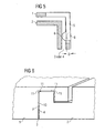
- FIG. 1 shows a detail of a first housing part 1 and a second housing part 2. Since in this case the housing parts are made of sheet metal due to manufacturing tolerances small air gaps 3 between the housing parts difficult or unavoidable. Penetrate this air gap electromagnetic fields or waves. Without further action the electromagnetic waves penetrate at this point or fields through the housing. This results in a Leakage to electromagnetic waves and Fields. To effectively prevent this, the invention provides a corresponding one on the end faces of the housing parts 9 and 10 Angle 11 before. At this angle, the penetrated and broken electromagnetic waves further spread prevented. The illustration shows for the Bends 11 a right angle. It is for the function the invention or the shielding is of secondary importance, what dimension this angle 11 has. Execution in 90 ° has cost advantages in production.
- the Angle 12 between the end faces 9 and 10 and the housing parts 1 and 2 is also shown at 90 ° in the figure. This is a preferred embodiment in view on the manufacture of the housing parts and with regard to the further processing of the housing parts and assembly. It however, other angles are also conceivable at this point.
- Figure 2 shows the arrangement a "Gaskets" 4, instead of the air gap 3. All other variations are also in this embodiment conceivable, as already described in Figure 1.
- FIG. 3 shows a further embodiment of the invention shown, the labyrinth by further bends 11 is expanded.
- the ones already described in FIG. 1 also apply here Variations. It doesn't matter if the Angle as shown in this preferred embodiment are created in 90 °. There are others to each other corresponding angles possible. Again, you can choose between the a "gasket" can be arranged on both end surfaces 9 and 10, the electrical contact between the two end faces increased and the effect of the labyrinth additionally improved.
- Figure 4 shows a preferred embodiment which is essentially Points of Figure 3 is the same. This also instructs a housing part contact elements 5. These contact elements 5 are at regular intervals 7 along the length of the end face 9 attached to the housing part 1. The contact elements are through a stamping process from the sheet metal of the housing part manufactured. They point at the free end of the contact elements 5 an expression in the direction of the other end surface 10. These features 6 provide electrical contact between the two housing parts 1 and 2 safely. The thickness D the contact elements is the thickness of the sheet metal of the housing part equal. Another processing of the contact elements beyond the stamping process and the embossing process, for the formation of the characteristics of the contacts does not take place.
- the contact element 5 has an expression 6, which is characterized by the impression 8 is manufactured in a manufacturing process and also has the same thickness D over the entire length of the contact element on. This ensures that the contact element is at rest apart from the expression 6, no part of the contact element 5 protrudes beyond the level of the housing part 1. So is also ensured that when assembling the housing part no snagging on other housing parts is possible, which in turn to destroy or deform the contact element 5 could lead.
- the shield according to the invention is at the transition between two housing parts 1 and 2 and their end faces 9 and 10, the housing parts 1 and 2 not being shown here are made of sheet metal, but of solid conductive metal.
- the degree of the bends 11 is shown here in 90 °. However, it is any other size of these bends conceivable and possible.
Landscapes
- Shielding Devices Or Components To Electric Or Magnetic Fields (AREA)
Abstract
Description
Claims (16)
- Anordnung zum Schutz vor elektrostatischen und elektromagnetischen Störungen elektronischer Komponenten in einem Gehäuse, bei einem Übergang eines ersten Gehäuseteils (1) zu einem zweiten Gehäuseteil (2), die lösbar miteinander verbunden sind,
dadurch gekennzeichnet, daß
korrespondierende Endflächen (9, 10) der Gehäuseteile (1, 2) eng aneinander liegen, so daß sich auf einer möglichst großen Fläche zwischen den Gehäuseteilen (1, 2) elektrischer Kontakt ergibt, und daß die Endflächen (9, 10) mindestens eine korrespondierende Abwinkelung (11) aufweisen. - Anordnung nach Patentanspruch 1,
dadurch gekennzeichnet, daß
ein Luftspalt (3) zwischen den Gehäuseteilen (1, 2) so gering ist, daß sich auf einer möglichst großen Fläche zwischen den Gehäuseteilen (1, 2) elektrischer Kontakt ergibt. - Anordnung nach Patentanspruch 1 bis 2,
dadurch gekennzeichnet, daß
die Endflächen (9, 10) in einem rechten Winkel zu den Gehäuseteilen (1, 2) stehen. - Anordnung nach einem der vorhergehenden Patentansprüche,
dadurch gekennzeichnet, daß
die Abwinkelung (11) rechtwinkelig ist. - Anordnung nach einem der vorhergehenden Patentansprüche,
dadurch gekennzeichnet, daß
die Profile der Endflächen (9, 10) so formschlüssig sind, daß sich an möglichst vielen Stellen elektrischer Kontakt ergibt. - Anordnung nach einem der vorhergehenden Patentansprüche,
dadurch gekennzeichnet, daß
der Luftspalt (3) mit einer leicht formbaren und elektrisch leitenden Dichtung (4) ausgefüllt ist. - Anordnung nach einem der vorhergehenden Patentansprüche,
dadurch gekennzeichnet, daß
mindestens eines der Gehäuseteile (1, 2) aus Blech geformt ist. - Anordnung nach einem der vorhergehenden Patentansprüche,
dadurch gekennzeichnet, daß
an mindestens einer Endfläche (9, 10) Kontaktelemente (5) angebracht sind, die an der anderen Endfläche elektrisch leitend anliegen. - Anordnung nach Patentanspruch 8,
dadurch gekennzeichnet, daß
die Kontaktelemente (5) entlang der Endfläche (9, 10) in regelmäßigen Abständen (7) zueinander angebracht sind. - Anordnung nach Patentanspruch 8 bis 9,
dadurch gekennzeichnet, daß
zumindest das die Kontaktelemente (5) tragende Gehäuseteil (1 oder 2), aus Blech geformt ist. - Anordnung nach Patentanspruch 10,
dadurch gekennzeichnet, daß
das Kontaktelement (5) eine Blechlasche ist, die einstückig aus dem Blech, des aus Blech geformten Gehäuseteils (1 oder 2) geformt ist. - Anordnung nach Patentanspruch 11,
dadurch gekennzeichnet, daß
das freie Ende des Kontaktelements (5) eine kontaktbildende Ausprägung (6) in Richtung des anderen Gehäuseteiles (1 oder 2) aufweist. - Anordnung nach Patentanspruch 8 bis 12,
dadurch gekennzeichnet, daß
das Kontaktelement (5) federnde Eigenschaften aufweist. - Anordnung nach Patentanspruch 8 bis 13,
dadurch gekennzeichnet, daß
die Stärke D des Kontaktelementes (5) gleich der Stärke des Blechs des Gehäuseteils (1 oder 2) ist. - Anordnung nach Patentanspruch 8 bis 14,
dadurch gekennzeichnet, daß
das Kontaktelement (5) in gleicher Ebene mit dem Blech des Gehäuseteils (1 oder 2) liegt und die Ausprägung (6) in Richtung zu dem anderen Gehäuseteil über die Ebene des Gehäuseteils (1 oder 2) hinausragt. - Anordnung nach Patentanspruch 8 bis 14,
dadurch gekennzeichnet, daß
die Kontaktelemente (5) über die Abwinkelung (11) hinaus angeordnet sind und dabei der Form der Abwinkelung (11) folgen.
Applications Claiming Priority (2)
| Application Number | Priority Date | Filing Date | Title |
|---|---|---|---|
| DE10230902 | 2002-07-09 | ||
| DE10230902A DE10230902A1 (de) | 2002-07-09 | 2002-07-09 | Anordnung zum Schutz vor elektrostatischen und elektromagnetischen Störungen |
Publications (2)
| Publication Number | Publication Date |
|---|---|
| EP1381121A2 true EP1381121A2 (de) | 2004-01-14 |
| EP1381121A3 EP1381121A3 (de) | 2005-11-02 |
Family
ID=29723807
Family Applications (1)
| Application Number | Title | Priority Date | Filing Date |
|---|---|---|---|
| EP03015215A Withdrawn EP1381121A3 (de) | 2002-07-09 | 2003-07-04 | Anordnung zum Schutz vor elektrostatischen und elektromagnetischen Störungen |
Country Status (4)
| Country | Link |
|---|---|
| US (1) | US20040047103A1 (de) |
| EP (1) | EP1381121A3 (de) |
| CN (1) | CN100473267C (de) |
| DE (1) | DE10230902A1 (de) |
Families Citing this family (2)
| Publication number | Priority date | Publication date | Assignee | Title |
|---|---|---|---|---|
| US7063767B1 (en) * | 2002-02-08 | 2006-06-20 | Proteus Technical Solutions, Inc. | Process for creating a durable EMI/RFI shield between two or more structural surfaces and shield formed therefrom |
| DE102012015272A1 (de) | 2012-07-31 | 2014-02-06 | Audi Ag | Verfahren zur effizienten Absicherung sicherheitskritischer Funktionen eines Steuergeräts und Steuergerät |
Family Cites Families (10)
| Publication number | Priority date | Publication date | Assignee | Title |
|---|---|---|---|---|
| FR894795A (fr) * | 1943-05-19 | 1945-01-05 | Bosch Gmbh Robert | Joint électrique étanche pour les boîtiers servant d'écran |
| DE2250639B2 (de) * | 1972-10-16 | 1976-03-18 | Siemens AG, 1000 Berlin und 8000 München | Elektromagnetische abdichtung von verbindungsfugen bei verschraubten schirmungselementen |
| US4769280A (en) * | 1980-12-22 | 1988-09-06 | Chomerics, Inc. | Electromagnetic shielding |
| JPH0282698A (ja) * | 1988-09-20 | 1990-03-23 | Kitagawa Kogyo Kk | 電磁波シールド用部材 |
| DE9103040U1 (de) * | 1991-03-13 | 1991-06-13 | Siemens Nixdorf Informationssysteme AG, 4790 Paderborn | Vorrichtung zur Kontaktierung von Wanne und Haube eines geschlossenen Gehäuses |
| DE9103080U1 (de) * | 1991-03-14 | 1992-07-09 | Philips Patentverwaltung Gmbh, 2000 Hamburg | Abgeschirmtes Gehäuse für elektrische Geräte |
| JP2524471B2 (ja) * | 1993-07-22 | 1996-08-14 | 日本電気株式会社 | Emiガスケット |
| US5532427A (en) * | 1994-10-24 | 1996-07-02 | Gerome Manufacturing Company, Inc. | Electrically conductive joint |
| US6194653B1 (en) * | 1998-03-24 | 2001-02-27 | General Instrument Corporation | Enclosure design having an integrated system of retention, electromagnetic interference containment and structural load distribution |
| US6313400B1 (en) * | 1999-07-13 | 2001-11-06 | Itt Manufacturing Enterprises, Inc. | Data card easily assembled housing |
-
2002
- 2002-07-09 DE DE10230902A patent/DE10230902A1/de not_active Ceased
-
2003
- 2003-07-04 EP EP03015215A patent/EP1381121A3/de not_active Withdrawn
- 2003-07-09 CN CNB031274803A patent/CN100473267C/zh not_active Expired - Fee Related
- 2003-07-09 US US10/616,113 patent/US20040047103A1/en not_active Abandoned
Also Published As
| Publication number | Publication date |
|---|---|
| US20040047103A1 (en) | 2004-03-11 |
| CN100473267C (zh) | 2009-03-25 |
| DE10230902A1 (de) | 2004-02-05 |
| CN1484485A (zh) | 2004-03-24 |
| EP1381121A3 (de) | 2005-11-02 |
Similar Documents
| Publication | Publication Date | Title |
|---|---|---|
| DE102017108433B4 (de) | Halterahmen für einen Steckverbinder und Verfahren zur Bestückung | |
| EP1520457B1 (de) | Abschirmeinrichtung für elektronische baugruppen auf einer leiterplatte | |
| DE102012111184A1 (de) | Radareinrichtung für ein Fahrzeug | |
| EP3488128B1 (de) | Dichtungselement zur fluiddichten und elektrisch leitenden verbindung eines ersten bauteils und eines zweiten bauteils sowie entsprechende bauteilanordnung | |
| DE112018005968T5 (de) | Verbinderanschluss und Verbinder | |
| DE202020101449U1 (de) | Fixierbügel für ein Gehäuse und Gehäuse | |
| EP2478592B1 (de) | Elektrisches kontaktieren eines elektrischen bauteils | |
| WO2004107613A1 (de) | Vorrichtung zum absorbieren des rauschens | |
| EP0952765B1 (de) | Kontaktstreifen zum elektrischen Kontaktieren und/oder zur Erzielung einer gegen hochfrequente elektromagnetische Wellen dichten Verbindung sowie zugehörige Abschirmanordnung | |
| DE10230902A1 (de) | Anordnung zum Schutz vor elektrostatischen und elektromagnetischen Störungen | |
| DE102016211300A1 (de) | Halterahmen für einen Steckverbinder und Verfahren zur Bestückung | |
| DE102008016076B4 (de) | Verbinderschirmung, Verbindersystem und Verwendung | |
| EP4445457A1 (de) | Rückwärtig montierbares steckverbindergehäuse | |
| DE102017111293A1 (de) | Kontaktstift | |
| EP0647986B1 (de) | Kontaktstift für Steckverbindungen | |
| DE29505601U1 (de) | EMV-dichte Gehäuse für schwere Steckverbinder der Serie C146 | |
| EP1579749B1 (de) | Abschirmgehäuse zur Aufnahme einer elektronischen Schaltung | |
| DE112014002199B4 (de) | Elektronische Baugruppe mit einem Kunststoffgehäuse | |
| DE102010025385B4 (de) | Geschirmter Steckverbinder | |
| DE19923705B4 (de) | Elektrische Steckverbindung | |
| DE19544361B4 (de) | Abschirmung für einen elektrischen Stecker und abgeschirmter elektrischer Stecker | |
| DE20219106U1 (de) | Abschirmgehäuse | |
| DE102005033664A1 (de) | Federblech in einem Gehäuse als Abschirmung für ein elektronisches hochfrequenztechnisches Gerät | |
| DE102016105116A1 (de) | Erdungsblechanordnung | |
| DE102014109819A1 (de) | Abschirmgehäuse |
Legal Events
| Date | Code | Title | Description |
|---|---|---|---|
| PUAI | Public reference made under article 153(3) epc to a published international application that has entered the european phase |
Free format text: ORIGINAL CODE: 0009012 |
|
| AK | Designated contracting states |
Kind code of ref document: A2 Designated state(s): AT BE BG CH CY CZ DE DK EE ES FI FR GB GR HU IE IT LI LU MC NL PT RO SE SI SK TR |
|
| AX | Request for extension of the european patent |
Extension state: AL LT LV MK |
|
| RAP1 | Party data changed (applicant data changed or rights of an application transferred) |
Owner name: FUJITSU SIEMENS COMPUTERS GMBH |
|
| PUAL | Search report despatched |
Free format text: ORIGINAL CODE: 0009013 |
|
| AK | Designated contracting states |
Kind code of ref document: A3 Designated state(s): AT BE BG CH CY CZ DE DK EE ES FI FR GB GR HU IE IT LI LU MC NL PT RO SE SI SK TR |
|
| AX | Request for extension of the european patent |
Extension state: AL LT LV MK |
|
| RIC1 | Information provided on ipc code assigned before grant |
Ipc: 7H 05K 9/00 B Ipc: 7H 01R 13/648 A |
|
| 17P | Request for examination filed |
Effective date: 20051222 |
|
| AKX | Designation fees paid |
Designated state(s): DE FR GB NL |
|
| STAA | Information on the status of an ep patent application or granted ep patent |
Free format text: STATUS: THE APPLICATION HAS BEEN WITHDRAWN |
|
| 17Q | First examination report despatched |
Effective date: 20101102 |
|
| 18W | Application withdrawn |
Effective date: 20100728 |