EP1376594A1 - Three-dimensional memory storage device - Google Patents
Three-dimensional memory storage device Download PDFInfo
- Publication number
- EP1376594A1 EP1376594A1 EP03253643A EP03253643A EP1376594A1 EP 1376594 A1 EP1376594 A1 EP 1376594A1 EP 03253643 A EP03253643 A EP 03253643A EP 03253643 A EP03253643 A EP 03253643A EP 1376594 A1 EP1376594 A1 EP 1376594A1
- Authority
- EP
- European Patent Office
- Prior art keywords
- dimension
- conductor
- memory cell
- memory
- intersects
- Prior art date
- Legal status (The legal status is an assumption and is not a legal conclusion. Google has not performed a legal analysis and makes no representation as to the accuracy of the status listed.)
- Granted
Links
Images







Classifications
-
- H—ELECTRICITY
- H10—SEMICONDUCTOR DEVICES; ELECTRIC SOLID-STATE DEVICES NOT OTHERWISE PROVIDED FOR
- H10B—ELECTRONIC MEMORY DEVICES
- H10B63/00—Resistance change memory devices, e.g. resistive RAM [ReRAM] devices
- H10B63/10—Phase change RAM [PCRAM, PRAM] devices
-
- G—PHYSICS
- G11—INFORMATION STORAGE
- G11C—STATIC STORES
- G11C5/00—Details of stores covered by group G11C11/00
- G11C5/02—Disposition of storage elements, e.g. in the form of a matrix array
- G11C5/025—Geometric lay-out considerations of storage- and peripheral-blocks in a semiconductor storage device
-
- H—ELECTRICITY
- H10—SEMICONDUCTOR DEVICES; ELECTRIC SOLID-STATE DEVICES NOT OTHERWISE PROVIDED FOR
- H10B—ELECTRONIC MEMORY DEVICES
- H10B63/00—Resistance change memory devices, e.g. resistive RAM [ReRAM] devices
- H10B63/80—Arrangements comprising multiple bistable or multi-stable switching components of the same type on a plane parallel to the substrate, e.g. cross-point arrays
- H10B63/84—Arrangements comprising multiple bistable or multi-stable switching components of the same type on a plane parallel to the substrate, e.g. cross-point arrays arranged in a direction perpendicular to the substrate, e.g. 3D cell arrays
Definitions
- the present invention relates to the field of integrated circuit memories. More particularly the present invention relates to a memory storage device and method for a three dimensional cross point memory array.
- Integrated circuit memories often times have higher transistor densities than other types of circuits, and as a result, tend to push the leading edge of the technology envelope.
- the memories are typically organized into two dimensional arrays wherein each memory cell in the array is intersected by a row conductor and a column conductor.
- the two dimensional memory arrays are often times limited in memory cell density by the minimum line widths of the technology used to fabricate the array. As a result, improvements in the memory densities are achieved when the minimum feature sizes of the integrated circuit process used to fabricate the memories are decreased.
- ROM read-only memory
- the two most common types of ROMs are mask ROMs and field programmable ROMs. With mask ROMs, the information stored in each memory cell is permanently programmed during the fabrication process and cannot be subsequently changed.
- Field programmable ROMs are not programmed during the fabrication process and are more desirable because they enable end users to store a single part type which can be used in many applications.
- One type of field programmable ROM includes memory cells which have a storage element and a control component.
- the storage elements typically have a high resistance to current flow and can be programmed to have a low resistance by application of a suitable voltage across the storage element.
- the programmed configuration can be sensed by application of a read voltage across the storage element and by comparing the current passed through the programmed storage element to the current passed through a non-programmed storage element.
- One disadvantage of the two dimensional ROM arrays are leakage currents which tend to make accurate memory reads more difficult as the number of memory cells in the arrays are increased.
- the row and column lines which intersect memory cells in the array travel the entire length of the array. If a particular row and column line are selected and the read voltage is applied, other storage elements positioned along the row line or along the column line can provide leakage currents which make it more difficult to detect the difference between the non-programmed and programmed configurations.
- One approach to limit the leakage currents is to separate the column lines into portions which are each separately addressable. To accomplish this, additional peripheral circuitry must be added to read and write the individual column line portions. While this approach can reduce leakage currents by reducing the number of unselected storage elements connected to each column line portion, the number of memory cells in the array must be decreased to make room for the additional read and write circuits.
- the memory storage device includes a first and second memory cell which each have a top end and a bottom end.
- a first and second first dimension conductor are substantially coplanar and parallel and extend in a first dimension.
- the first first dimension conductor intersects the bottom end of the first memory cell and the second first dimension conductor intersects the top end of the second memory cell.
- a first second dimension conductor extends in a second dimension and intersects the top end of the first memory cell and a second second dimension conductor extends in the second dimension and intersects the bottom end of the second memory cell.
- a first third dimension conductor extends in a third dimension and is positioned between the first and second memory cell to couple the first second dimension conductor to the second second dimension conductor.
- Figure 1 is a diagram illustrating one exemplary embodiment of a memory storage device according to the present invention.
- Figure 2 is a schematic diagram illustrating one exemplary embodiment of a memory storage device having memory cells which include a storage element in series with a control element.
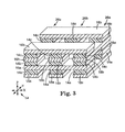
- Figure 3 is a perspective view illustrating one exemplary embodiment of the column line segment stacks.
- Figures 4A and 4B are cross section views illustrating a first embodiment of a memory cell used in a memory storage device according to the present invention.
- Figure 5 is a cross section view illustrating a second embodiment of a memory cell used in a memory storage device according to the present invention.
- Figure 6 is a cross section view illustrating a third embodiment of a memory cell used in a memory storage device according to the present invention.
- Figure 7 is a cross section view illustrating a first exemplary embodiment of the column line segment stacks.
- Figure 8 is a cross section view illustrating a second exemplary embodiment of the column line segment stacks.
- Figure 9 is a top plan view of the second exemplary embodiment illustrated in Figure 8.
- Figure 10 is a layout view of a memory carrier in accordance with the present invention which incorporates the three dimensional memory storage device illustrated and described above.
- Figure 11 is a block diagram of an electronic device in accordance with the present invention which incorporates the three dimensional memory storage device illustrated and described above.
- Figure 12 is a partial perspective view of an embedded memory array in accordance with the present invention which incorporates the three dimensional memory storage device illustrated and described above.
- Figure 1 is a diagram illustrating one exemplary embodiment of a memory storage device 10 according to the present invention.
- an array of column line segment stacks 26 are illustrated which are each intersected by row lines 16.
- row lines 16 each include at least two row lines which are substantially coplanar and parallel and extend in a dimension X, as indicated by arrows 50, to intersect the column line segment stacks 26.
- the row lines 16 can each include any suitable number of individual row lines.
- each base column line 36 is coupled to a corresponding sense amplifier 38 so that the corresponding sense amplifier 38 can read data from memory cells located in the corresponding column line segment stacks 26.
- Each column line segment stack 26 includes at least two memory cells 14. Each of the memory cells 14 are intersected by a unique row line 16 within the row lines 16. The memory cells 14 within each column line segment stack 26 are coupled to either a corresponding line 32 or line 34. Switches 28 and 30 couple, respectively, corresponding conductive pillars or conductive vias 32 or 34 to base column line 36 so that the memory cells 14 within a selected column line segment stack 26 can be read by the corresponding sense amplifier 38. In one embodiment, switches 28 and 30 are implemented with transistors. In one embodiment, the transistors 28/30 are complementary metal oxide semiconductor (CMOS) transistors.
- CMOS complementary metal oxide semiconductor
- FIG. 2 is a schematic diagram illustrating one exemplary embodiment of a memory storage device having memory cells 14 which include a storage element 141 in series with a control element 142.
- each memory cell 14 is coupled to corresponding base column lines 36 and sense amplifiers 38 through a corresponding switch 28 or switch 30.
- switch 28 or switch 30 By selecting either switch 28 or switch 30, the state of each memory cell 14 within a column line segment stack 26 can be read by a corresponding sense amplifier 38.
- memory cells 14 are coupled between a row line 16 and a column line segment 18.
- the row lines 16a and 16b are illustrated at two levels wherein each row line 16 within a particular level are substantially coplanar and parallel and extend in the X dimension, as indicated by arrows 52.
- Row lines 16a are illustrated at a first level which is below the second level of row lines 16b.
- column line segments 18 extend in the Y dimension which is perpendicular to the X dimension as indicated by arrows 52.
- the column line segments 18a and 18b are illustrated at two levels which are between and below row lines 16.
- Each column line segment 18 intersects at least one memory cell 14.
- the column line segments 18b are provided above column line segments 18a and are aligned with column line segments 18a.
- memory cells 14 are provided at three levels which are indicated at 20, 22 and 24 and are defined in a third dimension Z indicated by arrows 52.
- Memory cells 14a illustrated at level 20 are coupled between row lines 16a and column line segments 18a.
- Memory cells 14b illustrated at level 22 are coupled between column line segments 18b and row lines 16a.
- Memory cells 14c illustrated at level 24 are coupled between row lines 16b and column line segments 18b.
- each column line segment 18 and row line 16 intersect a particular memory cell 14.
- memory storage device 10 can be fabricated in other embodiments with any suitable number of levels extending in the Z dimension and with any suitable number of memory cells 14 per layer. In the other embodiments, there can be any suitable number of row lines 16 extending in the X dimension or column line segments 18 extending in the Y dimension.
- each column line segment 18 within a particular column line segment stack 26 is coupled to the corresponding switch 28 or switch 30.
- Adjacent column line segments 18a and 18b are not coupled to the same switch 28 or to the same switch 30 so that memory cells 14 coupled to a particular row line 16 can be individually selected via switch 28 or switch 30.
- each memory cell 14 includes storage element 141 in series with a control element 142.
- the storage element 141 includes an anti-fuse element.
- the control element 142 includes a tunnel junction control element.
- the control element includes a diode.
- storage element 141 is programmed by applying a programming voltage across memory cell 14 to change the resistance of memory cell 14.
- the storage element before being programmed is configured to indicate a first resistance value when a read voltage is applied across storage element 141 and control element 142.
- the storage element 141 after being programmed is configured to indicate a second resistance value when the read voltage is applied across the storage element 141 and control element 142.
- the programming voltage is between one and three volts.
- the read voltage is less than one volt.
- the first resistance value is one megaohm or more.
- the second resistance value is 100 kilohms or less.
- the storage element is configured to be electrically non-conductive before being programmed and is configured to be electrically conductive after being programmed.
- memory cells 14 are formed of an electrically resistive material which is configured to indicate a resistance value when the read voltage is applied across memory cell 14.
- each memory cell 14 includes a resistor in series with the control element.
- the resistance state of a selected memory cell 14 is determined by applying a read voltage across memory cell 14 and measuring the current that flows through memory cell 14.
- a row decoder (not shown) selects a row line 16 by coupling the row line 16 to a voltage potential, hereinafter referred to as V+. All unselected row lines 16 are coupled to a virtual ground voltage, hereinafter referred to as Va.
- the gate of transistor 28 or transistor 30 corresponding to the column line segment 18 and base column line 36 of the selected memory cell 14 have a positive voltage applied to couple the corresponding column line segment 18 to the corresponding base column line 36.
- sense amplifiers 38 hold base column lines 36 at the voltage potential Va. Since the selected memory cell 14 is coupled between the column line segment 18 which is at voltage Va and the selected row line 16 which is at voltage V+, a sense current is conducted through memory cell 14 and the corresponding base conductor line 36 to the corresponding sense amplifier 38.
- the sense amplifier 38 is configured to provide the state of the selected memory cell 14 based on the conducted current.
- the unselected row lines 16 and the selected base column line 36 and column line segment 18 are held at the voltage Va during the read operation to limit unintended leakage currents from being coupled to the sense amplifiers 38 during the read operation.
- the number of column line segments 18 within a particular column line segment stack 26, as well as the number of memory cells 14 coupled to the particular column line segment 18, are optimized to limit the leakage currents coupled to sense amplifier 38 during the read operation.
- Figure 3 is a perspective view illustrating one exemplary embodiment of the column line segment stacks 26.
- Figure 3 illustrates three column line segment stacks at 26a, 26b and 26c.
- Row lines 16a and 16b each are an array of conductors formed of a conductive material which intersects either a top side or a bottom side of memory cells 14.
- Column line segments 18a and 18b each are an array of conductors and are formed of a conductive material which intersects either a top side or a bottom side of memory cells 14.
- Figure 3 illustrates that each memory cell 14 is intersected by one row line 16 and one column line segment 18. In other embodiments, other suitable arrangements of column line segments 18 and row lines 16 with corresponding memory cells 14 may be used within the scope of the present invention.
- Figures 4A and 4B are cross section views illustrating a first embodiment of a memory cell 14 used in a memory storage device according to the present invention.
- Figures 4A and 4B illustrate that each memory cell 14 is intersected and electrically coupled to a row line 16 and a column line segment 18.
- Memory cells in various embodiments are electrically coupled at a top side to column line segment 18 and at a bottom side to row lines 16, or at a bottom side to column line segments 18 and at a top side to row lines 16.
- Figure 4A illustrates a tunnel junction storage element 141 electrically coupled via electrode 41 to a tunnel junction control element 142.
- Control element 142 is electrically coupled to column line segments 18 via electrode 42.
- Storage element 141 is electrically coupled to row line 16 via electrode 40.
- Electrodes 40, 41 and 42 provide a low resistance contact to control element 142 and storage element 141 to minimize any unintended resistance to current flow through memory cell 14. In other embodiments, electrodes 40, 41 or 42 are not used.
- Figure 4B illustrates a cross section of Figure 4A along lines 4B-4B to illustrate that row line 16 extends in a first dimension and column line segment 18 extends in a second dimension, wherein the first dimension and the second dimension in the illustrated embodiment are perpendicular. In other embodiments, row lines 16 and column line segments 18 are not perpendicular. In various embodiments, the process illustrated in Figure 4 is repeated to stack multiple layers to form the column line segment stacks 26.
- Figure 5 is a cross section view illustrating a second embodiment of a memory cell 14 used in a memory storage device according to the present invention.
- a row line 16 is formed of a conductive thin-film such as aluminum and is deposited and etched to define row line 16.
- a planar dielectric layer 62 is formed over and above row line 16.
- oxide portion 60 is formed through self-oxidation, is thermally grown, or is deposited. In one embodiment, oxide portion 60 has a thickness which is less than 100 Angstroms. In other embodiments, oxide portion 60 has a thickness which is less than 50 Angstroms.
- a conductive thin-film metal layer 66 is deposited over dielectric layer 62 and a dielectric layer is completed to fill the open etched via region 64.
- a CMP step is completed to remove portions of metal layer 66 to define an exposed edge 68.
- An oxide layer 72 which includes a portion 70 overlying the exposed edge 68 is next formed over the planarized surface.
- a conductive thin-film is deposited and etched to define column line segment 18 and a dielectric filler layer 74 is formed over and above column line 18.
- the process illustrated in Figure 5 is repeated to stack multiple layers to form the column line segment stacks 26.
- row line 16 and column line segment 18 are formed of aluminum, copper, silicide or alloys, or other suitable conductive metals or semiconductor materials.
- oxide layer 72 is formed of any suitable electrically insulative material which includes, but is not limited to, oxide-nitride-oxide (ONO), tantalum pentoxide (Ta 2 O 5 ), plasma enhanced silicon nitride (P-SiN x ), titanium oxide, germanium oxide, any chemical vapor deposition (CVD) dielectric including a deposited oxide, a grown oxide, or any other suitable dielectric material.
- dielectric layer 62 and dielectric layer 74 are formed of suitable electrically insulative materials which include, but are not limited to, a wet or dry silicon dioxide (SiO 2 ), a nitride material including silicon nitride, tetraethylorthosilicate (Si-OC 2 H 5 ), TEOS based oxides including oxides formed by a deposition resulting from the decomposition of a TEOS gas in a reactor, borophosphosilicate glass (BPSG), phosphosilicate glass (PSG), borosilicate glass (BSG), polyamide film, oxynitride, spin on glass (SOG), any chemical vapor deposited (CVD) dielectric including a deposited oxide or a grown oxide, any physical vapor deposition (PVD) dielectric, or a sputtered dielectric.
- suitable electrically insulative materials which include, but are not limited to, a wet or dry silicon dioxide (SiO 2 ), a nitrid
- row line 16, oxide portion 60 and metal layer 66 form the control element 142.
- metal layer 66, oxide portion 70 and column line segment 18 form the storage element 141.
- Storage element 141 utilizes electron tunneling to create the storage structure.
- the electron tunneling can be direct tunneling thereby requiring a minimal oxide layer thickness.
- the oxide layer thickness is within a range of approximately 5 to 50 Angstroms. In other embodiments, other suitable oxide layer thicknesses can be used.
- storage element 141 is an anti-fuse element. In other embodiments, storage element 141 utilizes mechanisms such as dielectric rupture dynamics to create the storage structure.
- the current through oxide portion 70 can be in the low microampere or nanoampere range, thereby resulting in low power dissipation.
- the current can be in the high nanoampere to microamp range. This difference in current levels creates a very good signal to noise ratio for sensing whether the oxide portion 70 is programmed to have a logical "0" or a logical "1" state. While the illustrated current ranges are approximate current ranges for 0.18 micron process geometries, the actual current ranges can vary in accordance with the actual process geometries used.
- the oxide portion 70 can have higher current flow as a result of tunneling current.
- the tunneling current creates a flow of electrons that locally heat storage element 141, thereby forming conductive filaments through oxide portion 70.
- the conductive filaments are formed when sufficient energy is forced across the oxide portion 70 barrier to heat the fusing site, resulting in the state of the oxide portion 70 being changed permanently.
- the oxide portion 70 can be processed to be a dielectric breakdown device rather than a tunnel junction device.
- Figure 6 is a cross section view illustrating a third embodiment of a memory cell 14 used in a memory storage device according to the present invention.
- the construction of memory cell 14 is similar to the embodiment of Figure 5 with the exception that the illustration in Figure 6 includes a state-change layer 76.
- phase-change materials can be used for a read/writeable (or write/erase/write) state-change layer in accordance with the present invention.
- germanium telluride (GeTe) is used. GeTe can be reversibly changed from a semiconducting (amorphous) state to a metallic (crystalline) state by undergoing heating and cooling steps at a suitable rate.
- the GeTe is doped so that it is p-type when in its semiconducting state.
- GeTe is deposited over an n-type semiconductor layer, a large contrast is observed in the number of carriers swept across the junction when compared to GeTe in the metallic state.
- the memory cell is read-writeable or capable of being written, erased, and written.
- phase-change materials can be used which include, but are not limited to, chalcogenide alloys such as GaSb, InSb, InSe, Sb 2 Te 3 , Ge 2 Sb 2 Te 5 , InSbTe, GaSeTe, SnSb 2 Te 4 , InSbGe, AglnSbTe, (GeSn)SbTe, GeSb(SeTe), Te 81 Ge 15 Sb 2 S 2 and GeSbTe.
- chalcogenide alloys such as GaSb, InSb, InSe, Sb 2 Te 3 , Ge 2 Sb 2 Te 5 , InSbTe, GaSeTe, SnSb 2 Te 4 , InSbGe, AglnSbTe, (GeSn)SbTe, GeSb(SeTe), Te 81 Ge 15 Sb 2 S 2 and GeSbTe.
- alternative state-change technologies can be used to construct memory cell 14. These technologies include, but are not limited to, a LeComber switch or a silicide switch.
- the LeComber switch is formed by depositing a thin layer of amorphous intrinsic silicon over a metallic conductor such as row line 16 or column line segment 18.
- the conductor can be formed by a number of suitable materials which include Chromium (Cr).
- Cr Chromium
- Au gold
- the LeComber switch performs as a reversed biased tunnel diode before being programmed.
- the LeComber switch is programmed by creating an enhanced concentrated electric field through the amorphous silicon to form a conductive path.
- the silicide switch is formed by stacking alternating silicon and transition metal thin films so that the alternating films exhibit a changed resistance when programmed.
- the programming process for a silicide switch is irreversible.
- the stacked silicon and transaction metal layers have a first resistance.
- Appropriate row and column lines are selected to force a current through a selected memory cell.
- the current passing through the selected memory cell creates Joule heat which triggers and completes the silicidation reaction.
- the silicidation reaction causes the resistance of the selected memory cell to change to a lower value.
- a small sense current is supplied to the memory cell and the voltage drop across the memory cell is measured.
- silicide compounds can be used which include, but are not limited to, Ni 2 Si, NiSi, NiSi 2 , Pd2Si, PdSi, and Pt 2 Si, and PtSi.
- other transition metals in various compounds with silicon can be used which include, but are not limited to, Ti, V, Cr, Mn, Fe, Co, Zr, Nb, Mo, Rh, Hf, Ta, W, and Ir.
- the process illustrated in Figure 6 is repeated to stack multiple layers to form the column line segment stacks 26.
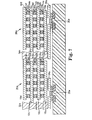
- Figure 7 is a cross section view illustrating a first exemplary embodiment of a column line segment stack 26.
- Figure 7 illustrates two column line segment stacks 26a corresponding to a base conductor line illustrated at 36a.
- Row lines 16 extend in a first dimension and are illustrated at 16a through 16c.
- Column line segments 18 extend in a second dimension and are illustrated at 18a through 18d.
- Memory cell arrays 14a through 14f intersect column line segments 18a through 18d such that each column line segment 18 intersects at least one memory cell 14.
- Each memory cell 14 is intersected by a unique row line 16.
- conductive pillars or conductive vias 32a and 34a are coupled to column line segments 18 so that each column line segment 18 intersects memory cells 14 which do not intersect the same row line 16.
- the interconnection arrangement of row lines 16, column line segments 18 and memory cells 14 allow each memory cell 14 to be intersected by a unique row line 16 and column line segment 18 and be selected through the corresponding select switch 28a or select switch 30a.
- Figure 8 is a cross section view illustrating a second exemplary embodiment of a column line segment stack 26.
- Figure 8 illustrates an interconnection arrangement for column line segment stacks 26a which is similar to the embodiment of Figure 7 with the difference being that each column line segment 18 intersects three memory cells 14, wherein in the embodiment illustrated in Figure 7, each column line segment 18 intersects six memory cells 14.
- select switches 28a or 30a are coupled through select switches 28a or 30a to sense amplifiers 38 during the read operation, because each column line segment 18 intersects three rather than the six memory cells 14 illustrated in Figure 7.
- other suitable numbers of column line segments 18 may be used.
- FIGS 7 and 8 illustrate respectively six memory cells 14 and three memory cells 14 intersecting a single column line segment 18 in other embodiments, other suitable numbers of memory cells can intersect each column line segment 18, depending on the level of leakage currents which can be tolerated.
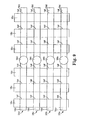
- Figure 9 is a top plan view of the second exemplary embodiment illustrated in Figure 8.
- Figure 9 illustrates column line segment stacks 26a through 26d wherein conductive pillars or conductive vias 34 couple column line segments 18 to adjacent column line segments 18 between column line segment stacks 26.
- Each column line segment stack 26 includes three row conductors 16c which are perpendicular to the column line segments 18d.
- Column line segments 18d are aligned with corresponding column line segments 18a through 18c.
- Each memory cell 14f is intersected by a row line 16 and a column line segment 18.
- FIG 10 is a layout view of a memory carrier 80 in accordance with the present invention which incorporates the three dimensional memory storage device illustrated and described above.
- memory carrier 80 includes one or more memory storage devices 82.
- memory carrier 80 can use any suitable memory card format which includes, but is not limited to, PCMCIA, PC card, smart memory, secure digital (SD), multi-media card (MMC), memory stick, digital film, ATA, and compact flash.
- memory carrier 80 includes a mechanical interface 84 that provides for both mechanical and electrical contact with a connector suitable for memory carrier 80.
- an electrical interface 86 electrically couples with electrical contacts on mechanical interface 84 and provides suitable functions which include security, address decoding, voltage translation or write protection for memory storage devices 82.
- memory carrier 80 can be a printed circuit board or ceramic substrate which physically supports memory storage devices 82, electrical interface 86 and mechanical interface 84.
- FIG 11 is a block diagram of an electronic device in accordance with the present invention which incorporates the three dimensional memory storage device illustrated and described above.
- the electronic device is a computer system 90.
- a microprocessor 92 is coupled to a memory storage device 94.
- memory storage device 94 is used to hold computer executable instructions and/or user data.
- Other applications for memory storage device 94 can include BIOS memory, DRAM memory, ROM, or various levels of internal or external cache memory.
- microprocessor 92 is connected to a storage device 96 which can be a hard disk drive, floppy drive, CD/DVD drive, tape drive or other suitable mass storage device.
- Both microprocessor 92 and memory circuit 94 can include one or more memory storage devices according to the present invention.
- microprocessor 92 is connected to a display device 98 that can include memory storage devices according to the present invention.
- the memory storage device of the present invention can be included within many memory storage application areas within computer system 90.
- FIG 12 is a partial perspective view of an embedded memory array 100 in accordance with the present invention which incorporates the three dimensional memory storage device illustrated and described above.
- embedded memory array 100 is fabricated on top of a microprocessor 104 to minimize the die area size.
- Microprocessor 104 forms a horizontal substrate surface.
- memory array 100 is built of one or more vertical layers 102 of memory cells 14 to form the embedded memory array 100.
- Microprocessor 102 is electrically attached to a package 106 via bonding wires 108.
- other suitable packaging technologies such as Tape Automated Bonding (TAB) can be used.
- TAB Tape Automated Bonding
Landscapes
- Engineering & Computer Science (AREA)
- Microelectronics & Electronic Packaging (AREA)
- Semiconductor Memories (AREA)
Abstract
Description
- The present invention relates to the field of integrated circuit memories. More particularly the present invention relates to a memory storage device and method for a three dimensional cross point memory array.
- As the demand for integrated circuits continues to rise, manufacturers labor to incorporate increasingly greater numbers of transistors onto each die. Integrated circuit memories often times have higher transistor densities than other types of circuits, and as a result, tend to push the leading edge of the technology envelope. The memories are typically organized into two dimensional arrays wherein each memory cell in the array is intersected by a row conductor and a column conductor. The two dimensional memory arrays are often times limited in memory cell density by the minimum line widths of the technology used to fabricate the array. As a result, improvements in the memory densities are achieved when the minimum feature sizes of the integrated circuit process used to fabricate the memories are decreased.
- One popular type of memory is a read-only memory (ROM). The two most common types of ROMs are mask ROMs and field programmable ROMs. With mask ROMs, the information stored in each memory cell is permanently programmed during the fabrication process and cannot be subsequently changed. Field programmable ROMs are not programmed during the fabrication process and are more desirable because they enable end users to store a single part type which can be used in many applications.
- One type of field programmable ROM includes memory cells which have a storage element and a control component. The storage elements typically have a high resistance to current flow and can be programmed to have a low resistance by application of a suitable voltage across the storage element. The programmed configuration can be sensed by application of a read voltage across the storage element and by comparing the current passed through the programmed storage element to the current passed through a non-programmed storage element.
- One disadvantage of the two dimensional ROM arrays are leakage currents which tend to make accurate memory reads more difficult as the number of memory cells in the arrays are increased. For example, the row and column lines which intersect memory cells in the array travel the entire length of the array. If a particular row and column line are selected and the read voltage is applied, other storage elements positioned along the row line or along the column line can provide leakage currents which make it more difficult to detect the difference between the non-programmed and programmed configurations. One approach to limit the leakage currents is to separate the column lines into portions which are each separately addressable. To accomplish this, additional peripheral circuitry must be added to read and write the individual column line portions. While this approach can reduce leakage currents by reducing the number of unselected storage elements connected to each column line portion, the number of memory cells in the array must be decreased to make room for the additional read and write circuits.
- In view of the above, there is a need for an improved memory which has greater memory cell densities and reduced leakage currents.
- One aspect of the present invention provides a memory storage device and method. The memory storage device includes a first and second memory cell which each have a top end and a bottom end. A first and second first dimension conductor are substantially coplanar and parallel and extend in a first dimension. The first first dimension conductor intersects the bottom end of the first memory cell and the second first dimension conductor intersects the top end of the second memory cell. A first second dimension conductor extends in a second dimension and intersects the top end of the first memory cell and a second second dimension conductor extends in the second dimension and intersects the bottom end of the second memory cell. A first third dimension conductor extends in a third dimension and is positioned between the first and second memory cell to couple the first second dimension conductor to the second second dimension conductor.
- Figure 1 is a diagram illustrating one exemplary embodiment of a memory storage device according to the present invention.
- Figure 2 is a schematic diagram illustrating one exemplary embodiment of a memory storage device having memory cells which include a storage element in series with a control element.
- Figure 3 is a perspective view illustrating one exemplary embodiment of the column line segment stacks.
- Figures 4A and 4B are cross section views illustrating a first embodiment of a memory cell used in a memory storage device according to the present invention.
- Figure 5 is a cross section view illustrating a second embodiment of a memory cell used in a memory storage device according to the present invention.
- Figure 6 is a cross section view illustrating a third embodiment of a memory cell used in a memory storage device according to the present invention.
- Figure 7 is a cross section view illustrating a first exemplary embodiment of the column line segment stacks.
- Figure 8 is a cross section view illustrating a second exemplary embodiment of the column line segment stacks.
- Figure 9 is a top plan view of the second exemplary embodiment illustrated in Figure 8.
- Figure 10 is a layout view of a memory carrier in accordance with the present invention which incorporates the three dimensional memory storage device illustrated and described above.
- Figure 11 is a block diagram of an electronic device in accordance with the present invention which incorporates the three dimensional memory storage device illustrated and described above.
- Figure 12 is a partial perspective view of an embedded memory array in accordance with the present invention which incorporates the three dimensional memory storage device illustrated and described above.
- In the following detailed description of the preferred embodiments, reference is made to the accompanying drawings which form a part hereof, and in which is shown by way of illustration specific embodiments in which the invention may be practiced. It is to be understood that other embodiments may be utilized and structural or logical changes may be made without departing from the scope of the present invention. The following detailed description, therefore, is not to be taken in a limiting sense, and the scope of the present invention is defined by the appended claims.
- Figure 1 is a diagram illustrating one exemplary embodiment of a
memory storage device 10 according to the present invention. In the illustrated embodiment, an array of column line segment stacks 26 are illustrated which are each intersected byrow lines 16. In the illustrated embodiment,row lines 16 each include at least two row lines which are substantially coplanar and parallel and extend in a dimension X, as indicated byarrows 50, to intersect the column line segment stacks 26. In other embodiments, therow lines 16 can each include any suitable number of individual row lines. - In the illustrated embodiment, three base column lines which extend in a dimension Y, perpendicular to the X dimension as indicated by
arrows 50, are illustrated at 36a, 36b, and 36c. In other embodiments, there can be any suitable number of base column lines 36. Each base column line 36 is coupled to a corresponding sense amplifier 38 so that the corresponding sense amplifier 38 can read data from memory cells located in the corresponding column line segment stacks 26. - Each column line segment stack 26 includes at least two
memory cells 14. Each of thememory cells 14 are intersected by aunique row line 16 within therow lines 16. Thememory cells 14 within each column line segment stack 26 are coupled to either a corresponding line 32 or line 34. Switches 28 and 30 couple, respectively, corresponding conductive pillars or conductive vias 32 or 34 to base column line 36 so that thememory cells 14 within a selected column line segment stack 26 can be read by the corresponding sense amplifier 38. In one embodiment, switches 28 and 30 are implemented with transistors. In one embodiment, the transistors 28/30 are complementary metal oxide semiconductor (CMOS) transistors. - Figure 2 is a schematic diagram illustrating one exemplary embodiment of a memory storage device having
memory cells 14 which include astorage element 141 in series with acontrol element 142. In the illustrated embodiment, eachmemory cell 14 is coupled to corresponding base column lines 36 and sense amplifiers 38 through a corresponding switch 28 or switch 30. By selecting either switch 28 or switch 30, the state of eachmemory cell 14 within a column line segment stack 26 can be read by a corresponding sense amplifier 38. - In the illustrated embodiment,
memory cells 14 are coupled between arow line 16 and acolumn line segment 18. The row lines 16a and 16b are illustrated at two levels wherein eachrow line 16 within a particular level are substantially coplanar and parallel and extend in the X dimension, as indicated byarrows 52.Row lines 16a are illustrated at a first level which is below the second level ofrow lines 16b. In the illustrated embodiment,column line segments 18 extend in the Y dimension which is perpendicular to the X dimension as indicated byarrows 52. Thecolumn line segments column line segment 18 intersects at least onememory cell 14. Thecolumn line segments 18b are provided abovecolumn line segments 18a and are aligned withcolumn line segments 18a. - In the illustrated embodiment,
memory cells 14 are provided at three levels which are indicated at 20, 22 and 24 and are defined in a third dimension Z indicated byarrows 52.Memory cells 14a illustrated atlevel 20 are coupled betweenrow lines 16a andcolumn line segments 18a.Memory cells 14b illustrated atlevel 22 are coupled betweencolumn line segments 18b androw lines 16a.Memory cells 14c illustrated atlevel 24 are coupled betweenrow lines 16b andcolumn line segments 18b. In the illustrated embodiment, eachcolumn line segment 18 androw line 16 intersect aparticular memory cell 14. - The illustrated embodiment is abbreviated to better illustrate the scope of the present invention. Those skilled in the art will appreciate that
memory storage device 10 can be fabricated in other embodiments with any suitable number of levels extending in the Z dimension and with any suitable number ofmemory cells 14 per layer. In the other embodiments, there can be any suitable number ofrow lines 16 extending in the X dimension orcolumn line segments 18 extending in the Y dimension. - In the illustrated embodiment, each
column line segment 18 within a particular column line segment stack 26 is coupled to the corresponding switch 28 or switch 30. Adjacentcolumn line segments memory cells 14 coupled to aparticular row line 16 can be individually selected via switch 28 or switch 30. - In the illustrated embodiment, each
memory cell 14 includesstorage element 141 in series with acontrol element 142. In one embodiment, thestorage element 141 includes an anti-fuse element. In one embodiment, thecontrol element 142 includes a tunnel junction control element. In one embodiment, the control element includes a diode. - In the illustrated embodiment,
storage element 141 is programmed by applying a programming voltage acrossmemory cell 14 to change the resistance ofmemory cell 14. In one embodiment, the storage element before being programmed is configured to indicate a first resistance value when a read voltage is applied acrossstorage element 141 andcontrol element 142. Thestorage element 141 after being programmed is configured to indicate a second resistance value when the read voltage is applied across thestorage element 141 andcontrol element 142. In one embodiment, the programming voltage is between one and three volts. In one embodiment, the read voltage is less than one volt. In one embodiment, the first resistance value is one megaohm or more. In one embodiment, the second resistance value is 100 kilohms or less. In one embodiment, the storage element is configured to be electrically non-conductive before being programmed and is configured to be electrically conductive after being programmed. In one embodiment,memory cells 14 are formed of an electrically resistive material which is configured to indicate a resistance value when the read voltage is applied acrossmemory cell 14. In other embodiments, eachmemory cell 14 includes a resistor in series with the control element. - In the illustrated embodiment, the resistance state of a selected
memory cell 14 is determined by applying a read voltage acrossmemory cell 14 and measuring the current that flows throughmemory cell 14. During a read operation to determine the state or resistance value of a selectedmemory cell 14, a row decoder (not shown) selects arow line 16 by coupling therow line 16 to a voltage potential, hereinafter referred to as V+. Allunselected row lines 16 are coupled to a virtual ground voltage, hereinafter referred to as Va. The gate of transistor 28 or transistor 30 corresponding to thecolumn line segment 18 and base column line 36 of the selectedmemory cell 14 have a positive voltage applied to couple the correspondingcolumn line segment 18 to the corresponding base column line 36. During the read operation, sense amplifiers 38 hold base column lines 36 at the voltage potential Va. Since the selectedmemory cell 14 is coupled between thecolumn line segment 18 which is at voltage Va and the selectedrow line 16 which is at voltage V+, a sense current is conducted throughmemory cell 14 and the corresponding base conductor line 36 to the corresponding sense amplifier 38. The sense amplifier 38 is configured to provide the state of the selectedmemory cell 14 based on the conducted current. - In the illustrated embodiment, the
unselected row lines 16 and the selected base column line 36 andcolumn line segment 18 are held at the voltage Va during the read operation to limit unintended leakage currents from being coupled to the sense amplifiers 38 during the read operation. In various embodiments, the number ofcolumn line segments 18 within a particular column line segment stack 26, as well as the number ofmemory cells 14 coupled to the particularcolumn line segment 18, are optimized to limit the leakage currents coupled to sense amplifier 38 during the read operation. - Figure 3 is a perspective view illustrating one exemplary embodiment of the column line segment stacks 26. Figure 3 illustrates three column line segment stacks at 26a, 26b and 26c.
Row lines memory cells 14.Column line segments memory cells 14. Figure 3 illustrates that eachmemory cell 14 is intersected by onerow line 16 and onecolumn line segment 18. In other embodiments, other suitable arrangements ofcolumn line segments 18 androw lines 16 withcorresponding memory cells 14 may be used within the scope of the present invention. - Figures 4A and 4B are cross section views illustrating a first embodiment of a
memory cell 14 used in a memory storage device according to the present invention. Figures 4A and 4B illustrate that eachmemory cell 14 is intersected and electrically coupled to arow line 16 and acolumn line segment 18. Memory cells in various embodiments are electrically coupled at a top side tocolumn line segment 18 and at a bottom side to rowlines 16, or at a bottom side tocolumn line segments 18 and at a top side to rowlines 16. - Figure 4A illustrates a tunnel
junction storage element 141 electrically coupled viaelectrode 41 to a tunneljunction control element 142.Control element 142 is electrically coupled tocolumn line segments 18 viaelectrode 42.Storage element 141 is electrically coupled to rowline 16 viaelectrode 40.Electrodes element 142 andstorage element 141 to minimize any unintended resistance to current flow throughmemory cell 14. In other embodiments,electrodes - Figure 4B illustrates a cross section of Figure 4A along
lines 4B-4B to illustrate thatrow line 16 extends in a first dimension andcolumn line segment 18 extends in a second dimension, wherein the first dimension and the second dimension in the illustrated embodiment are perpendicular. In other embodiments,row lines 16 andcolumn line segments 18 are not perpendicular. In various embodiments, the process illustrated in Figure 4 is repeated to stack multiple layers to form the column line segment stacks 26. - Figure 5 is a cross section view illustrating a second embodiment of a
memory cell 14 used in a memory storage device according to the present invention. In the illustrated embodiment, arow line 16 is formed of a conductive thin-film such as aluminum and is deposited and etched to definerow line 16. Aplanar dielectric layer 62 is formed over and aboverow line 16. - In the illustrated embodiment, after
dielectric layer 62 has been formed, an etch step is completed to define an etched viaregion 64. The exposedrow line 16 in the bottom of viaregion 64 is oxidized to form anoxide portion 60. In various embodiments,oxide portion 60 is formed through self-oxidation, is thermally grown, or is deposited. In one embodiment,oxide portion 60 has a thickness which is less than 100 Angstroms. In other embodiments,oxide portion 60 has a thickness which is less than 50 Angstroms. Afteroxide portion 60 is formed, a conductive thin-film metal layer 66 is deposited overdielectric layer 62 and a dielectric layer is completed to fill the open etched viaregion 64. A CMP step is completed to remove portions ofmetal layer 66 to define an exposededge 68. Anoxide layer 72 which includes aportion 70 overlying the exposededge 68 is next formed over the planarized surface. A conductive thin-film is deposited and etched to definecolumn line segment 18 and adielectric filler layer 74 is formed over and abovecolumn line 18. In various embodiments, the process illustrated in Figure 5 is repeated to stack multiple layers to form the column line segment stacks 26. - In various embodiments,
row line 16 andcolumn line segment 18 are formed of aluminum, copper, silicide or alloys, or other suitable conductive metals or semiconductor materials. In various embodiments,oxide layer 72 is formed of any suitable electrically insulative material which includes, but is not limited to, oxide-nitride-oxide (ONO), tantalum pentoxide (Ta2O5), plasma enhanced silicon nitride (P-SiNx), titanium oxide, germanium oxide, any chemical vapor deposition (CVD) dielectric including a deposited oxide, a grown oxide, or any other suitable dielectric material. In various embodiments,dielectric layer 62 anddielectric layer 74 are formed of suitable electrically insulative materials which include, but are not limited to, a wet or dry silicon dioxide (SiO2), a nitride material including silicon nitride, tetraethylorthosilicate (Si-OC2H5), TEOS based oxides including oxides formed by a deposition resulting from the decomposition of a TEOS gas in a reactor, borophosphosilicate glass (BPSG), phosphosilicate glass (PSG), borosilicate glass (BSG), polyamide film, oxynitride, spin on glass (SOG), any chemical vapor deposited (CVD) dielectric including a deposited oxide or a grown oxide, any physical vapor deposition (PVD) dielectric, or a sputtered dielectric. - In the illustrated embodiment,
row line 16,oxide portion 60 andmetal layer 66 form thecontrol element 142. In the illustrated embodiment,metal layer 66,oxide portion 70 andcolumn line segment 18 form thestorage element 141.Storage element 141 utilizes electron tunneling to create the storage structure. In the illustrated embodiment, the electron tunneling can be direct tunneling thereby requiring a minimal oxide layer thickness. In various embodiments, the oxide layer thickness is within a range of approximately 5 to 50 Angstroms. In other embodiments, other suitable oxide layer thicknesses can be used. In one embodiment,storage element 141 is an anti-fuse element. In other embodiments,storage element 141 utilizes mechanisms such as dielectric rupture dynamics to create the storage structure. - In various embodiments, when a low voltage potential is present across
oxide portion 70 such as when reading the memory cell, the current throughoxide portion 70 can be in the low microampere or nanoampere range, thereby resulting in low power dissipation. Whenstorage element 141 is programmed by creating filaments throughoxide portion 70, the current can be in the high nanoampere to microamp range. This difference in current levels creates a very good signal to noise ratio for sensing whether theoxide portion 70 is programmed to have a logical "0" or a logical "1" state. While the illustrated current ranges are approximate current ranges for 0.18 micron process geometries, the actual current ranges can vary in accordance with the actual process geometries used. - In various embodiments, at higher voltage potentials, such as when programming
storage element 141, theoxide portion 70 can have higher current flow as a result of tunneling current. The tunneling current creates a flow of electrons that locallyheat storage element 141, thereby forming conductive filaments throughoxide portion 70. The conductive filaments are formed when sufficient energy is forced across theoxide portion 70 barrier to heat the fusing site, resulting in the state of theoxide portion 70 being changed permanently. In other embodiments, theoxide portion 70 can be processed to be a dielectric breakdown device rather than a tunnel junction device. - Figure 6 is a cross section view illustrating a third embodiment of a
memory cell 14 used in a memory storage device according to the present invention. The construction ofmemory cell 14 is similar to the embodiment of Figure 5 with the exception that the illustration in Figure 6 includes a state-change layer 76. Many suitable phase-change materials can be used for a read/writeable (or write/erase/write) state-change layer in accordance with the present invention. In one embodiment, germanium telluride (GeTe) is used. GeTe can be reversibly changed from a semiconducting (amorphous) state to a metallic (crystalline) state by undergoing heating and cooling steps at a suitable rate. In one embodiment, the GeTe is doped so that it is p-type when in its semiconducting state. When GeTe is deposited over an n-type semiconductor layer, a large contrast is observed in the number of carriers swept across the junction when compared to GeTe in the metallic state. In various embodiments, when using GeTe or other suitable phase-change materials, the memory cell is read-writeable or capable of being written, erased, and written. In other embodiments, other phase-change materials can be used which include, but are not limited to, chalcogenide alloys such as GaSb, InSb, InSe, Sb2Te3, Ge2Sb2Te5, InSbTe, GaSeTe, SnSb2Te4 , InSbGe, AglnSbTe, (GeSn)SbTe, GeSb(SeTe), Te81Ge15Sb2S2 and GeSbTe. - In other embodiments, alternative state-change technologies can be used to construct
memory cell 14. These technologies include, but are not limited to, a LeComber switch or a silicide switch. The LeComber switch is formed by depositing a thin layer of amorphous intrinsic silicon over a metallic conductor such asrow line 16 orcolumn line segment 18. The conductor can be formed by a number of suitable materials which include Chromium (Cr). After the thin layer of amorphous intrinsic silicon is deposited, a separate metal such as gold (Ag) is deposited over the layer of amorphous intrinsic silicon. The LeComber switch performs as a reversed biased tunnel diode before being programmed. The LeComber switch is programmed by creating an enhanced concentrated electric field through the amorphous silicon to form a conductive path. - The silicide switch is formed by stacking alternating silicon and transition metal thin films so that the alternating films exhibit a changed resistance when programmed. Generally, the programming process for a silicide switch is irreversible. Before writing, the stacked silicon and transaction metal layers have a first resistance. Appropriate row and column lines are selected to force a current through a selected memory cell. The current passing through the selected memory cell creates Joule heat which triggers and completes the silicidation reaction. By applying a concentrated electric field, the current is focused and the Joule heat is concentrated in a small area which allows the programming to be completed. The silicidation reaction causes the resistance of the selected memory cell to change to a lower value. To read the programmed memory cell, a small sense current is supplied to the memory cell and the voltage drop across the memory cell is measured. In various embodiments, many suitable silicide compounds can be used which include, but are not limited to, Ni2Si, NiSi, NiSi2, Pd2Si, PdSi, and Pt2Si, and PtSi. In other embodiments, other transition metals in various compounds with silicon can be used which include, but are not limited to, Ti, V, Cr, Mn, Fe, Co, Zr, Nb, Mo, Rh, Hf, Ta, W, and Ir. In various embodiments, the process illustrated in Figure 6 is repeated to stack multiple layers to form the column line segment stacks 26.
- Figure 7 is a cross section view illustrating a first exemplary embodiment of a column line segment stack 26. Figure 7 illustrates two column
line segment stacks 26a corresponding to a base conductor line illustrated at 36a. Rowlines 16 extend in a first dimension and are illustrated at 16a through 16c.Column line segments 18 extend in a second dimension and are illustrated at 18a through 18d.Memory cell arrays 14a through 14f intersectcolumn line segments 18a through 18d such that eachcolumn line segment 18 intersects at least onememory cell 14. Eachmemory cell 14 is intersected by aunique row line 16. In the illustrated embodiment, conductive pillars orconductive vias column line segments 18 so that eachcolumn line segment 18 intersectsmemory cells 14 which do not intersect thesame row line 16. The interconnection arrangement ofrow lines 16,column line segments 18 andmemory cells 14 allow eachmemory cell 14 to be intersected by aunique row line 16 andcolumn line segment 18 and be selected through the correspondingselect switch 28a orselect switch 30a. - Figure 8 is a cross section view illustrating a second exemplary embodiment of a column line segment stack 26. Figure 8 illustrates an interconnection arrangement for column
line segment stacks 26a which is similar to the embodiment of Figure 7 with the difference being that eachcolumn line segment 18 intersects threememory cells 14, wherein in the embodiment illustrated in Figure 7, eachcolumn line segment 18 intersects sixmemory cells 14. In the embodiment illustrated in Figure 8, smaller amounts of unintended leakage currents are coupled throughselect switches column line segment 18 intersects three rather than the sixmemory cells 14 illustrated in Figure 7. In other embodiments, other suitable numbers ofcolumn line segments 18 may be used. While the embodiments illustrated in Figures 7 and 8 illustrate respectively sixmemory cells 14 and threememory cells 14 intersecting a singlecolumn line segment 18 in other embodiments, other suitable numbers of memory cells can intersect eachcolumn line segment 18, depending on the level of leakage currents which can be tolerated. - Figure 9 is a top plan view of the second exemplary embodiment illustrated in Figure 8. Figure 9 illustrates column
line segment stacks 26a through 26d wherein conductive pillars or conductive vias 34 couplecolumn line segments 18 to adjacentcolumn line segments 18 between column line segment stacks 26. Each column line segment stack 26 includes threerow conductors 16c which are perpendicular to thecolumn line segments 18d.Column line segments 18d are aligned with correspondingcolumn line segments 18a through 18c. Eachmemory cell 14f is intersected by arow line 16 and acolumn line segment 18. - Figure 10 is a layout view of a
memory carrier 80 in accordance with the present invention which incorporates the three dimensional memory storage device illustrated and described above. In the illustrated embodiment,memory carrier 80 includes one or morememory storage devices 82. In various embodiments,memory carrier 80 can use any suitable memory card format which includes, but is not limited to, PCMCIA, PC card, smart memory, secure digital (SD), multi-media card (MMC), memory stick, digital film, ATA, and compact flash. In the illustrated embodiment,memory carrier 80 includes amechanical interface 84 that provides for both mechanical and electrical contact with a connector suitable formemory carrier 80. In another embodiment, anelectrical interface 86 electrically couples with electrical contacts onmechanical interface 84 and provides suitable functions which include security, address decoding, voltage translation or write protection formemory storage devices 82. In various embodiments,memory carrier 80 can be a printed circuit board or ceramic substrate which physically supportsmemory storage devices 82,electrical interface 86 andmechanical interface 84. - Figure 11 is a block diagram of an electronic device in accordance with the present invention which incorporates the three dimensional memory storage device illustrated and described above. In the embodiment illustrated in Figure 11, the electronic device is a
computer system 90. In the illustrated embodiment, amicroprocessor 92 is coupled to amemory storage device 94. In various embodiments,memory storage device 94 is used to hold computer executable instructions and/or user data. Other applications formemory storage device 94 can include BIOS memory, DRAM memory, ROM, or various levels of internal or external cache memory. In the illustrated embodiment,microprocessor 92 is connected to astorage device 96 which can be a hard disk drive, floppy drive, CD/DVD drive, tape drive or other suitable mass storage device. Bothmicroprocessor 92 andmemory circuit 94 can include one or more memory storage devices according to the present invention. In the illustrated embodiment,microprocessor 92 is connected to adisplay device 98 that can include memory storage devices according to the present invention. In various embodiments, the memory storage device of the present invention can be included within many memory storage application areas withincomputer system 90. - Figure 12 is a partial perspective view of an embedded
memory array 100 in accordance with the present invention which incorporates the three dimensional memory storage device illustrated and described above. In the illustrated embodiment, embeddedmemory array 100 is fabricated on top of amicroprocessor 104 to minimize the die area size.Microprocessor 104 forms a horizontal substrate surface. Preferably,memory array 100 is built of one or morevertical layers 102 ofmemory cells 14 to form the embeddedmemory array 100.Microprocessor 102 is electrically attached to apackage 106 viabonding wires 108. In other embodiments, other suitable packaging technologies such as Tape Automated Bonding (TAB) can be used. - Although specific embodiments have been illustrated and described herein for purposes of description of the preferred embodiment, it will be appreciated by those of ordinary skill in the art that a wide variety of alternate and/or equivalent implementations may be substituted for the specific embodiments shown and described without departing from the scope of the present invention. Those with skill in the chemical, mechanical, electromechanical, electrical, and computer arts will readily appreciate that the present invention may be implemented in a very wide variety of embodiments. This application is intended to cover any adaptations or variations of the preferred embodiments discussed herein. Therefore, it is manifestly intended that this invention be limited only by the claims and the equivalents thereof.
Claims (10)
- A memory storage device (10), comprising:a first and second memory cell (14) each having a top end and a bottom end;a first and second first dimension conductor (16), wherein the first and second first dimension conductors are substantially coplanar and parallel and extend in a first dimension, wherein the first first dimension conductor intersects the bottom end of the first memory cell and the second first dimension conductor intersects the top end of the second memory cell;a first second dimension conductor (18) which extends in a second dimension and intersects the top end of the first memory cell;a second second dimension conductor (32, 34) which extends in the second dimension and intersects the bottom end of the second memory cell; anda first third dimension conductor which extends in a third dimension and is positioned between the first and second memory cell to couple the first second dimension conductor to the second second dimension conductor.
- The memory storage device of claim 1, further comprising:a first second dimension base conductor (36) which extends in the second dimension; anda first select switch (28, 30) coupled between the first third dimension conductor and the first second dimension base conductor, wherein the first select switch is configured to conduct a sense current from the first memory cell or the second memory cell to the first second dimension base conductor.
- The memory storage device of claim 2, further comprising:a third and fourth memory cell each having a top end and a bottom end, wherein the second first dimension conductor intersects the bottom end of the third memory cell;a third first dimension conductor which extends in a first dimension, wherein the third first dimension conductor is positioned to be adjacent to the second first dimension conductor and not between the first first dimension conductor and the second first dimension conductor, wherein the third first dimension conductor is substantially coplanar with and parallel to the first and second first dimension conductors, wherein the third first dimension conductor intersects the top end of the fourth memory cell;a third second dimension conductor which extends in the second dimension, wherein the third second dimension conductor is substantially coplanar with the first second dimension conductor and intersects the top end of the third memory cell;a fourth second dimension conductor which extends in the second dimension, wherein the fourth second dimension conductor is substantially coplanar with the second second dimension conductor and intersects the bottom end of the fourth memory cell;a second third dimension conductor extends in a third dimension and is positioned between the third and fourth memory cells to couple the third second dimension conductor to the fourth second dimension conductor; anda second select switch coupled between the second third dimension conductor and the first second dimension base conductor, wherein the second select switch is configured to conduct a sense current from the third memory cell or the fourth memory cell to the first second dimension base conductor.
- The memory storage device of claim 3, wherein each memory cell includes a storage element (141) in series with a control element (142).
- The memory storage device of claim 4, wherein the storage element includes a tunnel junction device.
- The memory storage device of claim 4, wherein the control element includes a tunnel junction device.
- The memory storage device of claim 4, wherein the control element includes a diode.
- The memory storage device of claim 4, wherein the storage element before being programmed is configured to indicate a first resistance value when a read voltage is applied across the storage element and the corresponding control element, and wherein the storage element after being programmed is configured to indicate a second resistance value when the read voltage is applied across the storage element and the corresponding control element.
- The memory storage device of claim 4, wherein the storage element is configured to be electrically non-conductive before being programmed and is configured to be electrically conductive after being programmed.
- A method of making a mass storage device (10), the method comprising:forming a select switch (28, 30);forming a base conductor (36) extending in a second dimension, wherein the select switch is coupled to the base conductor;forming a second conductor segment (18) which extends in the second dimension;forming a second memory cell (14) having a top end and a bottom end, wherein the second conductor segment intersects the bottom end of the second memory cell;forming a first and second conductor (16), wherein the first and second conductors are substantially coplanar and parallel and extend in a first dimension, wherein the second conductor intersects the top end of the second memory cell;forming a first memory cell having a top end and a bottom end, wherein the first conductor intersects the bottom end of the first memory cell;forming a first conductor segment which extends in the second dimension and intersects the top end of the first memory cell; andforming a via (32, 34) positioned between the first and second memory cell to couple the first conductor segment to the second conductor segment, wherein the select switch is coupled to the via so that the select switch can conduct a sense current from the first memory cell or the second memory cell to the base conductor.
Applications Claiming Priority (2)
| Application Number | Priority Date | Filing Date | Title |
|---|---|---|---|
| US177596 | 1998-10-23 | ||
| US10/177,596 US6917532B2 (en) | 2002-06-21 | 2002-06-21 | Memory storage device with segmented column line array |
Publications (2)
| Publication Number | Publication Date |
|---|---|
| EP1376594A1 true EP1376594A1 (en) | 2004-01-02 |
| EP1376594B1 EP1376594B1 (en) | 2006-02-22 |
Family
ID=29717869
Family Applications (1)
| Application Number | Title | Priority Date | Filing Date |
|---|---|---|---|
| EP03253643A Expired - Lifetime EP1376594B1 (en) | 2002-06-21 | 2003-06-10 | Three-dimensional memory storage device |
Country Status (7)
| Country | Link |
|---|---|
| US (1) | US6917532B2 (en) |
| EP (1) | EP1376594B1 (en) |
| JP (1) | JP2004031948A (en) |
| KR (1) | KR20030097714A (en) |
| CN (1) | CN100350493C (en) |
| SG (1) | SG107641A1 (en) |
| TW (1) | TWI264014B (en) |
Cited By (5)
| Publication number | Priority date | Publication date | Assignee | Title |
|---|---|---|---|---|
| WO2004057684A1 (en) * | 2002-12-19 | 2004-07-08 | Koninklijke Philips Electronics N.V. | Electric device comprising phase change material |
| FR2913523A1 (en) * | 2007-03-09 | 2008-09-12 | Commissariat Energie Atomique | MULTI-LEVEL DATA STORAGE DEVICE WITH PHASE CHANGE MATERIAL |
| DE102007016064A1 (en) * | 2007-04-03 | 2008-10-09 | Qimonda Ag | Storage component for storage cell, comprises vertically extending through contact conductor, lateral intermediate connecting line and storage area arranged between through contact conductor and intermediate connecting line |
| WO2009045666A1 (en) * | 2007-10-02 | 2009-04-09 | Freescale Semiconductor, Inc. | Programmable rom using two bonded strata and method of operation |
| WO2009008931A3 (en) * | 2007-05-08 | 2009-04-09 | Micron Technology Inc | Inverted variable resistance memory cell and method of making the same |
Families Citing this family (37)
| Publication number | Priority date | Publication date | Assignee | Title |
|---|---|---|---|---|
| US6940748B2 (en) * | 2002-05-16 | 2005-09-06 | Micron Technology, Inc. | Stacked 1T-nMTJ MRAM structure |
| US6754124B2 (en) * | 2002-06-11 | 2004-06-22 | Micron Technology, Inc. | Hybrid MRAM array structure and operation |
| JP3896576B2 (en) * | 2002-07-11 | 2007-03-22 | 松下電器産業株式会社 | Nonvolatile memory and manufacturing method thereof |
| US6882553B2 (en) * | 2002-08-08 | 2005-04-19 | Micron Technology Inc. | Stacked columnar resistive memory structure and its method of formation and operation |
| US20050158950A1 (en) * | 2002-12-19 | 2005-07-21 | Matrix Semiconductor, Inc. | Non-volatile memory cell comprising a dielectric layer and a phase change material in series |
| US7800932B2 (en) * | 2005-09-28 | 2010-09-21 | Sandisk 3D Llc | Memory cell comprising switchable semiconductor memory element with trimmable resistance |
| US7233024B2 (en) * | 2003-03-31 | 2007-06-19 | Sandisk 3D Llc | Three-dimensional memory device incorporating segmented bit line memory array |
| US6879505B2 (en) * | 2003-03-31 | 2005-04-12 | Matrix Semiconductor, Inc. | Word line arrangement having multi-layer word line segments for three-dimensional memory array |
| JP2005203389A (en) * | 2004-01-13 | 2005-07-28 | Sharp Corp | Method for manufacturing nonvolatile semiconductor memory device |
| EP1626411A1 (en) * | 2004-08-13 | 2006-02-15 | STMicroelectronics S.r.l. | Shared address lines for crosspoint memory |
| US7646630B2 (en) * | 2004-11-08 | 2010-01-12 | Ovonyx, Inc. | Programmable matrix array with chalcogenide material |
| US7177191B2 (en) * | 2004-12-30 | 2007-02-13 | Sandisk 3D Llc | Integrated circuit including memory array incorporating multiple types of NAND string structures |
| US20060273297A1 (en) * | 2005-06-07 | 2006-12-07 | Thomas Happ | Phase change memory cell having ring contacts |
| US7486537B2 (en) * | 2006-07-31 | 2009-02-03 | Sandisk 3D Llc | Method for using a mixed-use memory array with different data states |
| US7450414B2 (en) * | 2006-07-31 | 2008-11-11 | Sandisk 3D Llc | Method for using a mixed-use memory array |
| US20080025069A1 (en) * | 2006-07-31 | 2008-01-31 | Scheuerlein Roy E | Mixed-use memory array with different data states |
| WO2009001534A1 (en) * | 2007-06-22 | 2008-12-31 | Panasonic Corporation | Resistance change type nonvolatile storage device |
| US7719039B2 (en) * | 2007-09-28 | 2010-05-18 | Freescale Semiconductor, Inc. | Phase change memory structures including pillars |
| US7811851B2 (en) * | 2007-09-28 | 2010-10-12 | Freescale Semiconductor, Inc. | Phase change memory structures |
| KR101245298B1 (en) | 2007-10-11 | 2013-03-19 | 삼성전자주식회사 | Nonvolatile memory device using variable resistive element |
| JP5175526B2 (en) * | 2007-11-22 | 2013-04-03 | 株式会社東芝 | Nonvolatile semiconductor memory device and manufacturing method thereof |
| TW201207852A (en) * | 2010-04-05 | 2012-02-16 | Mosaid Technologies Inc | Semiconductor memory device having a three-dimensional structure |
| US8395927B2 (en) * | 2010-06-18 | 2013-03-12 | Sandisk 3D Llc | Memory cell with resistance-switching layers including breakdown layer |
| JP2012033828A (en) * | 2010-08-02 | 2012-02-16 | Toshiba Corp | Semiconductor storage device and manufacturing method of the same |
| US8467228B2 (en) | 2010-08-19 | 2013-06-18 | Panasonic Corporation | Variable resistance nonvolatile memory device |
| US8467229B2 (en) | 2010-11-24 | 2013-06-18 | Panasonic Corporation | Variable resistance nonvolatile memory device |
| CN103282965B (en) | 2011-11-22 | 2015-05-06 | 松下电器产业株式会社 | Resistance change-ype nonvolatile storage device and method for accessing resistance change-type nonvolatile storage device |
| US9269425B2 (en) | 2011-12-30 | 2016-02-23 | Sandisk 3D Llc | Low forming voltage non-volatile storage device |
| US9129681B2 (en) | 2012-04-13 | 2015-09-08 | Sandisk Technologies Inc. | Thin film transistor |
| US9240420B2 (en) * | 2013-09-06 | 2016-01-19 | Sandisk Technologies Inc. | 3D non-volatile storage with wide band gap transistor decoder |
| US9105468B2 (en) | 2013-09-06 | 2015-08-11 | Sandisk 3D Llc | Vertical bit line wide band gap TFT decoder |
| US9647331B2 (en) * | 2014-04-15 | 2017-05-09 | The Boeing Company | Configurable antenna assembly |
| KR102565822B1 (en) * | 2018-12-04 | 2023-08-11 | 에스케이하이닉스 주식회사 | Semiconductor device |
| CN110914907B (en) * | 2019-10-14 | 2021-08-31 | 长江存储科技有限责任公司 | 3D Phase Change Memory Device |
| KR102651904B1 (en) | 2019-10-14 | 2024-03-28 | 양쯔 메모리 테크놀로지스 씨오., 엘티디. | Methods of forming three-dimensional phase change memory devices |
| KR102744180B1 (en) | 2019-12-17 | 2024-12-19 | 삼성전자주식회사 | Variable resistance memory devices |
| US20220190029A1 (en) * | 2020-12-10 | 2022-06-16 | Intel Corporation | Tier architecture for 3-dimensional cross point memory |
Citations (2)
| Publication number | Priority date | Publication date | Assignee | Title |
|---|---|---|---|---|
| US5835396A (en) * | 1996-10-17 | 1998-11-10 | Zhang; Guobiao | Three-dimensional read-only memory |
| US6351408B1 (en) * | 1997-10-06 | 2002-02-26 | Infineon Technologies Ag | Memory cell configuration |
Family Cites Families (14)
| Publication number | Priority date | Publication date | Assignee | Title |
|---|---|---|---|---|
| US618512A (en) * | 1899-01-31 | Aaron kerry | ||
| US4442507A (en) * | 1981-02-23 | 1984-04-10 | Burroughs Corporation | Electrically programmable read-only memory stacked above a semiconductor substrate |
| JPS5847865B2 (en) * | 1981-07-24 | 1983-10-25 | 富士通株式会社 | semiconductor equipment |
| US4489478A (en) * | 1981-09-29 | 1984-12-25 | Fujitsu Limited | Process for producing a three-dimensional semiconductor device |
| US5306935A (en) * | 1988-12-21 | 1994-04-26 | Texas Instruments Incorporated | Method of forming a nonvolatile stacked memory |
| US5427979A (en) * | 1993-10-18 | 1995-06-27 | Vlsi Technology, Inc. | Method for making multi-level antifuse structure |
| GB9426008D0 (en) * | 1994-12-22 | 1995-02-22 | Philips Electronics Uk Ltd | Programmed semiconductor memory devices and methods of fabricating such |
| US5847442A (en) * | 1996-11-12 | 1998-12-08 | Lucent Technologies Inc. | Structure for read-only-memory |
| US6034882A (en) * | 1998-11-16 | 2000-03-07 | Matrix Semiconductor, Inc. | Vertically stacked field programmable nonvolatile memory and method of fabrication |
| US6351406B1 (en) * | 1998-11-16 | 2002-02-26 | Matrix Semiconductor, Inc. | Vertically stacked field programmable nonvolatile memory and method of fabrication |
| US6778421B2 (en) * | 2002-03-14 | 2004-08-17 | Hewlett-Packard Development Company, Lp. | Memory device array having a pair of magnetic bits sharing a common conductor line |
| US6643159B2 (en) * | 2002-04-02 | 2003-11-04 | Hewlett-Packard Development Company, L.P. | Cubic memory array |
| WO2003085675A2 (en) * | 2002-04-04 | 2003-10-16 | Kabushiki Kaisha Toshiba | Phase-change memory device |
| US6754124B2 (en) * | 2002-06-11 | 2004-06-22 | Micron Technology, Inc. | Hybrid MRAM array structure and operation |
-
2002
- 2002-06-21 US US10/177,596 patent/US6917532B2/en not_active Expired - Lifetime
-
2003
- 2003-02-19 TW TW092103454A patent/TWI264014B/en not_active IP Right Cessation
- 2003-03-07 SG SG200301301A patent/SG107641A1/en unknown
- 2003-06-10 EP EP03253643A patent/EP1376594B1/en not_active Expired - Lifetime
- 2003-06-11 JP JP2003166221A patent/JP2004031948A/en active Pending
- 2003-06-20 KR KR10-2003-0040036A patent/KR20030097714A/en not_active Withdrawn
- 2003-06-23 CN CNB031430848A patent/CN100350493C/en not_active Expired - Lifetime
Patent Citations (2)
| Publication number | Priority date | Publication date | Assignee | Title |
|---|---|---|---|---|
| US5835396A (en) * | 1996-10-17 | 1998-11-10 | Zhang; Guobiao | Three-dimensional read-only memory |
| US6351408B1 (en) * | 1997-10-06 | 2002-02-26 | Infineon Technologies Ag | Memory cell configuration |
Cited By (12)
| Publication number | Priority date | Publication date | Assignee | Title |
|---|---|---|---|---|
| WO2004057684A1 (en) * | 2002-12-19 | 2004-07-08 | Koninklijke Philips Electronics N.V. | Electric device comprising phase change material |
| US8779474B2 (en) | 2002-12-19 | 2014-07-15 | Nxp, B.V. | Electric device comprising phase change material |
| USRE48202E1 (en) | 2002-12-19 | 2020-09-08 | Iii Holdings 6, Llc | Electric device comprising phase change material |
| FR2913523A1 (en) * | 2007-03-09 | 2008-09-12 | Commissariat Energie Atomique | MULTI-LEVEL DATA STORAGE DEVICE WITH PHASE CHANGE MATERIAL |
| EP1968117A3 (en) * | 2007-03-09 | 2010-09-01 | Commissariat à l'Énergie Atomique et aux Énergies Alternatives | Device for multi-level data memorisation with phase-changing material |
| US7943923B2 (en) | 2007-03-09 | 2011-05-17 | Commissariat A L'energie Atomique | Multi-level data memorisation device with phase change material |
| DE102007016064A1 (en) * | 2007-04-03 | 2008-10-09 | Qimonda Ag | Storage component for storage cell, comprises vertically extending through contact conductor, lateral intermediate connecting line and storage area arranged between through contact conductor and intermediate connecting line |
| WO2009008931A3 (en) * | 2007-05-08 | 2009-04-09 | Micron Technology Inc | Inverted variable resistance memory cell and method of making the same |
| US7718533B2 (en) | 2007-05-08 | 2010-05-18 | Micron Technology, Inc. | Inverted variable resistance memory cell and method of making the same |
| CN101675524B (en) * | 2007-05-08 | 2011-07-20 | 美光科技公司 | Inverted variable resistance memory cell and method of making the same |
| US8263962B2 (en) | 2007-05-08 | 2012-09-11 | Micron Technology, Inc. | Inverted variable resistance memory cell and method of making the same |
| WO2009045666A1 (en) * | 2007-10-02 | 2009-04-09 | Freescale Semiconductor, Inc. | Programmable rom using two bonded strata and method of operation |
Also Published As
| Publication number | Publication date |
|---|---|
| SG107641A1 (en) | 2004-12-29 |
| TW200400512A (en) | 2004-01-01 |
| EP1376594B1 (en) | 2006-02-22 |
| KR20030097714A (en) | 2003-12-31 |
| JP2004031948A (en) | 2004-01-29 |
| US20030235063A1 (en) | 2003-12-25 |
| US6917532B2 (en) | 2005-07-12 |
| CN1469480A (en) | 2004-01-21 |
| TWI264014B (en) | 2006-10-11 |
| CN100350493C (en) | 2007-11-21 |
Similar Documents
| Publication | Publication Date | Title |
|---|---|---|
| EP1376594B1 (en) | Three-dimensional memory storage device | |
| US6643159B2 (en) | Cubic memory array | |
| US6870751B2 (en) | Low-energy writing in cross-point array memory devices | |
| EP1308961B1 (en) | Memory cell structure | |
| JP4047657B2 (en) | One-time programmable memory using fuse / antifuse | |
| US6839263B2 (en) | Memory array with continuous current path through multiple lines | |
| US7935594B2 (en) | Damascene process for carbon memory element with MIIM diode | |
| US7969011B2 (en) | MIIM diodes having stacked structure | |
| US6858883B2 (en) | Partially processed tunnel junction control element | |
| JP4376191B2 (en) | 3D memory array | |
| US6984548B2 (en) | Method of making a nonvolatile memory programmable by a heat induced chemical reaction | |
| CN112655093B (en) | Three-dimensional memory with pad limiting unit structure and manufacturing method thereof | |
| HK1051600B (en) | Memory cell structure |
Legal Events
| Date | Code | Title | Description |
|---|---|---|---|
| PUAI | Public reference made under article 153(3) epc to a published international application that has entered the european phase |
Free format text: ORIGINAL CODE: 0009012 |
|
| AK | Designated contracting states |
Kind code of ref document: A1 Designated state(s): AT BE BG CH CY CZ DE DK EE ES FI FR GB GR HU IE IT LI LU MC NL PT RO SE SI SK TR |
|
| AX | Request for extension of the european patent |
Extension state: AL LT LV MK |
|
| 17P | Request for examination filed |
Effective date: 20040512 |
|
| AKX | Designation fees paid |
Designated state(s): FR GB NL |
|
| REG | Reference to a national code |
Ref country code: DE Ref legal event code: 8566 |
|
| GRAP | Despatch of communication of intention to grant a patent |
Free format text: ORIGINAL CODE: EPIDOSNIGR1 |
|
| GRAS | Grant fee paid |
Free format text: ORIGINAL CODE: EPIDOSNIGR3 |
|
| GRAA | (expected) grant |
Free format text: ORIGINAL CODE: 0009210 |
|
| AK | Designated contracting states |
Kind code of ref document: B1 Designated state(s): FR GB NL |
|
| REG | Reference to a national code |
Ref country code: GB Ref legal event code: FG4D |
|
| ET | Fr: translation filed | ||
| PLBE | No opposition filed within time limit |
Free format text: ORIGINAL CODE: 0009261 |
|
| STAA | Information on the status of an ep patent application or granted ep patent |
Free format text: STATUS: NO OPPOSITION FILED WITHIN TIME LIMIT |
|
| 26N | No opposition filed |
Effective date: 20061123 |
|
| REG | Reference to a national code |
Ref country code: GB Ref legal event code: 732E Free format text: REGISTERED BETWEEN 20090305 AND 20090311 |
|
| NLS | Nl: assignments of ep-patents |
Owner name: TAIWAN SEMICONDUCTOR MANUFACTURING COMPANY, LTD. Effective date: 20090410 |
|
| REG | Reference to a national code |
Ref country code: FR Ref legal event code: TP |
|
| REG | Reference to a national code |
Ref country code: FR Ref legal event code: PLFP Year of fee payment: 14 |
|
| REG | Reference to a national code |
Ref country code: FR Ref legal event code: PLFP Year of fee payment: 15 |
|
| REG | Reference to a national code |
Ref country code: FR Ref legal event code: PLFP Year of fee payment: 16 |
|
| PGFP | Annual fee paid to national office [announced via postgrant information from national office to epo] |
Ref country code: NL Payment date: 20220626 Year of fee payment: 20 Ref country code: GB Payment date: 20220628 Year of fee payment: 20 |
|
| PGFP | Annual fee paid to national office [announced via postgrant information from national office to epo] |
Ref country code: FR Payment date: 20220627 Year of fee payment: 20 |
|
| REG | Reference to a national code |
Ref country code: NL Ref legal event code: MK Effective date: 20230609 |
|
| REG | Reference to a national code |
Ref country code: GB Ref legal event code: PE20 Expiry date: 20230609 |
|
| PG25 | Lapsed in a contracting state [announced via postgrant information from national office to epo] |
Ref country code: GB Free format text: LAPSE BECAUSE OF EXPIRATION OF PROTECTION Effective date: 20230609 |