EP1376417A1 - Procédé et système d'émulation d'un circuit sous test associé à un environnement de test - Google Patents
Procédé et système d'émulation d'un circuit sous test associé à un environnement de test Download PDFInfo
- Publication number
- EP1376417A1 EP1376417A1 EP03291452A EP03291452A EP1376417A1 EP 1376417 A1 EP1376417 A1 EP 1376417A1 EP 03291452 A EP03291452 A EP 03291452A EP 03291452 A EP03291452 A EP 03291452A EP 1376417 A1 EP1376417 A1 EP 1376417A1
- Authority
- EP
- European Patent Office
- Prior art keywords
- reconfigurable
- circuit
- test
- hardware
- under test
- Prior art date
- Legal status (The legal status is an assumption and is not a legal conclusion. Google has not performed a legal analysis and makes no representation as to the accuracy of the status listed.)
- Granted
Links
Images





Classifications
-
- G—PHYSICS
- G01—MEASURING; TESTING
- G01R—MEASURING ELECTRIC VARIABLES; MEASURING MAGNETIC VARIABLES
- G01R31/00—Arrangements for testing electric properties; Arrangements for locating electric faults; Arrangements for electrical testing characterised by what is being tested not provided for elsewhere
- G01R31/28—Testing of electronic circuits, e.g. by signal tracer
- G01R31/317—Testing of digital circuits
- G01R31/3181—Functional testing
- G01R31/3183—Generation of test inputs, e.g. test vectors, patterns or sequences
- G01R31/318314—Tools, e.g. program interfaces, test suite, test bench, simulation hardware, test compiler, test program languages
-
- G—PHYSICS
- G01—MEASURING; TESTING
- G01R—MEASURING ELECTRIC VARIABLES; MEASURING MAGNETIC VARIABLES
- G01R31/00—Arrangements for testing electric properties; Arrangements for locating electric faults; Arrangements for electrical testing characterised by what is being tested not provided for elsewhere
- G01R31/28—Testing of electronic circuits, e.g. by signal tracer
- G01R31/317—Testing of digital circuits
- G01R31/3181—Functional testing
- G01R31/3183—Generation of test inputs, e.g. test vectors, patterns or sequences
-
- G—PHYSICS
- G01—MEASURING; TESTING
- G01R—MEASURING ELECTRIC VARIABLES; MEASURING MAGNETIC VARIABLES
- G01R31/00—Arrangements for testing electric properties; Arrangements for locating electric faults; Arrangements for electrical testing characterised by what is being tested not provided for elsewhere
- G01R31/28—Testing of electronic circuits, e.g. by signal tracer
- G01R31/317—Testing of digital circuits
- G01R31/3181—Functional testing
- G01R31/3183—Generation of test inputs, e.g. test vectors, patterns or sequences
- G01R31/318342—Generation of test inputs, e.g. test vectors, patterns or sequences by preliminary fault modelling, e.g. analysis, simulation
- G01R31/318357—Simulation
-
- G—PHYSICS
- G06—COMPUTING OR CALCULATING; COUNTING
- G06F—ELECTRIC DIGITAL DATA PROCESSING
- G06F11/00—Error detection; Error correction; Monitoring
- G06F11/22—Detection or location of defective computer hardware by testing during standby operation or during idle time, e.g. start-up testing
- G06F11/26—Functional testing
- G06F11/261—Functional testing by simulating additional hardware, e.g. fault simulation
-
- G—PHYSICS
- G06—COMPUTING OR CALCULATING; COUNTING
- G06F—ELECTRIC DIGITAL DATA PROCESSING
- G06F30/00—Computer-aided design [CAD]
- G06F30/30—Circuit design
- G06F30/32—Circuit design at the digital level
- G06F30/33—Design verification, e.g. functional simulation or model checking
- G06F30/3308—Design verification, e.g. functional simulation or model checking using simulation
- G06F30/331—Design verification, e.g. functional simulation or model checking using simulation with hardware acceleration, e.g. by using field programmable gate array [FPGA] or emulation
Definitions
- the invention relates to the field of electronic design computer assisted (CAD) and more particularly that of functional verification of integrated circuits and more usually electronic systems.
- CAD computer assisted
- the invention applies in particular to the implementation of a test environment of a circuit which one seeks to validate the functioning (and called “circuit under test") and which is emulated entirely or partly by a reconfigurable hardware system.
- reconfigurable hardware systems generally encompass both emulation systems (or “emulators”) and systems prototyping. Subsequently, the term “emulator” will be used to designate a “reconfigurable hardware system”, and therefore we will include under this term, prototyping systems.
- Reconfigurable hardware systems consist of one or more of several cards on which circuits are found Field Programmable Gate Array (FPGA) reconfigurable custom reconfigurable circuits, which are connected between them according to fixed or reconfigurable means.
- the cards constituting the reconfigurable hardware system can be plugged in one or more racks.
- An interface ensures the communication of the reconfigurable hardware system with a control computer (or host computer).
- the first hardware systems reconfigurable of this type were reduced to their simplest expression, that is to say a single reconfigurable circuit mounted on a card and which proposed a single mode of validation, namely emulation in-circuit.
- the circuit test environment consists of the target system to eventually receive the circuit under test, cables and connectors that allow the target system to communicate with the reconfigurable circuit placed on another circuit board.
- the circuits reconfigurable are generally slower than custom-made circuits one seeks to achieve and validate, it might be necessary to slow down the speed of the target system so that the reconfigurable circuit works correctly.
- test environment has characteristics different in terms of performance, ease of implementation and and flexibility of use. From the point of view of performance, a general rule is that the gain is maximum vis-à-vis of a software simulation when the test environment is made directly by material.
- This material can be the system target (in-circuit emulation mode) or an implementation of the test environment by the reconfigurable hardware system (test-vector based stimulation or hardware model of embedded stimulation). Nevertheless, this approach is not always possible, in particular because the description of a model hardware of a test environment can be very difficult to achieve and maintain. Circuit designers often prefer model their test environment at a level of abstraction to the times higher and different from the one used to describe their circuit under test.
- a current trend is to stimulate the circuit under test by software looking for a performance gain similar to that obtained by a reconfigurable system in a mode where it is stimulated only by material. This approach is particularly interesting when the target system has not yet finalized, when the test environment is likely to change importantly during the validation of the circuit under test or finally when looking to debug the circuit under test at a level of higher abstraction.
- This interface has been specifically defined for support a type of communication between a software model and the circuit under test called transactional.
- a transaction can be defined as a specific sequence of transition on a set signals during a given period.
- the part of the test environment that is embedded in the reconfigurable hardware system and the circuit under test are both implanted by the same resources configurable. This results in a very strong dependence between the test environment and the circuit under test. As a result, change in the test environment (for example a transactor) may lead to a recompilation of the circuit under test while it did not change. Conversely, a modification in the circuit under test may involve recompiling the test environment while this one has not changed.
- the material used is material generic that is not necessarily suitable for the implementation of a test environment, whether in terms of speed or density. Indeed, the structure of a test environment is very specific. Some of these blocks must operate at significant frequencies difficult to obtain and secure with a hardware system generic reconfigurable. The emulation of the material part of the test environment by a generic emulator can finally have a negative impact on the overall performance of the system emulation.
- reconfigurable circuits can indeed cover the needs of developers of intellectual property blocks, specific circuits (ASIC), and by definition of circuit-based circuits reconfigurable (FPGA).
- ASIC intellectual property blocks
- FPGA circuit-based circuits reconfigurable
- the invention aims to provide a solution to these problems.
- the aim of the invention is to define a new architecture of simulation / emulation platform taking into account the evolution of the complexity of test environments, performance requirements and the evolution of reconfigurable circuit technology.
- the invention aims to allow the description complex mixed hardware and software test environments while offering performance and integration in line with market demand.
- the simulation / emulation platform according to the invention is thus based on an approach where we separate the reconfigurable system emulating the circuit under test, from that emulating the hardware part of its test environment.
- This approach is particularly applicable well in case the reconfigurable hardware system emulating the circuit under test is based on a single reconfigurable circuit, but it can be easily extended to cases of more reconfigurable hardware systems complex.
- each material part can be for example realized by means of a reconfigurable circuit of the FPGA type.
- the first generation phase and the second phase of generation can be performed in parallel or sequentially and in the latter case the order does not matter. Indeed, we can perform the first generation phase before or after the second generation phase.
- the first generation phase involves the production of a logic circuit consisting of a network of logical gates representative of the test environment as well as compilation guidelines.
- the first generation phase also includes a compilation of this logical circuit in the light of those directives, so as to obtain the first configuration file.
- the test environment includes a set of pilots and monitors.
- the production of the said logic circuit then involves the formation of material blocks under the logical gate network form, these hardware blocks representing software driver / monitor interfaces, driver interfaces / monitors for hardware stimulation and emulated hardware stimulation drivers / monitors.
- the production of logic circuit also involves forming an interface block enabling the aforementioned hardware blocks to communicate with the emulator of the circuit under test.
- the production of the circuit logic uses as input parameter a description of the assignment of the logic inputs and outputs of the circuit under test to the pins of the emulator.
- the production of the logic circuit uses as input parameter a description of interface of the circuit under test and outputs a description of the assignment of the logic inputs / outputs of the circuit under test to the emulator pins, this output description being then a constraint parameter for the second generation phase.
- the subject of the invention is also an emulation system, intended to emulate a circuit under test associated with an environment of test.
- the system includes a reconfigurable hardware test bench capable of emulating at least part of the test environment, this test bench being connected between a host computer and a hardware emulator reconfigurable separate from the test bench and able to emulate at least part of the circuit under test.
- the system also comprises first means of generation able to generate a first configuration file of the test environment, and second generation means suitable to generate a second configuration file of at least a part circuit under test.
- the test bench reconfigurable comprises a so-called fixed part and at least one circuit reconfigurable able to realize the emulated part of the environment test.
- a fixed part is understood as being a part not varying according to the test environment by opposition to a reconfigurable part that is configured to the case by case depending on the test environment.
- the fixed part could be realized by fixed circuits (not reconfigurable), or possibly by reconfigurable circuits but with fixed circuitry.
- the fixed part comprises at least one control circuit and an interface circuit with the host computer.
- the reconfigurable circuit realizing the emulated part of the test environment is otherwise able to include at least software driver / monitor interfaces that are capable of to establish a communication with at least one software process run on a host computer, as well as drivers / monitors from material stimulation emulated.
- the fixed part may also include pilots / instructors additional actual equipment.
- the reconfigurable circuit realizing the emulated part of the test environment is then able to include in in addition to interfaces with these real hardware drivers / monitors additional.
- the fixed part may also comprise a circuit interface with a target device, so as to be able to perform a in-circuit emulation.
- the fixed part can also come in the form of a single circuit which then integrates the control circuit, the interface circuit with the host computer and the interface circuit with the target device.
- interface circuit with the target device can also be realized in the reconfigurable circuits or circuits realizing the emulated part of the test environment, which limits the number of circuits to cross to communicate the circuit under test with its target device.
- test bench and the emulator can be realized on a electronic card external to the host computer and connected to the card mother of it through an interface card.
- test bench can be realized on a first electronic card external to the host computer and connected to the card mother of it through an interface card while the emulator can be performed on one or more other external cards at the host computer connected to said first external card.
- test bench and the emulator can be realized on an internal electronic card incorporated into the host computer.
- the interface circuit with a possible device target can be realized on an electronic card external to the computer host and able to be connected to said internal electronic card.
- the invention also relates to an electronic card, intended to be connected to the motherboard of a host computer, featuring a reconfigurable hardware test bench capable of emulating at least part of a test environment associated with a circuit under test, and a reconfigurable hardware emulator distinct from the test, connected to the reconfigurable test bench and capable of emulating least part of the circuit under test.
- the reconfigurable test bench may comprise a so-called fixed and at least one reconfigurable circuit capable of realizing the part emulated from the test environment.
- a circuit under test can be modeled by a description behavioral at different levels of abstraction.
- the behaviour of the circuit can thus be described by a software model (for example a C or C ++ program) and / or a hardware model expressed at Behavioral Transfer, Register Transfer (RTL) or as a network of doors.
- a hardware model can be simulated by software specialized called hardware description simulator or else it can be emulated by a reconfigurable hardware system. In the second case, the emulated model corresponds directly to a material realization.
- the invention relates to circuits under test of which at least one part or all of the description is emulated by a system reconfigurable hardware.
- this one can be defined as representing all the means implemented by the designer of integrated circuits to validate his circuit.
- the the inputs / outputs of the circuit under test are stimulated and observed by the test environment. Stimulation can be produced in a way random or taking into account the structural features and functionalities of the circuit under test. Observation generally integrates an analysis of the response of the circuit under test with possibly a comparison with the expected answer. This expected answer is determined according to the basic specifications of the circuit to be tested.
- the test environment can be defined through a complex software / hardware package. It can be defined by a combination of software and / or hardware models. These models stimulate and observe the circuit under test and we will call later pilots / instructors.
- the material models of the test environment can also be simulated or emulated. This being, part of the test environment can also be performed by real material.
- a reconfigurable hardware system can correspond to a single reconfigurable circuit or any circuit arrangement Reconfigurable.
- a reconfigurable circuit may be of the FPGA type, such marketed by the XILINX or ALTERA companies, or Custom circuit having reconfigurability properties.
- the reference SEM designates a system emulation according to the invention.
- This system includes an emulator of the EML circuit under test and a set ENVT realized in test environment for this same circuit under test.
- a reconfigurable test bench BTR is the piece Central to the test environment. It allows the emulator of the circuit under test to communicate with an OH host computer (be it a personal computer, a workstation or a server) and with a possible target device (or system) to receive the circuit under test (in the case of an in-circuit emulation).
- the reconfigurable test bench BTR communicates with the host computer OH through a fast bus such as a bus PCI, AGP or a fast interface such as ethernet, SCSI.
- a fast bus such as a bus PCI, AGP or a fast interface such as ethernet, SCSI.
- the reconfigurable test bench BTR and the emulator EML are arranged on an internal card CINT embedded in the host computer and connected to the CMR motherboard of this host computer.
- an internal card can be a PCI card standard format, or an AGP card.
- the reconfigurable test bench BTR comprises a central portion CR comprising, as will be seen in more detail below, at least one control circuit and at least one reconfigurable circuit, a clock generator GH, and static and / or dynamic memory circuits CMM.
- the clock generator produces a basic system clock useful for the operation of the reconfigurable test bench and possibly the emulator when the clocks do not come of the target system.
- the source of the generator can be a quartz or the clock coming from the bus interface of the host computer.
- Static and / or dynamic memories can store some useful information during an emulation.
- IFSC IFSC external interface circuit
- an external card CXT connected to the internal card CINT, this interface circuit providing the interface between the central portion CR of the reconfigurable test bench and SYC target system.
- the central part CR of the reconfigurable test bench comprises here, as illustrated in FIG. 4, a control circuit CCTL, a reconfigurable interface circuit with the CRFG emulator and a circuit CIBS bus interface.
- the CIBS bus interface circuit ensures the communication of the internal CINT card with the host computer bus. This interface can be achieved using a specialized circuit of commerce such than those marketed by PLX.
- the circuit connection reconfigurable interface with the CRFG emulator at the circuit CIBS bus interface provides minimal latency in the communication between the host computer processor and the circuit under test.
- the control circuit performs the fixed functions of the test bench reconfigurable. Its content is therefore defined independently of circuit under test and the test environment used. It can include nevertheless some programmable parts.
- the reconfigurable interface circuit with the CRFG emulator serves to realize the interface of the reconfigurable test bench with the emulator of the circuit under test EML.
- This circuit CRFG also realizes the hardware parts of the test environment that will be defined by the user. The content of this circuit depends on the environment used test and its interface with the circuit under test.
- CMM memory circuits include circuit circuits CMMS static memory, for example of the SRAM or SSRAM type, as well as the dynamic memory circuits, for example of type SDRAM.
- Dynamic memories can be implanted with separate memory components or using memory modules. The memory components have the advantage of facilitating the phase of placement routing on the map while the bars add more than flexibility in the further evolution of the product.
- the hardware architecture of the reconfigurable test bench has the advantage of proposing a decoupling between the actual core of the reconfigurable test bench realizing critical functions at the speed of operation and its interface with the emulator of the circuit under test requiring more reconfigurability. This gives better control critical parts at the operating speed level and allows to avoid compiling the control circuit when the environment of test changes.
- the solution that consists in using only one circuit reconfigurable to realize both the control circuit and interface with the emulator of the circuit under test presents the advantages of simplified design and lower cost.
- control circuit realizes the basic functions of the reconfigurable test bench. These functions are independent of the test environment of the circuit to be emulated.
- the control circuit is initialized at the start of the card and this independently of the circuits under test which will be emulated later.
- the reconfigurable test bench includes an internal bus called communication bus, spreading both on the control circuit and the reconfigurable interface circuit (s) CRFG.
- the communication bus is not completely controlled by the host computer, even if it is directly or indirectly the origin of many transactions. So, at any time, any block equipment connected to the bus may seek to communicate with another block without the initiator of this transaction being necessarily the host computer.
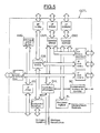
- Access to the communication bus is managed by a block ABG global arbitration scheme in the control circuit (FIG. 5) and by a local arbitration block in each interface circuit of the emulator.
- a block of the control circuit can therefore communicate with a block of the reconfigurable interface circuit in a transparent manner, that is to say as if it were part of the control circuit.
- Many arbitration mechanisms can be used to determine which block material will take hold at some point. For example, a arbitration mechanism may be to rotate priorities each cycle of the communication bus so that an access request the bus always ends up being served.
- the control circuit also includes the control part of a hardware logical analyzer AL.
- This block consists of one or several programmable logic controllers whose state evolves according to the predefined or programmable triggers produced by the circuit reconfigurable interface of the CRFG emulator, as well as a set counters and internal flags.
- This hardware block allows control a simulation sequence and make the most of the trace memories that we make based on the memories static or dynamic connected to the control circuit.
- the analyzer logic thus formed takes up the general characteristics of a conventional logic analyzer except that it has the properties reconfigurations of the reconfigurable interface circuit to achieve a hardware trace monitor and triggers.
- a clock controller CHL is synchronized by a clock basic system (or primary clock) that can also serve advantageously, to clock the communication bus of the test bench reconfigurable.
- the clock controller produces groups of secondary clock signals, corresponding to the clocks of the circuit under test and to the clocks of the various pilots / instructors and pilot / monitor interfaces found in the circuit (s) reconfigurable interface with the emulator.
- the clock controller CHL can also receive clocks from the system as input target when the circuit under test is fully synchronized or for partly by external clocks.
- the clock controller includes several generators independent signals providing secondary clocks.
- the secondary clocks produced by a generator are interrelated according to determined frequency and phase ratios.
- Each generator can communicate with different hardware blocks of the bench reconfigurable test to determine the progress of the clocks which it must provide to the circuit under test and to drivers / monitors. So a software driver can for example slow down a clock produced by a generator so that it adapts to its pacing rate, or a hardware trace driver can inhibit some secondary clocks from some generators for a certain period of time to perform a data transfer from the trace memory to the host computer.
- a BC block of combination of control signals centralizes control signals coming from or going to the different hardware blocks involved in the control of the clocks.
- SDRAM dynamic memory CSD controller enables to read or write the dynamic memories connected to the circuit of CCTL control from host computer or circuit reconfigurable interface CRFG.
- a controller CSR SRAM static memory allows you to read or write static memories connected to the control circuit CCTL from the host computer or CRFG reconfigurable interface circuit.
- these memories are used to sample the data from the interface bus with the CRFG reconfigurable interface emulator.
- These memories can also be used for other purposes such as memorizing different configurations of the circuit under test emulator, keep test vectors or software applications executed by a hardware model of a complete system.
- the control circuit CCTL also includes an interface JTAG compliant IFG test kit for fast access to the map resources from the host computer and this, without go through an external cable. Such an interface can be used from a classic way to perform production tests by checking in particular the quality of the connections between the different components of the map. This interface also serves, when starting the card, for identify the reconfigurable circuits used on the platform.
- the CCTL control block also features an interface IFCF configuration and replay, which allows you to configure or reread the configuration of the various reconfigurable circuits of the emulation system.
- a CIS in-situ controller allows the implementation of in-circuit emulation by booting the IFSC external interface circuit and controlling the communication between the emulated circuit under test and the target system.
- control circuit CCTL includes interfaces I / F to different components external to the control circuit.
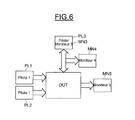
- this one is modeled as a set of PLi and MNi drivers / monitors interacting with the circuit under test DUT.
- PLi drivers are used to boost the circuit under test while MNi monitors are used to observe, that is, to analyze the response of the circuit under test.
- the drivers / monitors are user-defined at different levels of abstraction (material description, programs, %) and correspond to software or hardware models.
- the goal is to accelerate only the circuit under test but also the biggest part of the test environment.
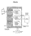
- FIG. 7a schematically illustrates the general structure of the reconfigurable test bench BTR where the different pilots / instructors and interface of pilots / monitors of the environment test.
- the fixed part of the reconfigurable test bench performs interfacing functions with the host computer and the system target and that it also realizes the functions of a logic analyzer.
- variable part that is to say, reconfigurable, realizes the part hardware emulated from the test environment that we can see as a set of hardware blocks interfacing with the circuit under test to stimulate and observe it. These hardware blocks communicate by elsewhere through different buses with the OH host computer the system SYC target and the actual additional hardware resources of the fixed part of the BTR reconfigurable test bench.
- the associated hardware blocks mobilize only material resources emulated or real and they do not do not necessarily communicate with the host computer when they stimulate and observe the circuit under test.
- FIG. 7b illustrates the contents of the reconfigurable circuit interface CRFG.
- This reconfigurable interface circuit includes pre-defined hardware blocks (or system modules) such as bus interfaces connected to the CCTL control circuit or the local ABL arbitration block and it also has hardware blocks variables that are generated based on the drivers / monitors used in the test environment.
- the internal communication bus of the test bench reconfigurable is extended in the reconfigurable interface circuit CRFG.
- Some hardware blocks of the reconfigurable interface circuit CRFGs such as software / driver interfaces and block calculating hardware triggers can thus access in a way transparent to the internal communication bus.
- An arbitration block local ABL determines access to the communication bus based on requests from the hardware blocks that are connected to it.
- a hardware triggers calculation block integrates both programmable triggers making simple comparisons between one or more signals of the interface bus with the emulator and a logical state given, and triggers generated at compile time in according to the needs in terms of logical analysis. It can be by example of a comparison between two vectorized signals of the bus interface with the emulator.
- This trigger calculation block material can be considered as the hardware block of a monitor hardware of the circuit under test, even if this monitor does not appear explicitly in the original test environment.
- a CSC block of combination of the control signals centralises the control signals coming from or going to different blocks materials involved in the control of clocks and communicated with block BC of the control circuit CCTL.
- the reconfigurable interface circuit CRFG then comprises the hardware blocks corresponding to the pilot / monitor interfaces and pilots / instructors needed to stimulate and observe the circuit under test.
- these hardware blocks are connected fully or for part of the interface bus with the emulator.
- the interface bus with the emulator can also be used to convey signals between blocks hardware, which allows the debugging of pilots / instructors emulated hardware or transponders (pilot / monitor interfaces transaction level software) by re-using the same means of debugging only those of the circuit under test.
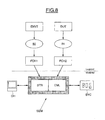
- Figure 8 shows a general mode of implementation of the emulation method according to the invention.
- a first file is generated FCH1 configuration to configure the test bench reconfigurable, and more precisely the CRFG reconfigurable circuit.
- the generation step 800 of the logic circuit will also provide a database of references for the simulation, which will enable the software to know how to initialize the test bench reconfigurable and how to communicate with the test bench reconfigurable to boost / observe the circuit under test and finally retrieve some results from the simulation.
- the GenFW generator therefore loads fixed netlists corresponding to pilots / instructors qualified as “static” or netlists generated on the fly (or dynamically) by modules software and corresponding to qualified pilots / instructors of "Dynamic".
- Static driver / monitor netlists and modules software invoked by GenFW to produce the netlists of Dynamic drivers / monitors are provided with GenFW, or are developed by the user or by a third party.
- the GenFW generator also builds the hardware block to combine some control signals and the hardware block corresponding to the hardware triggers. He finally assembles all hardware blocks provided or generated to produce the logic circuit in the form of a network of doors that will serve as a basis for the reconfiguration of the reconfigurable test bench and more particularly reconfigurable CRFG interface circuit.
- the reference database for the simulation contains different files produced by both the software modules of generation of drivers / monitors netlist and GenFW generator.
- the generation of the logic circuit is also in charge of performing the assignment of input-output of the circuit under test to the pins of the emulator of circuit under test.
- the generation of the logic circuit then uses input parameter a description of the interface of the circuit under test, which can come for example in the form of a netlist representing the entire circuit under test or simply the interface of the model of highest level.
- Assigning the I / O of the circuit under test to the pins of the emulators can be made in a random or in a more deterministic way by applying heuristics to obtain a more optimal assignments.
- the generation of the logic circuit outputs instructions from compilation for the circuit under test through scripts of compilation and description of the input / output assignment logic of the circuit under test at the pins of the emulator, this output description being otherwise a constraint parameter for the compilation of the circuit under test on the emulator.
- GenFW generation means will be designated by their reference GenFW, and the circuit under test will be designated by its reference DUT.
- the compilation of the DUT by the XILINX compilation software provides a file extension ".pad", assignment of the inputs and outputs of the DUT to the pins of the reconfigurable emulation circuit.
- This file contains the list of its inputs-outputs, with their direction and the physical pin of the reconfigurable circuit (FPGA) on which they are assigned. Taking this information into account allows GenFW to correctly place the input-output of the reconfigurable test bench by generating an assignment of I / O of the logic circuit for the reconfigurable circuit interface CRFG. This assignment is produced in the form an ".ucf" extension file, describing the constraints for the Xilinx compilation software.
- the structure of the test environment is described by a ".dve" extension file, listing the drivers / monitors instantiated in the test environment and the definition of the hardware triggers. For each driver / monitor, this file describes the connection to the DUT and possibly to other drivers / monitors (this also including the hardware triggers calculation block) according to a syntax similar to the Verilog language. It also contains the various parameters ('defparam' directives) which allow to configure each driver / monitor and to define on which clocks a driver / monitor synchronizes.
- 'defparam' directives which allow to configure each driver / monitor and to define on which clocks a driver / monitor synchronizes.
- a circuit is stimulated by an emulated hardware driver whose model name is 'randomModel'.
- the file ".dve” indicates under which name the driver model must be instantiated in the logical circuit ('randgen') and how the driver is connected to circuit under test. So the 'clk' connector of the driver is connected to the clock 'c1k0' of the circuit under test, and the connector 'val' is connected to the vectorized input 'din' of this same circuit under test.
- Trigger 'trigger0' is defined as an OR function on the signals 'din [0]' and 'din [1]', so that 'trigger0' is active when one of the two signals 'din [0]' or 'din [1]' is active.
- test environment could as well be described by a material description in a language such as VHDL or Verilog.
- the ".dve" file can be itself automatically generated by the GenFW program in based on the description of the interface of the circuit under test.
- GenFW supports instantiation of drivers / monitors hardware or software directly supplied with the system of emulation according to the invention, but also of pilots / instructors developed by the user or by third parties.
- a typical case of driver / monitor developed by the user corresponds to the driver / monitor hardware emulated. The user simply provides an EDIF netlist of its pilot / monitor, which will be instantiated by GenFW in the reconfigurable CRFG interface circuit.
- a case typical driver / monitor developed by third parties transactors.
- the software driver / monitor interface transactional can come either directly in the form of a netlist EDIF, either can be generated by a software module according to certain parameters defined in the ".dve" file.
- GenFW must so be able to invoke such a software module with its good parameters and be able to retrieve the resulting netlist EDIF for insert it into the CRFG reconfigurable interface circuit.
- GenFW makes it possible to implement a generic approach where each driver / monitor hardware block is handled in a way indifferent, regardless of its characteristics, of whom the designs and how it is produced.
- Some drivers / monitors are provided with the emulation system according to the invention but others can be developed by the user or a third party.
- Each driver / monitor is linked to a directory that contains information necessary for the eventual generation and the use of the hardware block to be inserted into the circuit reconfigurable interface CRFG.
- This directory contains in particular an ".install" extension file that indicates the type driver / monitor (static / dynamic) and the method of production of the netlist in the case of a pilot / monitor dynamic.
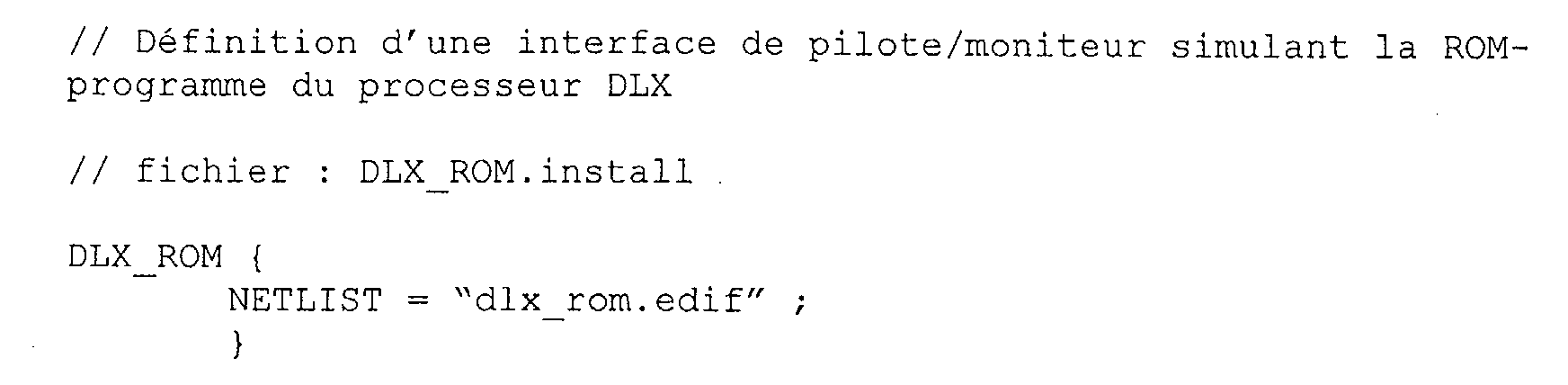
- the file ".install” indicates the name of the netlist file EDIF to load in genFW, in this case 'dlx _ rom.edif'.
- a dynamic driver / monitor is built by a software module capable of generating the EDIF netlist to be inserted in the CRFG reconfigurable interface circuit.
- the software module corresponds to a script file, an executable program, one or more files describing a hardware model to be synthesized, or a dynamically loadable library in GenFW.
- the software module must have an entry point so that GenFW can invoke the generation of the netlist of the driver / monitor hardware block with some generation parameters.
- this generation function is called by GenFW by providing as parameters all the information relating to an instantiation of the driver / monitor as described in the ".dve” file.
- An example ".install" file for a dynamic driver / monitor is given below:
- the software module is described as a library dynamic ('genCCosim.so') to which GenFW will bind dynamically.
- the entry point of the software module is the function 'genCCosimNetlist' which is called by GenFW with a particular prototype.
- This prototype has as a parameter the structure of data representing the instantiation of the pilot / monitor in the ".dve" (instance name, DUT connections, directives 'Defparam ).
- the function provides a netlist to GenFW that takes care of instantiate it in the netlist of reconfigurable interface circuit CRFG.
- the software module (through the function 'genCCosimNetlist') can also provide information from complete the database of references for the simulation.
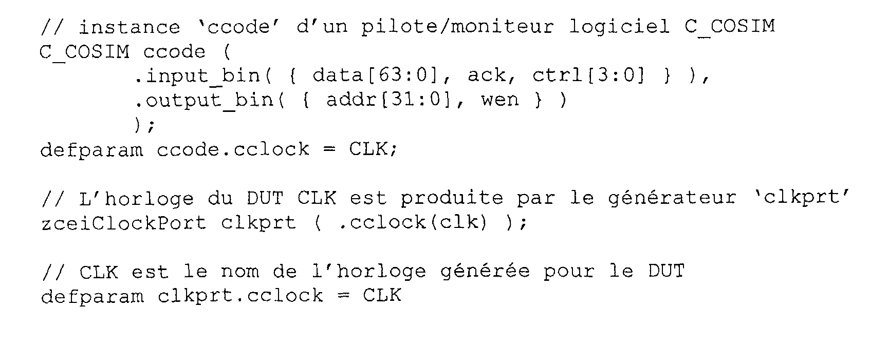
- the cosimulation driver / monitor generator C produces a C (or C ++) file that contains the data structures and functions needed by the user to stimulate, from a C (or C ++) application, the signals from the DUT that he connected to the pilot / cosimulation monitor (Explicit connections in the ".dve” extension file).
- GenFW finally produces a netlist in EDIF format for the logic circuit, which serves as a basis for configuring the reconfigurable CRFG interface circuit.
- This netlist includes the description and realizes interconnection of the different hardware blocks of drivers / monitors and system modules.
- GenFW also produces a ".ucf" extension file to express the input-output placement constraints of the logic circuit on the CRFG reconfigurable interface circuit.
- This file intended for the Xilinx compilation software, contains also time constraints (in particular for the blocks interface of the reconfigurable circuit CRFG with the circuit of CCTL control).
- GenFW also generates the file containing the list hardware blocks introduced in the netlist of the logic circuit realized by the reconfigurable interface circuit CRFG and requiring an interaction (initialization or communication) with the software.
- Figure 10 schematically illustrates the architecture of a hardware block corresponding to an interface of driver / software monitor.
- the architecture of software driver / monitor interfaces and connection semantics take up some principles of the SCE-MI standard, but this one has been adapted to be able to establish communication with the software at bit / signal level.
- the hardware block of a driver / monitor interface software contains a CTIF module that communicates on one side with the DUT (depending on the connections that have been explicitly described in file ".dve") and on the other side with the communication bus the reconfigurable test bench through particular cells called "ports" of communication.
- Fig. 11 illustrates an example of a hardware block for a static software driver / monitor interface 'dlx _ rom'.
- the software driver / monitor 'dlx _ rom' is used to stimulate the DUT (in this case a DLX processor) by software simulating the operation of a read-only memory (ROM) containing the DLX program.
- ROM read-only memory
- the first line 'defparam' of the file ".dve” means that the clock generated by the generator 'ZceiClockPort' is called also 'DLX_CLK'.
- the second line 'defparam' means that this clock 'DLX_CLK' is retro-controlled by the driver / monitor software 'dlx_rom' which indicates that the circuit under test will operate at a frequency determined by the pacing speed of the driver / monitor.
- the following example illustrates the case of a dynamic software driver / monitor with ports of varying size.
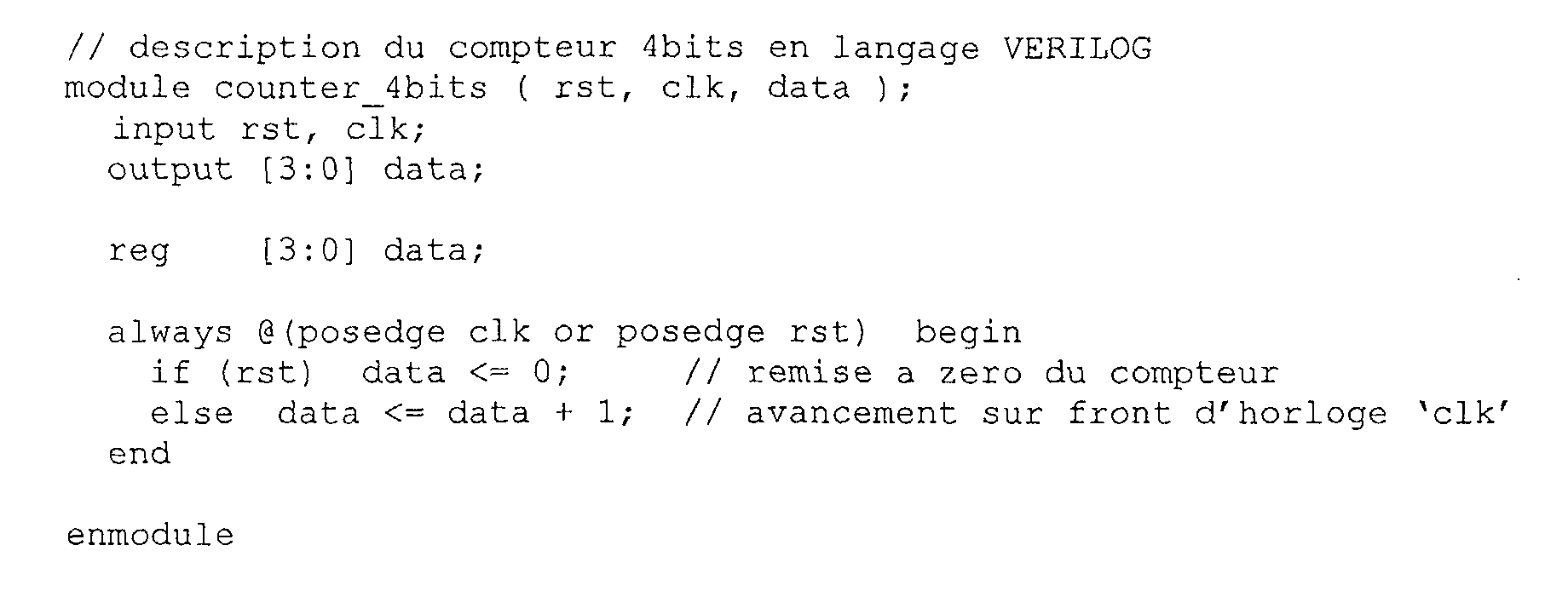
- the DUT circuit to emulate with the emulation system according to the invention is a 4-bit counter described in verilog language.
- the user must then implement a tool for logical synthesis (for example the one known under the name leonardo of the company MENTOR GRAPHICS) to transform the VERILOG description of the counter in a netlist EDIF.
- the netlist EDIF obtained will be called 'counter_4bits.edf' in the sequel of the example.
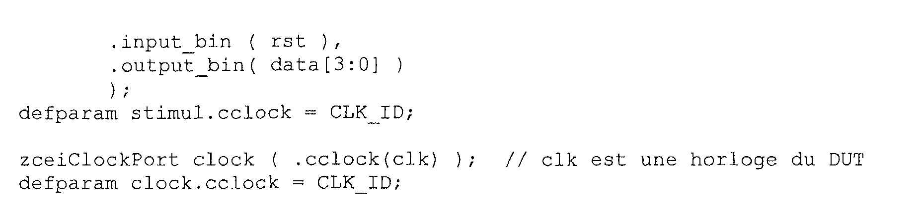
- test environment has only one driver / monitor corresponding to a program in C / C ++ made by the user.
- This file means that the user of the emulation system according to the invention wants to control the signal value 'rst' of delivery to zero of the DUT, as well as the advancement of the clock 'clk' in his C / C ++ program.
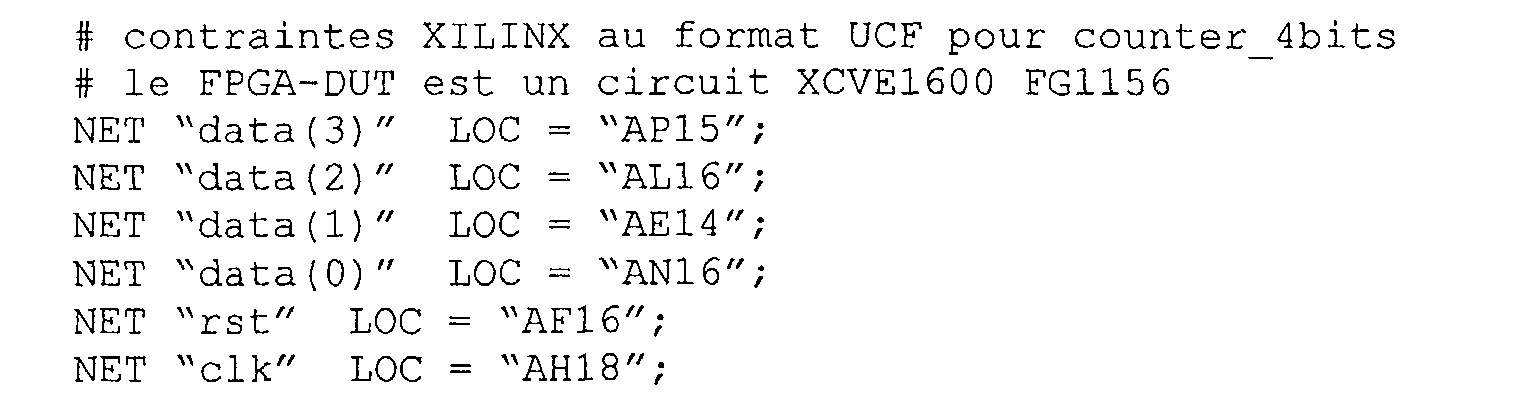
- the 'counter_4bits.ucf' file produced by GenFW contains the constraints of placement of the inputs / outputs of the DUT on the reconfigurable circuit pins forming the EML emulator, which is for example an FPGA circuit designated in the following under the term FPGA DUT.
- reconfigurable circuit CRFG is referred to as FPGA FP.
- the UCF format used is a proprietary format of XILINX.
- AP15, AL16, ..., AH18 are names of FPGA DUT pins, conforming to the XILINX nomenclature.
- GenFW chose FPGA DUT pins that are connected to the reconfigurable test bench BTR (so that the bench BTR test can control the inputs / outputs of the DUT).
- pin AH18 used for input 'clk' is a pin of the FPGA DUT clock: GenFW decided to place 'clk' on one of the FPGA DUT clock networks from the instantiation of the 'zceiClockPort' in the file 'Counter_4bits.dve.
- the FPGA DUT is a VIRTEX-E circuit 1600 to housing 1156 pins; the names of the pins chosen by GenFW are compatible with this type of FPGA. Use another FPGA model would likely have resulted in a different choice of pins.
- the file 'fp_firmware.edf' is the EDIF netlist of FPGA FP of reconfigurable test bench. It contains the instance 'stimul' of the costimulation pilot / monitor C 'C_COSIM' according to what has been described previously.
- the file 'fp_firmware.ucf' contains the compilation constraints of the netlist of the CRFG reconfigurable circuit by the XILINX compilation software. As the extract below shows, the constraints describe the placement of the input-output signals of the logic circuit CCL on the FPGA FP pins, but also time constraints such as the minimum frequency required for the system clock. the reconfigurable test bench.
- the FPGA FP is a VIRTEX-E circuit 1600 to 900 pin housing; the names of the pins chosen by GenFW are compatible with this type of FPGA. Use another FPGA model would likely result in a different choice of pins.
- the file 'fp_firmware.xref' is intended for the interface with the software. It indicates the resources inserted into the reconfigurable test bench allowing control of the emulation system by the program running on the host computer.
- FIG. 12a To describe a MRCH clock feedback means. Indeed while the circuit under test and some pilots / monitors (usually from hardware type) can operate at high frequencies (10MHz for example), other pilots / monitors (usually software type) can not only not work such frequencies in continuous mode but moreover can not to stimulate / observe the circuit under test at a constant frequency and pre-determined.
- two pilot interfaces software P1 and P2 operating on average respectively at 10kHz and 500kHz were represented, as well as a monitor emulated material MI that can reach a maximum frequency of 12 MHz operation.
- the MRCH means consisting of doors logic receive the clock signal driverClock issued by the clock divider DH clocked by the basic clock signal systemClock.
- the division factor is determined so that that the clock frequency driverClock can not exceed the maximum operating frequency of the circuit under test emulated and hardware drivers / monitors.
- the MRCH means also receive two signals waiting w1 and w2 issued by the two pilots P1 and P2, and deliver to the two software drivers their respective clock signals ckp1, ckp2, and the hardware monitor Ml and the circuit emulator under EML test the ckEML clock signal.
- Figure 12b shows a table describing the behavior outputs of the MRCH block according to its inputs.
- the waiting signal w1 is at 1 (active)
- the signals ckp2 and ckEML are stopped, but the ckpl clock still remains active (this can be the direct or split driverClock clock).
- the waiting signal w2 is at 1 (active)
- the signals ckpl and ckEML are stopped, but the ckp2 clock still remains active (this can be the direct or split driverClock clock).
- the number of signals can be reduced clocks used in the test environment by using activation signals on the driverClock clock, since when secondary clocks are active, they all derive clock driverClock.
- the signal generator clocks MRCH synchronized by the basic system clock divided, delivers different secondary clock signals synchronizing the emulator of the circuit under test and some at least hardware resources of the test bench.
- the means of clock feedback are then able in response to at least a waiting signal emitted by one of the material means of the bank of test clocked by a first secondary clock signal, to inhibit temporarily some of the other secondary clock signals different frequencies from that of the first clock signal secondary.
Landscapes
- Engineering & Computer Science (AREA)
- General Engineering & Computer Science (AREA)
- Computer Hardware Design (AREA)
- Physics & Mathematics (AREA)
- General Physics & Mathematics (AREA)
- Theoretical Computer Science (AREA)
- Quality & Reliability (AREA)
- Evolutionary Computation (AREA)
- Geometry (AREA)
- Test And Diagnosis Of Digital Computers (AREA)
- Tests Of Electronic Circuits (AREA)
Abstract
Description
- environnement de test à base de vecteurs de test embarqués dans le système reconfigurable : les vecteurs de test peuvent être stockés dans une ou plusieurs mémoires du système reconfigurable et un comparateur logique est mis en oeuvre pour comparer les sorties du circuit sous test avec les sorties attendues,
- environnement de test constitué d'un modèle matériel synthétisable embarqué dans le système reconfigurable : l'environnement de test peut être décrit par un modèle matériel que l'on peut émuler et donc implanter directement dans le système reconfigurable,
- environnement de test constitué d'un modèle matériel simulé sur l'ordinateur hôte : l'environnement de test peut être décrit par un modèle matériel que l'on va simuler (il n'est pas synthétisable) sur l'ordinateur hôte. Un lien entre l'ordinateur hôte et le système reconfigurable permet d'assurer la communication entre l'environnement de test simulé et le circuit sous test émulé.
- la figure 1 illustre schématiquement un mode de réalisation d'un système d'émulation selon l'invention,
- la figure 2 illustre un mode de réalisation du système d'émulation selon l'invention lorsque le banc de test reconfigurable et l'émulateur sont intégrés dans l'ordinateur hôte,
- la figure 3 illustre plus en détail, mais toujours de façon schématique, une architecture générale d'un banc de test reconfigurable selon l'invention,
- la figure 4 illustre plus en détail une partie de la figure 3,
- la figure 5 illustre schématiquement un mode de réalisation d'un circuit de contrôle d'un banc de test reconfigurable
- la figure 6 illustre schématiquement un exemple d'environnement de test pour un circuit sous test,
- la figure 7a illustre schématiquement une autre représentation d'un banc de test reconfigurable selon l'invention,
- la figure 7b illustre schématiquement un mode de réalisation d'un circuit reconfigurable d'interface d'un banc de test reconfigurable
- la figure 8 représente schématiquement un mode de mise en oeuvre d'un procédé d'émulation selon l'invention,
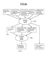
- la figure 9a illustre plus en détail un flot général de génération de la configuration d'un banc de test reconfigurable dans le cas où le circuit sous test a déjà été compilé sur son émulateur,
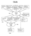
- La figure 9b illustre plus en détail un flot général de génération de la configuration d'un banc de test reconfigurable dans le cas où le circuit sous test n'a pas encore été compilé sur son émulateur,
- les figures 10 et 11 illustrent une représentation de modules pilotes,
- la figure 12a illustre schématiquement un mode de réalisation de moyens de rétrocontrôle d'horloge selon l'invention, et
- La figure 12b illustre sous la forme d'une table le comportement de la circuiterie de rétro-contrôle mise en oeuvre pour la figure 12a.
une partie centrale CR comportant, comme on le verra plus en détails ci-après, au moins un circuit de contrôle et au moins un circuit reconfigurable,
un générateur d'horloge GH, et
des circuits de mémoire statique et/ou dynamique CMM.
- Interface de pilotes/moniteurs logiciels : il s'agit des interfaces de pilotes/moniteurs de stimulation logicielle établissant une communication avec un processus logiciel exécuté sur l'ordinateur hôte ;
- Pilotes/moniteurs matériels émulés : il s'agit de pilotes/moniteurs de stimulation matérielle qui sont directement émulées dans le banc de test reconfigurable.
- Interfaces de pilotes/moniteurs matériels réels: il s'agit des interfaces de pilotes/moniteurs de stimulation matérielle réelle établissant une communication avec des ressources matérielles du banc de test reconfigurable, ou avec un système externe, tel que le système cible
- la génération 800 d'un circuit logique CCL constitué d'un réseau de portes logiques (ou netlist) représentatives de l'environnement de test, ainsi que des directives de compilation, et
- une compilation 801 de ce circuit logique CCL compte tenu desdites directives, de façon à obtenir le fichier de configuration FCH1 qui va permettre de configurer le banc de test reconfigurable.
- description de l'assignation des entrées/sorties logiques du circuit sous test aux broches de l'émulateur,
- description de la structure de l'environnement de test: il s'agit de la manière dont les pilotes/moniteurs sont connectés au circuit sous test (ceux-ci incluant aussi les horloges), avec d'éventuels paramètres définissant les conditions d'utilisation de ces pilotes/moniteurs, et par ailleurs la définition des déclencheurs pré-définis,
- des netlists de pilotes/moniteurs statiques : il s'agit des pilotes/moniteurs dont le bloc matériel à inclure dans le circuit reconfigurable d'interface CRFG, est fourni directement sous la forme d'un réseau de portes,
- des constructeurs de netlists de pilotes/moniteurs dynamiques : il s'agit des pilotes/moniteurs dont le bloc matériel à inclure dans le circuit reconfigurable d'interface CRFG, est produit sous la forme d'un réseau de portes par un module logiciel appelé dynamiquement par le générateur GenFW
- des modules système : ce sont les blocs matériels pré-définis nécessaires à l'intégration des blocs matériels des pilotes/moniteurs dans le banc de test reconfigurable.
- la netlist décrivant le circuit logique,
- des directives de compilation du circuit logique, c'est à
dire :
- des scripts automatisant la compilation du circuit logique et des contraintes temporelles et/ou de placement pour assurer le fonctionnement, du circuit logique à une fréquence élevée
- une assignation des entrées/sorties du circuit logique aux broches du circuit reconfigurable d'interface CRFG
- une base de donnée de référence nécessaire à la simulation permettant au logiciel de communiquer d'une manière générale avec le banc de test reconfigurable


- la liste des horloges utilisées par le circuit sous test et les pilotes/moniteurs de l'environnement de test
- la liste des pilotes/moniteurs ayant un accès au bus de communication du banc de test reconfigurable. L'accès au bus est mis en oeuvre par un ou plusieurs ports de communication (en émission et réception) présents dans la netlist du bloc matériel de chaque pilote/moniteur.
- ZceiMessageInPort : permet l'envoi de messages depuis le logiciel vers le module CTIF
- ZceiMessageOutPort : permet l'envoi de messages depuis le module CTIF vers le logiciel,
- ZceiClockControl : permet de contrôler l'avancement de l'horloge appliquée au DUT (appelé aussi mécanisme de « rétro-contrôle ») et qui est aussi associée au pilote/moniteur.
- de relier les connecteurs de la netlist aux signaux internes du circuit logique, et en particulier au bus de d'interface avec l'émulateur de sorte que la netlist soit finalement relié aux connecteurs du circuit sous test conformément aux indications du fichier d'extension ".dve"
- de remplacer les boites noires ZceiMessageInPort et ZceiMessageOutPort par des modules connectés au bus de communication du circuit reconfigurable CRFG, lui même étant une extension locale du bus de communication du circuit de contrôle CCTL, et donc permettant l'échange de données avec le logiciel
- de remplacer les boites noires ZceiClockControl par de la logique connectée à des ports externes du circuit reconfigurable CRFG;
- dlx_rom_data : vecteur de 32 sorties qui fournit au DLX les données lues dans la mémoire.
- dlx_rom_addr : vecteur de 32 entrées qui génère l'adresse mémoire que veut lire le DLX.
- dlx_rom_cen : une entrée dont la fonction est la sélection de la mémoire par le DLX.
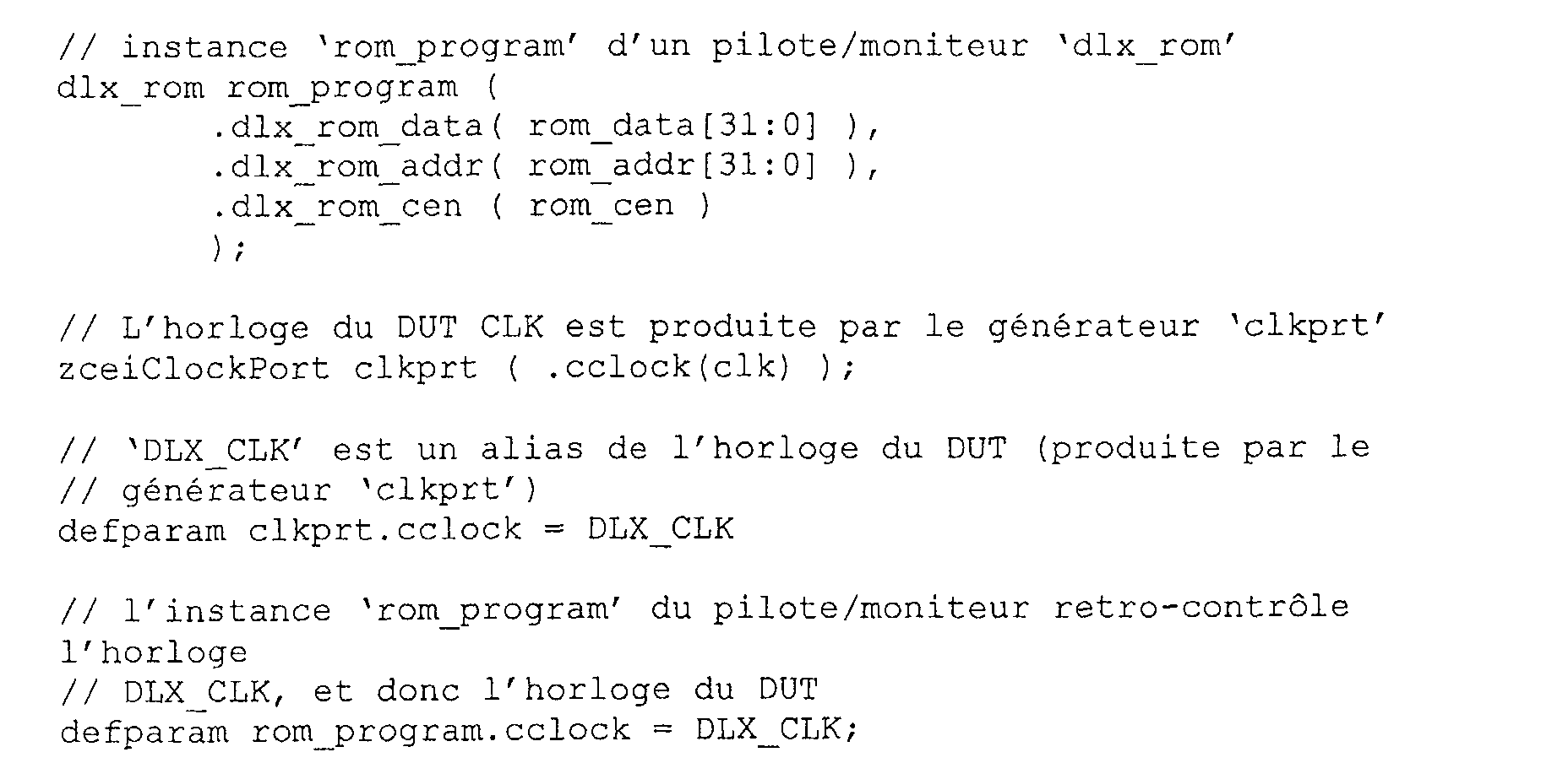
- qu'il faut créer une instance nommée 'rom_program' du modèle 'dlx_rom' dans le circuit logique
- que le vecteur de connecteurs 'd1x_rom_data' de l'instance 'rom_program' doit être connecté aux signaux d'entrées 'rom_data[31]' à 'rom_data[0]' du DUT, qui sont accessibles par le bus d'interface avec l'émulateur.
- que le vecteur de connecteurs 'd1x_rom_addr' de l'instance 'rom_program' doit être connecté aux signaux de sortie 'rom_addr[31]' à 'rom_addr[0]' du DUT qui sont accessibles par le bus d'interface avec l'émulateur.
- que le connecteur 'd1x_rom_cen' de l'instance 'rom_program' doit être connecté au signal de sortie 'rom_cen' du DUT qui est accessible par le bus d'interface avec l'émulateur.



- 'counter_4bits.edf' : la netlist EDIF du DUT,
- 'counter_4bits.dve' : la structure de l'environnement de test.
- 'fp_firmware.edf' : la netlist du circuit logique CCL (contenu du circuit reconfigurable CRFG),
- 'fp_firmware.ucf' : les contraintes de placement des entrées-sorties du circuit reconfigurable CRFG,
- 'fp_firmware.xref' : données pour le logiciel de simulation,
- 'counter_4bits.ucf' : les contraintes de placement des entrées-sorties du circuit reconfigurable formant l'émulateur EML,
- 'stimul.c' : fichier C pour la mise en oeuvre du pilote/moniteur de cosimulation dans le programme C/C++ de l'utilisateur.
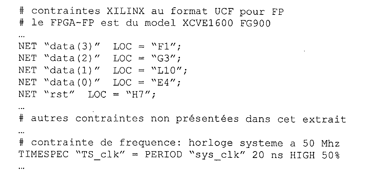
- la broche 'F1' du FPGA FP et reliée à la broche 'AP15' du FPGA DUT
- la broche 'G3' du FPGA FP et reliée à la broche 'AL16' du FPGA DUT
- la broche 'L10' du FPGA FP et reliée à la broche 'AE14' du FPGA DUT
- la broche 'E4' du FPGA FP et reliée à la broche 'AN16' du FPGA DUT
- la broche 'H7' du FPGA FP et reliée à la broche 'AF16' du FPGA DUT.
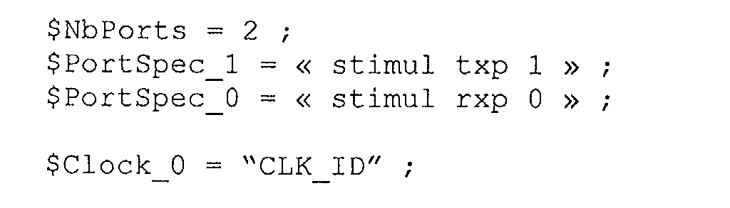
- port 0 (déclaration $PortSpec_0) : port 'rxp' du pilote/moniteur 'stimul' instancié dans le fichier ".dve"
- port 1 (déclaration $PortSpec_1) : port 'txp' du pilote/moniteur 'stimul' instancié dans le fichier ".dve"
Claims (25)
- Procédé d'émulation d'un circuit sous test associé à un environnement de test, caractérisé par le fait qu'il comporte deux phases distinctes de génération comportant une première phase de génération (80) d'un premier fichier (FCH1) de configuration de l'environnement de test, et une deuxième phase de génération (81) d'un deuxième fichier (FCH2) de configuration d'au moins une partie du circuit sous test, la délivrance du premier fichier de configuration à une première partie matérielle reconfigurable (BTR) formant un banc de test reconfigurable de façon à configurer le banc de test, et la délivrance du deuxième fichier de configuration à une deuxième partie matérielle reconfigurable (EML) de façon à configurer un émulateur du circuit sous test, les deux parties matérielles étant distinctes et mutuellement connectées.
- Procédé selon la revendication 1, caractérisé par le fait que la première phase de génération (80) comporte la production (800) d'un circuit logique (CRL) constitué d'un réseau de portes logiques et représentatif de l'environnement de test ainsi que des directives de compilation, et une compilation (801) de ce circuit logique compte tenu desdites directives, de façon à obtenir ledit premier fichier de configuration (FCH1).
- Procédé selon la revendication 2, caractérisé par le fait que l'environnement de test comporte un ensemble de pilotes (PLi) et de moniteurs (MNi), et par le fait que la production dudit circuit logique comporte la formation de blocs matériels sous la forme de réseaux de portes logiques, ces blocs matériels représentant des interfaces de pilotes/moniteurs de stimulation logicielle, des interfaces de pilotes/moniteurs de stimulation matérielle réelle, et des pilotes/moniteurs de stimulation matérielle émulée, des blocs de calculs de déclencheurs matériels, ainsi qu'un bloc d'interface avec l'émulateur du circuit sous test.
- Procédé selon la revendication 3, caractérisé par le fait que la phase de formation des blocs matériels se fait à partir de réseaux de portes définis statiquement ou de réseaux de portes générés dynamiquement par un module logiciel.
- Procédé selon l'une des revendications précédentes, caractérisé par le fait que la première phase de génération (80) et la deuxième phase de génération (81) sont effectuées en parallèle.
- Procédé selon l'une des revendications 1 à 4, caractérisé par le fait que la première phase de génération (80) et la deuxième phase de génération (81) sont effectuées séquentiellement.
- Procédé selon la revendication 6, caractérisé par le fait qu'on effectue la première phase de génération (80) avant ou après la deuxième phase de génération (81).
- Procédé selon les revendications 3 et 7, caractérisé par le fait que lorsque la première phase de génération est effectuée après la deuxième phase de génération, la production du circuit logique (CRL) utilise comme paramètres d'entrée une description de l'assignation des entrées/sorties logiques du circuit sous test aux broches de l'émulateur, et par le fait que lorsque la deuxième phase de génération est effectuée après la première phase de génération, la production du circuit logique utilise comme paramètres d'entrée une description de l'interface du circuit sous test et fournit en sortie une description de l'assignation des entrées/sorties logiques du circuit sous test aux broches de l'émulateur, cette description de sortie étant alors un paramètre de contrainte pour la deuxième phase de génération.
- Système d'émulation, destiné à émuler un circuit sous test associé à un environnement de test, caractérisé par le fait qu'il comporte un banc de test matériel reconfigurable (BTR) capable d'émuler une partie au moins de l'environnement de test, ce banc de test étant connecté entre un ordinateur hôte et un émulateur matériel reconfigurable (EML), distinct du banc de test, et capable d'émuler au moins une partie du circuit sous test, des premiers moyens de génération aptes à générer un premier fichier de configuration de l'environnement de test, et des deuxièmes moyens de génération aptes à générer un deuxième fichier de configuration du circuit sous test.
- Système selon la revendication 9, caractérisé par le fait que le banc de test reconfigurable (BTR) comporte une partie dite fixe et au moins un circuit reconfigurable d'interface (CRFG) capable de réaliser la partie émulée de l'environnement de test.
- Système selon la revendication 10, caractérisé par le fait que la partie fixe comporte au moins un circuit de contrôle (CCTL) et un circuit d'interface (CIBS) avec l'ordinateur hôte, et par le fait que le circuit reconfigurable d'interface est apte à comporter au moins des interfaces de pilotes/moniteurs de stimulation logicielle capables d'établir une communication avec au moins un processus logiciel exécuté sur l'ordinateur hôte, et des pilotes/moniteurs de stimulation matérielle émulée.
- Système selon la revendication 11, caractérisé par le fait que la partie fixe comporte en outre des pilotes/moniteurs matériels réels supplémentaires, et par le fait que le circuit reconfigurable (CRFG) est apte à comporter en outre des interfaces avec ces pilotes/moniteurs matériels réels supplémentaires.
- Système selon l'une des revendications 9 à 12, caractérisé par le fait que la partie fixe comporte en outre un circuit d'interface (IFSC) avec un dispositif cible (SYC).
- Système selon l'une des revendications 9 à 13, caractérisé par le fait que la partie fixe comporte en outre la partie contrôle d'un analyseur logique matériel (AL) dont l'état évolue en fonction de déclencheurs matériels.
- Système selon l'une des revendications 9 à 14, caractérisé par le fait que le banc de test reconfigurable comporte un générateur de signaux d'horloges, synchronisé par une horloge système de base et délivrant différents signaux d'horloge secondaires synchronisant l'émulateur du circuit sous test et certains au moins des moyens matériels du banc de test, ainsi que des moyens de rétrocontrôle d'horloge capable en réponse à au moins un signal d'attente émis par l'un des moyens matériels du banc de test cadencé par un premier signal d'horloge secondaire, d'inhiber temporairement certains des autres signaux d'horloge secondaires de fréquences différentes de celle du premier signal d'horloge secondaire.
- Système selon l'une des revendications 9 à 15, caractérisé par le fait que le banc de test et l'émulateur sont réalisés sur une carte électronique externe à l'ordinateur hôte et connectée à la carte mère de celui-ci.
- Système selon l'une des revendications 9 à 15, caractérisé par le fait que le banc de test reconfigurable est réalisé sur une première carte électronique externe à l'ordinateur hôte et connectée à la carte mère de celui-ci, et par le fait que l'émulateur du circuit sous test est réalisé sur une ou plusieurs autres cartes externes à l'ordinateur hôte connectées à ladite première carte externe.
- Système selon la revendication 17, caractérisé par le fait que le circuit d'interface avec le dispositif cible est intégré à ladite première carte externe.
- Système selon l'une des revendications 10 à 16, caractérisé par le fait que le banc de test et l'émulateur sont réalisés sur une carte électronique interne (CINT) incorporée dans l'ordinateur hôte.
- Système selon les revendications 13 et 19, caractérisé par le fait que le circuit d'interface avec le dispositif cible est réalisé sur une carte électronique externe (CXT) à l'ordinateur hôte, et apte à être connectée à ladite carte électronique interne (CINT).
- Carte électronique, destinée à être connectée à la carte mère d'un ordinateur hôte, caractérisée par le fait qu'elle comporte un banc de test matériel reconfigurable (BTR) capable d'émuler une partie au moins d'un environnement de test associé à un circuit sous test, et un émulateur matériel reconfigurable (EML), distinct du banc de test, connecté au banc de test reconfigurable et capable d'émuler au moins une partie du circuit sous test.
- Carte selon la revendication 21, caractérisée par le fait que le banc de test reconfigurable (BTR) comporte une partie dite fixe et au moins un circuit reconfigurable capable de réaliser la partie émulée de l'environnement de test.
- Carte selon la revendication 22, caractérisée par le fait que la partie fixe comporte au moins un circuit de contrôle (CCTL) et un circuit d'interface avec l'ordinateur hôte, et par le fait que le circuit reconfigurable est apte à comporter au moins des interfaces de pilotes/moniteurs de stimulation logicielle capables d'établir une communication avec au moins un processus logiciel exécuté sur l'ordinateur hôte, et des pilotes/moniteurs de stimulation matérielle émulée.
- Carte selon la revendication 23, caractérisée par le fait que la partie fixe comporte en outre des pilotes/moniteurs matériels réels supplémentaires, et par le fait que le circuit reconfigurable est apte à comporter en outre des interfaces avec ces pilotes/moniteurs matériels réels supplémentaires.
- Carte selon l'une des revendications 21 à 24, caractérisée par le fait que le banc de test reconfigurable comporte un générateur de signaux d'horloges, synchronisé par une horloge système de base et délivrant différents signaux d'horloge secondaires de fréquences différentes, ainsi que des moyens de rétrocontrôle d'horloge capable en réponse à un signal d'attente émis par l'un des moyens matériels du banc de test cadencé par un premier signal d'horloge secondaire, d'inhiber temporairement les signaux d'horloge secondaires de fréquences différentes de celle du premier signal d'horloge secondaire.
Applications Claiming Priority (2)
| Application Number | Priority Date | Filing Date | Title |
|---|---|---|---|
| FR0207949A FR2841668B1 (fr) | 2002-06-26 | 2002-06-26 | Procede et systeme d'emulation d'un circuit sous test associe a un environnement de test |
| FR0207949 | 2002-06-26 |
Publications (2)
| Publication Number | Publication Date |
|---|---|
| EP1376417A1 true EP1376417A1 (fr) | 2004-01-02 |
| EP1376417B1 EP1376417B1 (fr) | 2016-09-07 |
Family
ID=29717108
Family Applications (1)
| Application Number | Title | Priority Date | Filing Date |
|---|---|---|---|
| EP03291452.5A Expired - Lifetime EP1376417B1 (fr) | 2002-06-26 | 2003-06-16 | Procédé et système d'émulation d'un circuit sous test associé à un environnement de test |
Country Status (3)
| Country | Link |
|---|---|
| US (2) | US20040111252A1 (fr) |
| EP (1) | EP1376417B1 (fr) |
| FR (1) | FR2841668B1 (fr) |
Cited By (5)
| Publication number | Priority date | Publication date | Assignee | Title |
|---|---|---|---|---|
| EP1600865A1 (fr) * | 2004-05-28 | 2005-11-30 | Quickturn Design Systems, Inc. | Programmation dynamique de conditions de déclenchement dans des systèmes d'émulation de matériel |
| CN101963933A (zh) * | 2010-09-29 | 2011-02-02 | 清华大学 | 仪器测试中适应多通信协议的仪器静态匹配方法 |
| CN101517391B (zh) * | 2006-09-27 | 2011-08-10 | Ifp公司 | 与发动机试验台类型无关的发动机试验台监控系统 |
| CN115659885A (zh) * | 2022-12-29 | 2023-01-31 | 摩尔线程智能科技(北京)有限责任公司 | 仿真测试的系统和方法 |
| CN116243618A (zh) * | 2022-12-19 | 2023-06-09 | 中国航天空气动力技术研究院 | 一种基于nipxi设备和fpga板卡的产品测试仿真系统 |
Families Citing this family (37)
| Publication number | Priority date | Publication date | Assignee | Title |
|---|---|---|---|---|
| US7072818B1 (en) * | 1999-11-30 | 2006-07-04 | Synplicity, Inc. | Method and system for debugging an electronic system |
| US7065481B2 (en) * | 1999-11-30 | 2006-06-20 | Synplicity, Inc. | Method and system for debugging an electronic system using instrumentation circuitry and a logic analyzer |
| US7240303B1 (en) | 1999-11-30 | 2007-07-03 | Synplicity, Inc. | Hardware/software co-debugging in a hardware description language |
| US7222315B2 (en) * | 2000-11-28 | 2007-05-22 | Synplicity, Inc. | Hardware-based HDL code coverage and design analysis |
| US7827510B1 (en) | 2002-06-07 | 2010-11-02 | Synopsys, Inc. | Enhanced hardware debugging with embedded FPGAS in a hardware description language |
| EP1447759A1 (fr) * | 2003-02-07 | 2004-08-18 | ARM Limited | Génération de banc d'essai pour representer un dispositif |
| US6839242B2 (en) * | 2003-02-13 | 2005-01-04 | Rincon Research Corporation | Reconfigurable circuit modules |
| US7418678B1 (en) * | 2003-12-01 | 2008-08-26 | Jasper Design Automation, Inc. | Managing formal verification complexity of designs with counters |
| US7257802B2 (en) * | 2003-12-29 | 2007-08-14 | Mentor Graphics Corporation | Method and system for hardware accelerated verification of digital circuit design and its testbench |
| US7260798B2 (en) * | 2003-12-29 | 2007-08-21 | Mentor Graphics Corporation | Compilation of remote procedure calls between a timed HDL model on a reconfigurable hardware platform and an untimed model on a sequential computing platform |
| US7305332B1 (en) * | 2004-01-14 | 2007-12-04 | Adaptec, Inc. | System and method for automatic extraction of testing information from a functional specification |
| US8171472B1 (en) * | 2007-08-08 | 2012-05-01 | Sprint Communications Company L.P. | Separation and reuse of versions directory in execution framework installations |
| US7930165B2 (en) * | 2008-02-07 | 2011-04-19 | Accemic Gmbh & Co. Kg | Procedure and device for emulating a programmable unit providing system integrity control |
| CN101996148B (zh) * | 2010-09-29 | 2012-07-18 | 清华大学 | 用于多种通信协议的仪器测试板卡配置方法 |
| TWI450118B (zh) * | 2010-11-02 | 2014-08-21 | Global Unichip Corp | 混合的電子設計系統及其可重組連接矩陣 |
| CN104133745A (zh) * | 2013-04-30 | 2014-11-05 | 鸿富锦精密工业(深圳)有限公司 | 具有测试功能的电子装置及测试方法和系统 |
| US9075624B2 (en) * | 2013-06-24 | 2015-07-07 | Xilinx, Inc. | Compilation of system designs |
| US9152520B2 (en) * | 2013-09-26 | 2015-10-06 | Texas Instruments Incorporated | Programmable interface-based validation and debug |
| US9239899B2 (en) | 2014-03-11 | 2016-01-19 | Wipro Limited | System and method for improved transaction based verification of design under test (DUT) to minimize bogus fails |
| WO2016066950A1 (fr) * | 2014-10-30 | 2016-05-06 | Spherea Test & Services | Banc et logiciel pour tester un appareillage electrique, notamment un calculateur |
| US9773078B2 (en) | 2015-01-22 | 2017-09-26 | Synopsys, Inc. | X-propagation in emulation using efficient memory |
| US9659118B2 (en) | 2015-01-22 | 2017-05-23 | Synopsys, Inc. | X-propagation in emulation |
| WO2016118204A1 (fr) * | 2015-01-22 | 2016-07-28 | Synopsys, Inc. | Propagation x en émulation |
| US9684492B2 (en) * | 2015-09-28 | 2017-06-20 | Semmle Limited | Automatic determination of compiler configuration |
| US10185794B2 (en) * | 2015-10-20 | 2019-01-22 | Synopsys, Inc. | Overlaying of clock and data propagation in emulation |
| US10671785B1 (en) * | 2016-12-06 | 2020-06-02 | Xilinx, Inc. | Framework for reusing cores in simulation |
| US10198539B1 (en) * | 2017-03-02 | 2019-02-05 | Cadence Design Systems, Inc. | Systems and methods for dynamic RTL monitors in emulation systems |
| US11194943B2 (en) * | 2017-12-12 | 2021-12-07 | Synopsys, Inc. | FPGA-based hardware emulator system with an inter-FPGA connection switch |
| WO2019167081A1 (fr) * | 2018-03-02 | 2019-09-06 | Apasangi Akash | Système et procédé d'émulation et de simulation de rtl (conception à l'essai) à l'aide d'un fpga |
| US11080446B2 (en) * | 2019-03-18 | 2021-08-03 | Synopsys, Inc. | Method to regulate clock frequencies of hybrid electronic systems |
| US10990425B2 (en) * | 2019-05-08 | 2021-04-27 | Morgan Stanley Services Group Inc. | Simulated change of immutable objects during execution runtime |
| CN111310313B (zh) * | 2020-01-21 | 2023-10-13 | 北京北方华创微电子装备有限公司 | 基于iap的仿真模拟方法、装置以及晶圆清洗设备 |
| KR102213842B1 (ko) * | 2020-10-20 | 2021-02-08 | 국방과학연구소 | 무기체계 환경/신뢰성 시험용 이종 시험장비 인터페이스 장치, 환경시험 시스템, 및 데이터 중간 장치 |
| CN114706758B (zh) * | 2022-03-09 | 2025-03-18 | 西安智周深鉴信息科技集团有限公司 | 仿真测试的脚本生成方法、电子设备及存储介质 |
| CN116401018A (zh) * | 2023-04-14 | 2023-07-07 | 北京计算机技术及应用研究所 | 基于通用计算平台的嵌入式软件仿真目标机构建方法 |
| CN116736088B (zh) * | 2023-08-11 | 2023-11-17 | 上海类比半导体技术有限公司 | 一种用于协助硅后测试的芯片测试方法 |
| CN117521583B (zh) * | 2023-11-17 | 2024-07-19 | 中科苏州智能计算技术研究院 | 一种时钟驱动的软硬件联合仿真方法、系统及存储介质 |
Citations (1)
| Publication number | Priority date | Publication date | Assignee | Title |
|---|---|---|---|---|
| US6347388B1 (en) * | 1997-06-03 | 2002-02-12 | Verisity Ltd. | Method and apparatus for test generation during circuit design |
Family Cites Families (16)
| Publication number | Priority date | Publication date | Assignee | Title |
|---|---|---|---|---|
| US6389379B1 (en) * | 1997-05-02 | 2002-05-14 | Axis Systems, Inc. | Converification system and method |
| US5960191A (en) * | 1997-05-30 | 1999-09-28 | Quickturn Design Systems, Inc. | Emulation system with time-multiplexed interconnect |
| US6338158B1 (en) * | 1997-10-31 | 2002-01-08 | Vlsi Technology, Inc. | Custom IC hardware modeling using standard ICs for use in IC design validation |
| US6298320B1 (en) * | 1998-02-17 | 2001-10-02 | Applied Microsystems Corporation | System and method for testing an embedded microprocessor system containing physical and/or simulated hardware |
| US6223144B1 (en) * | 1998-03-24 | 2001-04-24 | Advanced Technology Materials, Inc. | Method and apparatus for evaluating software programs for semiconductor circuits |
| US6279146B1 (en) * | 1999-01-06 | 2001-08-21 | Simutech Corporation | Apparatus and method for verifying a multi-component electronic design |
| US6298452B1 (en) * | 1999-02-05 | 2001-10-02 | Hewlett-Packard Company | Hardware test coverage using inter-chip event filtering in multi-chip simulations |
| US6332201B1 (en) * | 1999-03-23 | 2001-12-18 | Hewlett-Packard Company | Test results checking via predictive-reactive emulation |
| US6272451B1 (en) * | 1999-07-16 | 2001-08-07 | Atmel Corporation | Software tool to allow field programmable system level devices |
| US6473726B1 (en) * | 1999-09-24 | 2002-10-29 | Frederic Reblewski | Method and apparatus for concurrent emulation of multiple circuit designs on an emulation system |
| US6611796B1 (en) * | 1999-10-20 | 2003-08-26 | Texas Instruments Incorporated | Method and apparatus for combining memory blocks for in circuit emulation |
| US6678645B1 (en) * | 1999-10-28 | 2004-01-13 | Advantest Corp. | Method and apparatus for SoC design validation |
| US6618839B1 (en) * | 1999-11-30 | 2003-09-09 | Synplicity, Inc. | Method and system for providing an electronic system design with enhanced debugging capabilities |
| US6587995B1 (en) * | 2000-04-19 | 2003-07-01 | Koninklijke Philips Electronics N.V. | Enhanced programmable core model with integrated graphical debugging functionality |
| US6611936B2 (en) * | 2000-04-28 | 2003-08-26 | Hewlett-Packard Development Company, L.P. | Programmable delay elements for source synchronous link function design verification through simulation |
| WO2001086513A2 (fr) * | 2000-05-11 | 2001-11-15 | Quickturn Design Systems, Inc. | Circuit d'emulation avec un algorithme d'heure de remise en file, un analyseur logique et une memoire fantome |
-
2002
- 2002-06-26 FR FR0207949A patent/FR2841668B1/fr not_active Expired - Fee Related
-
2003
- 2003-06-16 EP EP03291452.5A patent/EP1376417B1/fr not_active Expired - Lifetime
- 2003-06-26 US US10/603,776 patent/US20040111252A1/en not_active Abandoned
-
2009
- 2009-07-22 US US12/507,612 patent/US20100161306A1/en not_active Abandoned
Patent Citations (1)
| Publication number | Priority date | Publication date | Assignee | Title |
|---|---|---|---|---|
| US6347388B1 (en) * | 1997-06-03 | 2002-02-12 | Verisity Ltd. | Method and apparatus for test generation during circuit design |
Non-Patent Citations (2)
| Title |
|---|
| HUTCHINGS B L ET AL: "Unifying simulation and execution in a design environment for FPGA systems", IEEE TRANS. VERY LARGE SCALE INTEGR. (VLSI) SYST. (USA), IEEE TRANSACTIONS ON VERY LARGE SCALE INTEGRATION (VLSI) SYSTEMS, FEB. 2001, IEEE, USA, vol. 9, no. 1, pages 201 - 205, XP002239439, ISSN: 1063-8210 * |
| NEALE R: "Verisity's eCelerator offers test bench synthesis", ELECTRONIC ENGINEERING DESIGN, APRIL 2002, CMP ELECTRONICS GROUP, UK, vol. 74, no. 903, pages 27 - 28, XP008016066, ISSN: 0013-4902 * |
Cited By (7)
| Publication number | Priority date | Publication date | Assignee | Title |
|---|---|---|---|---|
| EP1600865A1 (fr) * | 2004-05-28 | 2005-11-30 | Quickturn Design Systems, Inc. | Programmation dynamique de conditions de déclenchement dans des systèmes d'émulation de matériel |
| US7379861B2 (en) | 2004-05-28 | 2008-05-27 | Quickturn Design Systems, Inc. | Dynamic programming of trigger conditions in hardware emulation systems |
| CN101517391B (zh) * | 2006-09-27 | 2011-08-10 | Ifp公司 | 与发动机试验台类型无关的发动机试验台监控系统 |
| CN101963933A (zh) * | 2010-09-29 | 2011-02-02 | 清华大学 | 仪器测试中适应多通信协议的仪器静态匹配方法 |
| CN101963933B (zh) * | 2010-09-29 | 2012-11-14 | 清华大学 | 仪器测试中适应多通信协议的仪器静态匹配方法 |
| CN116243618A (zh) * | 2022-12-19 | 2023-06-09 | 中国航天空气动力技术研究院 | 一种基于nipxi设备和fpga板卡的产品测试仿真系统 |
| CN115659885A (zh) * | 2022-12-29 | 2023-01-31 | 摩尔线程智能科技(北京)有限责任公司 | 仿真测试的系统和方法 |
Also Published As
| Publication number | Publication date |
|---|---|
| EP1376417B1 (fr) | 2016-09-07 |
| FR2841668B1 (fr) | 2006-08-11 |
| US20100161306A1 (en) | 2010-06-24 |
| US20040111252A1 (en) | 2004-06-10 |
| FR2841668A1 (fr) | 2004-01-02 |
Similar Documents
| Publication | Publication Date | Title |
|---|---|---|
| EP1376417B1 (fr) | Procédé et système d'émulation d'un circuit sous test associé à un environnement de test | |
| JP7053691B2 (ja) | 多重プロセッサシステムのためのリアルタイム分析及び制御 | |
| US20210081258A1 (en) | Synthesis Path For Transforming Concurrent Programs Into Hardware Deployable on FPGA-Based Cloud Infrastructures | |
| EP0642683B1 (fr) | Procede et plate-formes de test pour le developpement d'un circuit integre | |
| US7340693B2 (en) | System for designing re-programmable digital hardware platforms | |
| EP1387304A1 (fr) | Procédé de vérification fonctionnelle d'un modèle de circuit intégré pour constituer une plate-forme de vérification, équipement émulateur et plate-forme de vérification | |
| EP1387305B1 (fr) | Procédé et systeme d'établissement automatique d'un modèle global de simulation d'une architecture | |
| Hardebolle et al. | Exploring multi-paradigm modeling techniques | |
| CN103324511B (zh) | 配置可编程设备的方法、可编程设备及机器可读存储介质 | |
| GB2318664A (en) | Embedded logic analyzer for a programmable logic device | |
| WO2008142355A2 (fr) | Procede de simulation d'un systeme embarque a bord d'un aeronef pour tester un logiciel de fonctionnement et dispositif pour la mise en oeuvre de ce procede | |
| CN116738901A (zh) | 一种芯片验证方法及装置 | |
| JP2731021B2 (ja) | Asic開発方法とasicエミュレータと集積回路の設計開発方法と単一集積回路の部分開発方法 | |
| EP0656591B1 (fr) | Simulateur de bus numérique intégré dans un système de test automatique | |
| EP2956874B1 (fr) | Dispositif et procédé pour accélérer la phase de mise à jour d'un noyau de simulation | |
| WO2006084845A2 (fr) | Procede de simulation d'un processeur utilisant un modele comprenant un ensemble de objets | |
| CN119720931B (zh) | 一种芯粒模拟平台设计方法、装置、电子设备及存储介质 | |
| de la Fuente et al. | Building a dynamically reconfigurable system through a high-level development flow | |
| Beserra et al. | Integrating virtual platforms into a heterogeneous MoC-based modeling framework | |
| De La Fuente et al. | Building a dynamically reconfigurable system through a high development flow | |
| Kent et al. | Robust adaptive modular perception system (RAMPS): A node-based processing framework for training and testing vehicle perception systems | |
| Gottschaldt et al. | KRS Unleashed: Towards a Robotics FPGA Development Environment for Rapid Prototyping | |
| EP1164487A1 (fr) | Dispositif de reproduction fonctionnelle d'un circuit intégré spécifique et son utilisation comme dispositif d'émulation | |
| Kritikakis et al. | Enabling dynamic system integration on MAXELER HLS platforms | |
| US20250068814A1 (en) | Instrumentation-assisted emulation debug of aspect-oriented hardware with mixed levels of abstraction |
Legal Events
| Date | Code | Title | Description |
|---|---|---|---|
| PUAI | Public reference made under article 153(3) epc to a published international application that has entered the european phase |
Free format text: ORIGINAL CODE: 0009012 |
|
| AK | Designated contracting states |
Kind code of ref document: A1 Designated state(s): AT BE BG CH CY CZ DE DK EE ES FI FR GB GR HU IE IT LI LU MC NL PT RO SE SI SK TR |
|
| AX | Request for extension of the european patent |
Extension state: AL LT LV MK |
|
| 17P | Request for examination filed |
Effective date: 20040617 |
|
| AKX | Designation fees paid |
Designated state(s): AT BE BG CH CY CZ DE DK EE ES FI FR GB GR HU IE IT LI LU MC NL PT RO SE SI SK TR |
|
| 17Q | First examination report despatched |
Effective date: 20061229 |
|
| RAP1 | Party data changed (applicant data changed or rights of an application transferred) |
Owner name: SYNOPSYS EMULATION AND VERIFICATION |
|
| REG | Reference to a national code |
Ref country code: DE Ref legal event code: R079 Ref document number: 60349360 Country of ref document: DE Free format text: PREVIOUS MAIN CLASS: G06F0017500000 Ipc: G06F0011260000 |
|
| RIC1 | Information provided on ipc code assigned before grant |
Ipc: G06F 11/26 20060101AFI20160317BHEP Ipc: G06F 17/50 20060101ALI20160317BHEP Ipc: G01R 31/3183 20060101ALI20160317BHEP |
|
| GRAP | Despatch of communication of intention to grant a patent |
Free format text: ORIGINAL CODE: EPIDOSNIGR1 |
|
| INTG | Intention to grant announced |
Effective date: 20160426 |
|
| GRAS | Grant fee paid |
Free format text: ORIGINAL CODE: EPIDOSNIGR3 |
|
| GRAA | (expected) grant |
Free format text: ORIGINAL CODE: 0009210 |
|
| AK | Designated contracting states |
Kind code of ref document: B1 Designated state(s): AT BE BG CH CY CZ DE DK EE ES FI FR GB GR HU IE IT LI LU MC NL PT RO SE SI SK TR |
|
| REG | Reference to a national code |
Ref country code: GB Ref legal event code: FG4D Free format text: NOT ENGLISH |
|
| REG | Reference to a national code |
Ref country code: CH Ref legal event code: EP |
|
| REG | Reference to a national code |
Ref country code: IE Ref legal event code: FG4D Free format text: LANGUAGE OF EP DOCUMENT: FRENCH |
|
| REG | Reference to a national code |
Ref country code: AT Ref legal event code: REF Ref document number: 827422 Country of ref document: AT Kind code of ref document: T Effective date: 20161015 |
|
| REG | Reference to a national code |
Ref country code: DE Ref legal event code: R096 Ref document number: 60349360 Country of ref document: DE |
|
| REG | Reference to a national code |
Ref country code: NL Ref legal event code: MP Effective date: 20160907 |
|
| PG25 | Lapsed in a contracting state [announced via postgrant information from national office to epo] |
Ref country code: FI Free format text: LAPSE BECAUSE OF FAILURE TO SUBMIT A TRANSLATION OF THE DESCRIPTION OR TO PAY THE FEE WITHIN THE PRESCRIBED TIME-LIMIT Effective date: 20160907 |
|
| REG | Reference to a national code |
Ref country code: AT Ref legal event code: MK05 Ref document number: 827422 Country of ref document: AT Kind code of ref document: T Effective date: 20160907 |
|
| PG25 | Lapsed in a contracting state [announced via postgrant information from national office to epo] |
Ref country code: NL Free format text: LAPSE BECAUSE OF FAILURE TO SUBMIT A TRANSLATION OF THE DESCRIPTION OR TO PAY THE FEE WITHIN THE PRESCRIBED TIME-LIMIT Effective date: 20160907 Ref country code: ES Free format text: LAPSE BECAUSE OF FAILURE TO SUBMIT A TRANSLATION OF THE DESCRIPTION OR TO PAY THE FEE WITHIN THE PRESCRIBED TIME-LIMIT Effective date: 20160907 Ref country code: GR Free format text: LAPSE BECAUSE OF FAILURE TO SUBMIT A TRANSLATION OF THE DESCRIPTION OR TO PAY THE FEE WITHIN THE PRESCRIBED TIME-LIMIT Effective date: 20161208 |
|
| PG25 | Lapsed in a contracting state [announced via postgrant information from national office to epo] |
Ref country code: EE Free format text: LAPSE BECAUSE OF FAILURE TO SUBMIT A TRANSLATION OF THE DESCRIPTION OR TO PAY THE FEE WITHIN THE PRESCRIBED TIME-LIMIT Effective date: 20160907 Ref country code: RO Free format text: LAPSE BECAUSE OF FAILURE TO SUBMIT A TRANSLATION OF THE DESCRIPTION OR TO PAY THE FEE WITHIN THE PRESCRIBED TIME-LIMIT Effective date: 20160907 |
|
| PG25 | Lapsed in a contracting state [announced via postgrant information from national office to epo] |
Ref country code: AT Free format text: LAPSE BECAUSE OF FAILURE TO SUBMIT A TRANSLATION OF THE DESCRIPTION OR TO PAY THE FEE WITHIN THE PRESCRIBED TIME-LIMIT Effective date: 20160907 Ref country code: BG Free format text: LAPSE BECAUSE OF FAILURE TO SUBMIT A TRANSLATION OF THE DESCRIPTION OR TO PAY THE FEE WITHIN THE PRESCRIBED TIME-LIMIT Effective date: 20161207 Ref country code: SK Free format text: LAPSE BECAUSE OF FAILURE TO SUBMIT A TRANSLATION OF THE DESCRIPTION OR TO PAY THE FEE WITHIN THE PRESCRIBED TIME-LIMIT Effective date: 20160907 Ref country code: PT Free format text: LAPSE BECAUSE OF FAILURE TO SUBMIT A TRANSLATION OF THE DESCRIPTION OR TO PAY THE FEE WITHIN THE PRESCRIBED TIME-LIMIT Effective date: 20170109 Ref country code: CZ Free format text: LAPSE BECAUSE OF FAILURE TO SUBMIT A TRANSLATION OF THE DESCRIPTION OR TO PAY THE FEE WITHIN THE PRESCRIBED TIME-LIMIT Effective date: 20160907 |
|
| REG | Reference to a national code |
Ref country code: DE Ref legal event code: R097 Ref document number: 60349360 Country of ref document: DE |
|
| PG25 | Lapsed in a contracting state [announced via postgrant information from national office to epo] |
Ref country code: IT Free format text: LAPSE BECAUSE OF FAILURE TO SUBMIT A TRANSLATION OF THE DESCRIPTION OR TO PAY THE FEE WITHIN THE PRESCRIBED TIME-LIMIT Effective date: 20160907 |
|
| PLBE | No opposition filed within time limit |
Free format text: ORIGINAL CODE: 0009261 |
|
| STAA | Information on the status of an ep patent application or granted ep patent |
Free format text: STATUS: NO OPPOSITION FILED WITHIN TIME LIMIT |
|
| PG25 | Lapsed in a contracting state [announced via postgrant information from national office to epo] |
Ref country code: DK Free format text: LAPSE BECAUSE OF FAILURE TO SUBMIT A TRANSLATION OF THE DESCRIPTION OR TO PAY THE FEE WITHIN THE PRESCRIBED TIME-LIMIT Effective date: 20160907 |
|
| 26N | No opposition filed |
Effective date: 20170608 |
|
| PG25 | Lapsed in a contracting state [announced via postgrant information from national office to epo] |
Ref country code: SI Free format text: LAPSE BECAUSE OF FAILURE TO SUBMIT A TRANSLATION OF THE DESCRIPTION OR TO PAY THE FEE WITHIN THE PRESCRIBED TIME-LIMIT Effective date: 20160907 |
|
| PG25 | Lapsed in a contracting state [announced via postgrant information from national office to epo] |
Ref country code: MC Free format text: LAPSE BECAUSE OF FAILURE TO SUBMIT A TRANSLATION OF THE DESCRIPTION OR TO PAY THE FEE WITHIN THE PRESCRIBED TIME-LIMIT Effective date: 20160907 |
|
| REG | Reference to a national code |
Ref country code: CH Ref legal event code: PL |
|
| GBPC | Gb: european patent ceased through non-payment of renewal fee |
Effective date: 20170616 |
|
| REG | Reference to a national code |
Ref country code: IE Ref legal event code: MM4A |
|
| REG | Reference to a national code |
Ref country code: FR Ref legal event code: ST Effective date: 20180228 |
|
| PG25 | Lapsed in a contracting state [announced via postgrant information from national office to epo] |
Ref country code: LI Free format text: LAPSE BECAUSE OF NON-PAYMENT OF DUE FEES Effective date: 20170630 Ref country code: CH Free format text: LAPSE BECAUSE OF NON-PAYMENT OF DUE FEES Effective date: 20170630 Ref country code: GB Free format text: LAPSE BECAUSE OF NON-PAYMENT OF DUE FEES Effective date: 20170616 Ref country code: LU Free format text: LAPSE BECAUSE OF NON-PAYMENT OF DUE FEES Effective date: 20170616 Ref country code: IE Free format text: LAPSE BECAUSE OF NON-PAYMENT OF DUE FEES Effective date: 20170616 |
|
| REG | Reference to a national code |
Ref country code: FR Ref legal event code: PLFP Year of fee payment: 15 |
|
| PG25 | Lapsed in a contracting state [announced via postgrant information from national office to epo] |
Ref country code: FR Free format text: LAPSE BECAUSE OF NON-PAYMENT OF DUE FEES Effective date: 20170630 |
|
| REG | Reference to a national code |
Ref country code: FR Ref legal event code: RN Effective date: 20180511 Ref country code: BE Ref legal event code: MM Effective date: 20170630 |
|
| PG25 | Lapsed in a contracting state [announced via postgrant information from national office to epo] |
Ref country code: BE Free format text: LAPSE BECAUSE OF NON-PAYMENT OF DUE FEES Effective date: 20170630 |
|
| REG | Reference to a national code |
Ref country code: FR Ref legal event code: PLFP Year of fee payment: 16 |
|
| REG | Reference to a national code |
Ref country code: FR Ref legal event code: FC Effective date: 20181009 |
|
| REG | Reference to a national code |
Ref country code: GB Ref legal event code: S28 Free format text: APPLICATION FILED |
|
| REG | Reference to a national code |
Ref country code: GB Ref legal event code: S28 Free format text: RESTORATION ALLOWED Effective date: 20190102 |
|
| PG25 | Lapsed in a contracting state [announced via postgrant information from national office to epo] |
Ref country code: FR Free format text: LAPSE BECAUSE OF NON-PAYMENT OF DUE FEES Effective date: 20170630 |
|
| PGRI | Patent reinstated in contracting state [announced from national office to epo] |
Ref country code: FR Effective date: 20181009 |
|
| PG25 | Lapsed in a contracting state [announced via postgrant information from national office to epo] |
Ref country code: HU Free format text: LAPSE BECAUSE OF FAILURE TO SUBMIT A TRANSLATION OF THE DESCRIPTION OR TO PAY THE FEE WITHIN THE PRESCRIBED TIME-LIMIT; INVALID AB INITIO Effective date: 20030616 |
|
| PG25 | Lapsed in a contracting state [announced via postgrant information from national office to epo] |
Ref country code: SE Free format text: LAPSE BECAUSE OF NON-PAYMENT OF DUE FEES Effective date: 20160907 |
|
| PG25 | Lapsed in a contracting state [announced via postgrant information from national office to epo] |
Ref country code: CY Free format text: LAPSE BECAUSE OF NON-PAYMENT OF DUE FEES Effective date: 20160907 |
|
| PG25 | Lapsed in a contracting state [announced via postgrant information from national office to epo] |
Ref country code: TR Free format text: LAPSE BECAUSE OF FAILURE TO SUBMIT A TRANSLATION OF THE DESCRIPTION OR TO PAY THE FEE WITHIN THE PRESCRIBED TIME-LIMIT Effective date: 20160907 |
|
| PGFP | Annual fee paid to national office [announced via postgrant information from national office to epo] |
Ref country code: GB Payment date: 20220519 Year of fee payment: 20 Ref country code: FR Payment date: 20220519 Year of fee payment: 20 Ref country code: DE Payment date: 20220518 Year of fee payment: 20 |
|
| REG | Reference to a national code |
Ref country code: DE Ref legal event code: R071 Ref document number: 60349360 Country of ref document: DE |
|
| REG | Reference to a national code |
Ref country code: GB Ref legal event code: PE20 Expiry date: 20230615 |
|
| P01 | Opt-out of the competence of the unified patent court (upc) registered |
Effective date: 20230528 |
|
| PG25 | Lapsed in a contracting state [announced via postgrant information from national office to epo] |
Ref country code: GB Free format text: LAPSE BECAUSE OF EXPIRATION OF PROTECTION Effective date: 20230615 |