EP1376178A2 - Integrated aspheric optical coupler for automatic photonics packaging - Google Patents
Integrated aspheric optical coupler for automatic photonics packaging Download PDFInfo
- Publication number
- EP1376178A2 EP1376178A2 EP03013578A EP03013578A EP1376178A2 EP 1376178 A2 EP1376178 A2 EP 1376178A2 EP 03013578 A EP03013578 A EP 03013578A EP 03013578 A EP03013578 A EP 03013578A EP 1376178 A2 EP1376178 A2 EP 1376178A2
- Authority
- EP
- European Patent Office
- Prior art keywords
- optical
- fiber
- substrate
- lens
- axis
- Prior art date
- Legal status (The legal status is an assumption and is not a legal conclusion. Google has not performed a legal analysis and makes no representation as to the accuracy of the status listed.)
- Withdrawn
Links
Images


Classifications
-
- G—PHYSICS
- G02—OPTICS
- G02B—OPTICAL ELEMENTS, SYSTEMS OR APPARATUS
- G02B6/00—Light guides; Structural details of arrangements comprising light guides and other optical elements, e.g. couplings
- G02B6/24—Coupling light guides
- G02B6/42—Coupling light guides with opto-electronic elements
Definitions
- the present invention relates, in general, to a photonics package incorporating a monolithically integrated alignment device for coupling optical energy between in-plane optical devices and to a method for producing the same. More specifically, the invention relates to a photonics package that incorporates an optical coupling and alignment device having an integral fiber groove, lens aperture and monolithic aspheric lens.
- Data in optical communication systems is often transmitted in the form of optical signals through an optical fiber terminating in a photonics device such as a receiver, transponder, transceiver, or the like.
- the data is projected from an optical fiber, for example as a light beam, directed onto a photonic die where the data is received by a photodetector and converted to a corresponding radio frequency (RF) electrical signal.
- RF radio frequency
- data can easily be lost due to improper alignment between the fiber and the photodetector or through light divergence, although both the alignment and divergence problems can be minimized where the fiber and the photodetector are in close proximity or where a lens can be used to focus the optical signal.
- these optical coupling systems are increasingly prevalent so that the need for simplified assembly processes for micro-optical coupling systems is increasingly important.
- an optical fiber is aligned to be perpendicular to a photodetector; in the second, the fiber is in-plane (i.e. parallel) to the photodetector.
- the photodetector and the fiber In the first construction, wherein light is projected from fiber directly onto the photodetector, the photodetector and the fiber must be optically aligned in three mutually perpendicular planes ((x-y), (x-z), and (y-z)), which complicates the assembly process.
- such an arrangement can be problematic for high frequency data transfer because it requires a longer wire bonding or transmission line, and this reduces device performance at high frequency operation.
- the optical signal from the fiber must be redirected in order to impinge on the photodetector.
- One known method for redirecting the optical signal in this type of alignment device is to reflect the optical signal off a mirror in a direction perpendicular to the axis of the fiber.
- Using a discrete mirror introduces an indirect connection between the fiber and photodetector, causing difficulty during alignment, raising costs due to the need for a more precise construction, and reducing reliability.
- the optical fiber holder has to incorporate a lens. Therefore, there are certain commercial advantages to eliminating the intermediate mirror.
- Another method for redirecting an optical signal from an optical fiber onto the surface of a plane perpendicular to the axis of the fiber involves cutting the terminal end of the fiber at an angle so that the signal in the fiber is deflected out in a direction approximately perpendicular to the axis. The fiber is then positioned so that the signal exiting the fiber passes through a lens, in order to align and focus the signal.
- This design is an improvement over prior devices, but since high frequency optical signals require miniscule photodetectors, the optical fiber must be in extremely close proximity to the photodetector to minimize light divergence and to maximize photodetector responsivity. Further, the three components; namely, the fiber, lens, and photodetector, have to be precisely located with respect to each other to ensure reliable coupling, and this is difficult to accomplish.
- the photonic package consists of several independently fabricated micro-optical components, including an optical fiber, a photodetector, a mirror, a lens and and a substrate or microbench on which the components are assembled, as well as bonding materials to connect the components, and frequently all were assembled manually, which is not efficient.
- automated assembly could be used, it fails to achieve the needed alignment precision. Accordingly, a simple construction for optically aligning a photodetector in a parallel orientation with an optical fiber is needed.
- the present invention relates to an improved photonics package for micro-optical systems, the package including an assembly for directing optical signals between first and second optical devices, one of which may be a source of such signals and the other of which may be a photodetector.
- the signals pass through an optical fiber and an optical coupler, or alignment device, to optically couple the fiber and a photonics die.
- a light source directs light into the optical fiber, and this fight is directed by the coupler to a photodetector on the die.
- the photonics package can be used to transmit light from a light transmitter on the die through the optical coupler to the optical fiber.
- the photonics package of the invention is formed by first fabricating a monolithic coupler, or alignment device from a substrate by a conventional etching process.
- the alignment device incorporates an integral fiber groove on its top surface, an integral aspheric lens, and an integral recessed receiver portion on its bottom surface for receiving a photonic die and for positioning it under the aspheric lens.
- the die includes a photodetector region which is located to receive an optical signal directed into the alignment device through an optical fiber placed in the fiber groove.
- the groove and fiber are generally parallel to the surface of the aspheric lens (i.e.
- the end of the fiber is cut at an angle to redirect an optical signal, propagating axially in the fiber, out of the fiber in a direction substantially perpendicular to the fiber's axis.
- the fiber cut may be polished and a high reflectivity coating added.
- the optical signal from the fiber is directed through, and is focused by, the aspheric lens and is received by the photodetector region on the precisely positioned photonic die.
- the photonic die may incorporate a light emitter, such as a vertical cavity surface emitting laser diode (VCSEL) or surface light emitting diode (SLED), aligned with the aspheric lens for directing light signals into the optical fiber by way of the angled terminal end of the fiber.
- VCSEL vertical cavity surface emitting laser diode
- SLED surface light emitting diode
- the monolithic alignment device with its included aspheric lens is fabricated within a substrate wafer by: 1) coating the substrate with a photoresist material for photolithographically patterning the substrate, 2) etching the substrate through the pattern using a standard semiconductor etching process to form a fiber groove on the top surface of the substrate and to form a top surface of the aspheric lens, 3) flipping the substrate over, and coating the bottom surface with a photoresist material for photolithography, 4) etching the bottom surface of the substrate, using a standard semiconductor etching process to form a recess on the bottom substrate surface and to form a bottom surface of the aspheric lens, and 5) coating both sides of the resulting aspheric lens with a thin film or film of material to make the input and output surfaces of the lens anti-reflective (AR).
- the preferred etching process is similar to that illustrated in U.S. Patent No. 5,853,960, which is hereby incorporated herein by reference
- a final step for fabricating the alignment device includes metalizing the fiber groove and the bottom of the substrate block, as with solder. Thereafter, an optical fiber having an angled terminal end is secured in the groove with the optical axis of the angled surface of the fiber aligned with the optical axis of the lens, and a photonic die is positioned in the recess so that a photodetector region or a surface light emitting active area on the die is aligned with the optical axis of the lens, and thus with the optical signal axis of the fiber.
- the monolithic alignment structure assures accurate and reliable alignment of the optical fiber, the lens, and the photodetector or surface light emitting device, and lends itself to automatic assembly procedures.
- the ability to form a monolithic, compact and simple optical coupling system for micro-optical devices has several advantages. For example, constructing all the components of an alignment device from identical material in a single process lowers assembly costs, reduces alignment problems during assembly and overcomes problems caused in earlier devices by unequal thermal expansion between components. Moreover, complex coupling and alignment schemes can be eliminated, reducing the number of components and the complexity of the process of manufacturing the device.
- a monolithic structure also permits a closer proximity of the fiber, tens, and photodetector light emitters, which allows for more accurate alignment, a decrease in the time required for alignment, and more efficient packaging of optical electronics systems. The assembly of the package can be automated, resulting in higher volume manufacturing and higher reproducibility.
- a monolithic micro-optical device incorporating a photonics package in accordance with the present invention efficiently addresses various problems associated with optical communication applications and improves upon the prior art by providing a commercially advantageous product.
- the device eliminates the need for manual assembly and improves reliability and accuracy by simplifying prior devices.
- Fig. 1 is a perspective view of a photonics package including an alignment device fabricated in accordance with the present invention
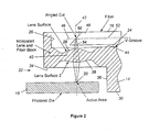
- Fig. 2 is a cross-sectional view taken along lines 2-2 of the photonics package of Fig. 1;
- Fig. 3 is a top plan view of the photonics package of Fig. 1;
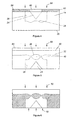
- Figs. 4-6 illustrate process steps for fabricating the device of Fig. 1.
- a photonics package 10 which includes a semiconductor monolithic optical coupler, or alignment device 12 fabricated from a substrate 14 by a standard semiconductor etching process. This process permits fabrication of the specific features needed for the alignment device 12, as will be described below.
- the photonics package 10 which may be used, for example, in a communications or data network application for converting optical signals to corresponding electrical signals, or vice-versa, includes the alignment device 12, an optical fiber 16 supported by the alignment device, and a photonic die 18 which includes an optically active region 20, which in one embodiment may be a photodetector. In another embodiment, the region 20 may instead be a light emitter such as a VCSEL or SLED.
- the alignment device 12 is a monolithic structure that is created (as further described below) from substrate 14 using conventional semiconductor fabrication techniques. The substrate is etched on its top surface to form a fiber groove 24, which may be generally V-shaped or U-shaped in cross-section, a lens aperture 26, and a top lens surface 28 within aperture 26.
- the bottom surface 30 of the substrate is etched to form a receiver section 32 which may be, in the preferred embodiment, in the form of an L-shaped groove or recess having a first, or horizontal, surface 34 and a second, or vertical surface 36 which forms a ledge or shoulder in the bottom of the substrate.
- the surface 34 is further etched to form a bottom lens surface 38.
- conventional photolithographic steps are used to self-align the top and bottom lens surfaces 28 and 38 to produce in the substrate an aspheric lens 40 centered in aperture 26 along lens axis 42.
- the receiver section 32 is precisely shaped and located during the etching process to receive the photonic die 18 and to position it so that its optically active region 20, which may be a light emitter or photodetector, is positioned in alignment with lens axis 42.
- its optically active region 20 which may be a light emitter or photodetector
- the receiver section preferably is shaped as needed to snugly receive and secure the die 18 in optical alignment with lens 40.
- the groove 24 in the top surface of the substrate is V-shaped in cross-section, although it may be generally U-shaped, with the base 44 of the groove aligned with, and by extension intersecting, the axis 42 of the lens.
- the V or U shape of the groove precisely aligns the longitudinal axis 46 of the optical fiber in the coupler so that axis 46 intersects lens axis 42.
- the terminal end 48 of the fiber 16 is cut, polished and HR coated with metals or other oxide materials. The cut is angled with respect to fiber axis 46 to produce an angled end surface 50 which redirects optical signals 52 propagating in the optical fiber out of the fiber, as a beam 54 in perpendicular alignment relative to the fiber's axis.
- the cut is preferably a forty-five degree angle with the axis of the fiber, although angles of between 35 and 54 degrees may be used.
- the end 48 of the fiber 16 is positioned in the lens aperture 26 so that the center, or axis, of surface 50 is aligned with lens axis 42, and the fiber is rotated so that the surface 50 directs beam 54 along axis 42 to pass through the lens 40.
- the lens 40 focuses the beam 54 onto the photonic die 18 containing a photodetector region 20. It will be understood that if the optically active region 20 is a surface light emitting device, then light from region 20 will be directed along the axis 42 of the lens into the fiber 16.
- a suitable light source (not shown) for supplying light to the couplerlalignment device 12 may be a laser source such as a diode laser, a photodiode, or the like coupled to fiber 16 either directly or through a suitable waveguide or additional optical fibers.
- the monolithic aspheric lens is fabricated within the substrate wafer by the process illustrated in Figs. 4-6.
- This process includes coating the top surface 58 of substrate 14 with a photoresist material 60 for photolithographically producing a pattern 62 on the substrate.
- the substrate is etched (arrows 64) using a standard semiconductor etching process to form the fiber groove 24, the aperture 26, and the top surface 28 of the aspheric lens 40 (Fig. 4).
- the substrate 14 is turned over (Fig.
- a final step includes metalizing the fiber groove and the bottom of the substrate block with solder, for example, to allow an optical fiber to be readily fastened to the coupler.
- the substrate 14 may be any high refractive index semiconductor, such as a Group III-V semiconductor, which has unique crystal planes that allow for preferential etching, and further may be, for example, Gallium Arsenide, Indium Arsenide, Gallium Phosphide, or Silicon (Si).
- the wafer consists of Indium Phosphide (InP).
- a silicon wafer preferably is used, followed by the a firing process after etching the substrate to smooth out the lens surface before the AR coating step.
- the substrate can take numerous shapes other than the generally rectangular shape illustrated, and the photonics package and alignment device could use some other mechanism for aligning and securing the fiber over the integrated lens.
- the type of lens formed on the semiconductor substrate wafer can be aspherical, semi-spherical, semi-cylindrical, Gausian-cylindrical, binary, Fresnell, refractive, or diffractive, as dictated by the mask pattern.
- the light source for the coupler could be a waveguide device, diode laser, optical fiber, photodiode, or optical integrated circuits.
Landscapes
- Physics & Mathematics (AREA)
- General Physics & Mathematics (AREA)
- Optics & Photonics (AREA)
- Optical Couplings Of Light Guides (AREA)
- Semiconductor Lasers (AREA)
- Light Receiving Elements (AREA)
Abstract
Description
Claims (10)
- A monolithic alignment device for a photonics package for coupling light between first and second optical devices, comprising:a substrate;a groove etched on a first side of said substrate for receiving a first optical device;an integrated lens etched in said substrate, said lens having an axis aligned with said groove and being located to allow an optical signal to pass between said first optical device on said first side of the substrate and a second side of the substrate along an optical path which includes said axis;a recess in a second side of said substrate for positioning a second optical device in said optical path.
- The alignment device as recited in claim 1, wherein said first optical device is an optical fiber propagating light from a source to said second optical device, and said second optical device includes a photodetector.
- The alignment device as recited in claim 1, wherein said first optical device is an optical fiber for receiving light from said second optical device, and said second optical device is a light emitting device.
- , The alignment device as recited in claim 1, wherein said substrate comprises a silicon material.
- The alignment device as recited in claim 1, wherein said substrate comprises a III-V semiconductor material.
- The alignment device as recited in claim 5, wherein the substrate comprises indium phosphide.
- The alignment device of claim 1, further including a lens aperture formed in said first side of said substrate, said integrated lens being integrally formed from said substrate in sald aperture, said lens being aspheric and having its optical axis extending through said substrate from said aperture to said recess on said second side of said substrate.
- The alignment device of claim 1 wherein said recess on said second side of said substrate is shaped to receive a photonics die incorporating an optical device and to align said optical device with said optical path.
- The alignment device of claim 1, wherein said first optical device is an optical fiber located in said groove, said fiber having a longitudinal axis and a sloped surface at a terminal end, said sloped surface and said longitudinal axis intersecting said optical axis, said sloped fiber surface being at an angle of between about 35° and about 54° with respect to said longitudinal axis of said fiber and with respect to said optical axis to direct optical signals between said fiber and said photodetector.
- The alignment device of claim 1, wherein said first optical device is an optical fiber located in said groove, said fiber having a longitudinal axis and a sloped surface at a terminal end, said sloped surface and said longitudinal axis intersecting said optical axis, said sloped fiber surface being at an angle of between about 35° and about 54° with respect to said longitudinal axis of said fiber and with respect to said optical axis to direct optical signals between said fiber and said photodetector.
Applications Claiming Priority (2)
| Application Number | Priority Date | Filing Date | Title |
|---|---|---|---|
| US170872 | 1980-07-21 | ||
| US10/170,872 US6965714B2 (en) | 2002-06-13 | 2002-06-13 | Integrated aspheric optical coupler for RF planarized automatic photonics packaging |
Publications (2)
| Publication Number | Publication Date |
|---|---|
| EP1376178A2 true EP1376178A2 (en) | 2004-01-02 |
| EP1376178A3 EP1376178A3 (en) | 2004-08-25 |
Family
ID=29717769
Family Applications (1)
| Application Number | Title | Priority Date | Filing Date |
|---|---|---|---|
| EP03013578A Withdrawn EP1376178A3 (en) | 2002-06-13 | 2003-06-13 | Integrated aspheric optical coupler for automatic photonics packaging |
Country Status (3)
| Country | Link |
|---|---|
| US (1) | US6965714B2 (en) |
| EP (1) | EP1376178A3 (en) |
| JP (1) | JP2004029798A (en) |
Cited By (2)
| Publication number | Priority date | Publication date | Assignee | Title |
|---|---|---|---|---|
| JP2012521570A (en) * | 2009-03-26 | 2012-09-13 | ウーハン・テレコミュニケーション・デバイシーズ・カンパニー・リミテッド | Transversely coupled optical fiber structural member and processing method thereof |
| US9651746B2 (en) | 2013-03-27 | 2017-05-16 | Ccs Technology, Inc. | Optoelectronic device and method for assembling an optoelectronic device |
Families Citing this family (28)
| Publication number | Priority date | Publication date | Assignee | Title |
|---|---|---|---|---|
| JP4166471B2 (en) * | 2001-12-28 | 2008-10-15 | 三菱電機株式会社 | Optical module |
| US7286743B2 (en) * | 2002-03-01 | 2007-10-23 | Jds Uniphase Corporation | High dynamic range integrated receiver |
| US6954580B2 (en) * | 2002-03-01 | 2005-10-11 | Jds Uniphase Corporation | Optical receiver with high dynamic range |
| US20060093271A1 (en) * | 2004-11-03 | 2006-05-04 | Fenwick David M | Optical connections and methods of forming optical connections |
| KR20060065430A (en) * | 2004-12-10 | 2006-06-14 | 한국전자통신연구원 | An optical fiber illumination system, a manufacturing method of the optical fiber illumination system, an optical recording head having an optical fiber illumination system, and an optical recording and reproducing apparatus |
| US7189007B2 (en) * | 2005-02-09 | 2007-03-13 | Tektronix, Inc. | Termination for optic fiber |
| US7943229B2 (en) * | 2005-05-06 | 2011-05-17 | Hoya Corporation Usa | Suppression of stray light propagation in a substrate |
| CN101351733B (en) * | 2005-12-28 | 2011-03-30 | 欧姆龙株式会社 | Optical module |
| JP5328095B2 (en) * | 2006-10-27 | 2013-10-30 | 京セラ株式会社 | Optical transmission board, opto-electronic hybrid board, optical module, and optoelectric circuit system |
| KR100860676B1 (en) * | 2007-01-11 | 2008-09-26 | 삼성전자주식회사 | Optical waveguide |
| US9229169B2 (en) * | 2011-08-16 | 2016-01-05 | International Business Machines Corporation | Lens array optical coupling to photonic chip |
| US8901576B2 (en) | 2012-01-18 | 2014-12-02 | International Business Machines Corporation | Silicon photonics wafer using standard silicon-on-insulator processes through substrate removal or transfer |
| MY178442A (en) * | 2012-09-11 | 2020-10-13 | Quantum Electro Opto Systems Sdn Bhd | Method and apparatus for optical coupling and opto-electronic conversion |
| US20140161385A1 (en) * | 2012-12-07 | 2014-06-12 | Telefonaktiebolaget Lm Ericsson (Publ) | Method and Apparatus for Coupling to an Optical Waveguide in a Silicon Photonics Die |
| CN103744147A (en) * | 2014-01-07 | 2014-04-23 | 西南科技大学 | Active optical cable optical coupling device with high coupling efficiency |
| CN104122634B (en) * | 2014-07-18 | 2016-06-08 | 中国科学院半导体研究所 | A kind of optically-coupled equipment being applied to opto-electronic device encapsulation |
| US9465175B2 (en) * | 2014-07-23 | 2016-10-11 | Sifotonics Technologies Co., Ltd. | Integrated lens-array-on-substrate for optical coupling system and fabrication method thereof |
| WO2016080296A1 (en) * | 2014-11-18 | 2016-05-26 | コニカミノルタ株式会社 | Optical path changing element and optical coupling device |
| US9791370B2 (en) * | 2015-04-14 | 2017-10-17 | Honeywell International Inc. | Die-integrated aspheric mirror |
| KR20190107528A (en) * | 2018-03-12 | 2019-09-20 | 한국전자통신연구원 | Method and device for determining state of optical network terminal line |
| JP6886432B2 (en) * | 2018-07-06 | 2021-06-16 | ライトラボ・イメージング・インコーポレーテッド | Fiber Optic Beam Directional Systems and Equipment |
| US11394468B2 (en) * | 2019-03-22 | 2022-07-19 | Source Photonics Inc. | System and method for transferring optical signals in photonic devices and method of making the system |
| CN114236710A (en) * | 2021-12-13 | 2022-03-25 | 无锡鑫巨宏智能科技有限公司 | High-speed coupling lens |
| CN114815094A (en) * | 2022-05-25 | 2022-07-29 | 中国电子科技集团公司第三十四研究所 | Method for coupling and aligning inclined optical fiber and detector chip |
| TWI864681B (en) * | 2023-04-17 | 2024-12-01 | 上詮光纖通信股份有限公司 | Light-coupling device |
| TWI882372B (en) * | 2023-06-29 | 2025-05-01 | 世界先進積體電路股份有限公司 | Photonic integrated circuit structure and fabrication method thereof |
| US12566295B2 (en) | 2023-08-31 | 2026-03-03 | Vanguard International Semiconductor Corporation | Photonic integrated circuit structure and fabrication method thereof |
| KR102843046B1 (en) * | 2024-12-20 | 2025-08-06 | 옵티시스 주식회사 | Multi-signal Transmit/Receive Optical Structure with Improved Manufacturing and Alignment Convenience |
Family Cites Families (6)
| Publication number | Priority date | Publication date | Assignee | Title |
|---|---|---|---|---|
| JPH05264869A (en) * | 1992-03-18 | 1993-10-15 | Fujitsu Ltd | Method for adjusting relative positional relation between optical fiber and photodetector to be optically coupled and evaluating method and device to be used for execution of these methods |
| US5471552A (en) * | 1995-02-22 | 1995-11-28 | Industrial Technology Research Institute | Fabrication of static-alignment fiber-guiding grooves for planar lightwave circuits |
| US5853960A (en) * | 1998-03-18 | 1998-12-29 | Trw Inc. | Method for producing a micro optical semiconductor lens |
| US6115521A (en) * | 1998-05-07 | 2000-09-05 | Trw Inc. | Fiber/waveguide-mirror-lens alignment device |
| US6205274B1 (en) | 1998-07-20 | 2001-03-20 | Honeywell Inc. | Fiber optic header for an edge emitting laser |
| US6243508B1 (en) * | 1999-06-01 | 2001-06-05 | Picolight Incorporated | Electro-opto-mechanical assembly for coupling a light source or receiver to an optical waveguide |
-
2002
- 2002-06-13 US US10/170,872 patent/US6965714B2/en not_active Expired - Lifetime
-
2003
- 2003-06-12 JP JP2003167755A patent/JP2004029798A/en active Pending
- 2003-06-13 EP EP03013578A patent/EP1376178A3/en not_active Withdrawn
Cited By (3)
| Publication number | Priority date | Publication date | Assignee | Title |
|---|---|---|---|---|
| JP2012521570A (en) * | 2009-03-26 | 2012-09-13 | ウーハン・テレコミュニケーション・デバイシーズ・カンパニー・リミテッド | Transversely coupled optical fiber structural member and processing method thereof |
| EP2413171A4 (en) * | 2009-03-26 | 2012-12-19 | Wuhan Telecomm Devices Co Ltd | Laterally coupled optical fiber component and processing method thereof |
| US9651746B2 (en) | 2013-03-27 | 2017-05-16 | Ccs Technology, Inc. | Optoelectronic device and method for assembling an optoelectronic device |
Also Published As
| Publication number | Publication date |
|---|---|
| US20030231828A1 (en) | 2003-12-18 |
| US6965714B2 (en) | 2005-11-15 |
| JP2004029798A (en) | 2004-01-29 |
| EP1376178A3 (en) | 2004-08-25 |
Similar Documents
| Publication | Publication Date | Title |
|---|---|---|
| US6965714B2 (en) | Integrated aspheric optical coupler for RF planarized automatic photonics packaging | |
| US6517257B2 (en) | Optical transmitter/receiver apparatus, method for fabricating the same and optical semiconductor module | |
| US6456761B2 (en) | Apparatus, assembly, and method for making micro-fixtured lensed assembly for optoelectronic devices and optical fibers | |
| US6316281B1 (en) | Method for fabricating a hybrid optical integrated circuit employing SOI optical waveguide | |
| KR100276968B1 (en) | Optical interconnection structure for enlarging alignment tolerance | |
| US9897769B2 (en) | Vision-based passive alignment of an optical fiber subassembly to an optoelectronic device | |
| KR100198460B1 (en) | Optical module with lens aligned in V-groove and method of making same | |
| US12379555B2 (en) | Detachable connector for co-packaged optics | |
| EP0660146B1 (en) | Light-receiving structure for waveguide type optical devices | |
| US6115521A (en) | Fiber/waveguide-mirror-lens alignment device | |
| US20060239612A1 (en) | Flip-chip devices formed on photonic integrated circuit chips | |
| US7050680B2 (en) | Optical coupling device having silicon optical bench and optical fiber with angled end face | |
| JP2000047055A (en) | Optical waveguide device and method of manufacturing the same | |
| US20240027703A1 (en) | Demountable connection of an optical connector using a foundation having features for integrated optical coupling and demountable mechanical coupling | |
| US6023546A (en) | Structure for securing optical device and fiber optics | |
| US20220260786A1 (en) | Optical Fiber Guide Structure and Optical Fiber Connecting Structure | |
| EP0887674A2 (en) | Optical transmitter/receiver apparatus, method for fabricating the same and optical semiconductor module | |
| JPH11149019A (en) | Optical transmitting / receiving device, method for manufacturing the same, and optical semiconductor module | |
| EP0846966A2 (en) | Optical waveguide | |
| US5224184A (en) | Optical multi-chip interconnect | |
| JPH11326662A (en) | Optical planar circuit | |
| EP1043608A1 (en) | Optical device and optical module with optical device | |
| JP2897742B2 (en) | Optical transceiver module | |
| JP2004157558A (en) | Optical semiconductor module | |
| JPH0667069A (en) | Photosemiconductor device |
Legal Events
| Date | Code | Title | Description |
|---|---|---|---|
| PUAI | Public reference made under article 153(3) epc to a published international application that has entered the european phase |
Free format text: ORIGINAL CODE: 0009012 |
|
| AK | Designated contracting states |
Kind code of ref document: A2 Designated state(s): AT BE BG CH CY CZ DE DK EE ES FI FR GB GR HU IE IT LI LU MC NL PT RO SE SI SK TR |
|
| AX | Request for extension of the european patent |
Extension state: AL LT LV MK |
|
| PUAL | Search report despatched |
Free format text: ORIGINAL CODE: 0009013 |
|
| AK | Designated contracting states |
Kind code of ref document: A3 Designated state(s): AT BE BG CH CY CZ DE DK EE ES FI FR GB GR HU IE IT LI LU MC NL PT RO SE SI SK TR |
|
| AX | Request for extension of the european patent |
Extension state: AL LT LV MK |
|
| 17P | Request for examination filed |
Effective date: 20050214 |
|
| AKX | Designation fees paid |
Designated state(s): DE FR GB SE |
|
| STAA | Information on the status of an ep patent application or granted ep patent |
Free format text: STATUS: THE APPLICATION IS DEEMED TO BE WITHDRAWN |
|
| 18D | Application deemed to be withdrawn |
Effective date: 20100105 |