Technical Field
The present invention relates to diamond substrates having piezoelectric
thin films, and to methods of their manufacture, utilized for surface-acoustic
wave devices and optical-device materials employable in high-frequency bands.
Background Art
Surface-acoustic wave devices exploiting surface-acoustic waves,
(abbreviated SAWs hereinafter), which propagate over solid-body surfaces, are
miniature, lightweight and highly temperature-stable, and have various
features such as being superior in phase characteristics. Accompanying
multi-channel/high-frequency transformations in mobile communications and
satellite communications fields in recent years have been calls for the
development of surface-acoustic wave devices employable in high-frequency
bands; methods that employ materials whose surface-acoustic-wave
propagation speed is fast, or methods that narrow electrode pitch have been
considered. Among these, electrode pitch, being dependent on semiconductor
device manufacturing technology, has limitations.
Meanwhile, as a material whose surface-acoustic-wave propagation
speed is fast, diamond is the fastest. In this respect, a laminated structure as
is in Japanese Pub. Pat. App. No. H07-321596, in which a LiNbO3 layer is
arranged on top of diamond, has been proposed. According to this literature,
c-axis oriented LiNbO3 is formed onto a diamond (111) surface by an RF-magnetron
sputtering technique; but with the σ value expressing the c-axis
orientation being below 5°, (under 4°, furthermore), the c-axis orientation
cannot be said to be all that satisfactory. Likewise, Japanese Pub. Pat. App.
No. H05-78200 discloses a method of synthesizing a Li(NbxTa1-x)O3 (0 ≤ x ≤ 1)
thin film onto a sapphire substrate. Although the obtaining of a single-phase
Li(NbxTa1-x)O3 (0 ≤ x ≤ 1) thin film is disclosed in this literature, nothing is
disclosed as to the quality of the thin film produced. Furthermore, in
Japanese Pub. Pat. App. No. H05-319993 a surface-acoustic wave device in
which a LiNbO3 layer is formed onto sapphire is proposed. Nonetheless,
although the LiNbO3 layer's orientation is satisfactory, with propagation speed
being some 4500 m/s because the acoustic velocity of sapphire compared with
diamond is slower by some 30%, performance is unsatisfactory compared with
devices employing diamond. Given this situation, being able to form a
piezoelectrically satisfactory Li(NbxTa1-xO3 (wherein 0 ≤ x ≤ 1) thin film onto
diamond should lead to improved device performance.
In that regard, LiNbO3 single crystals or LiTaO3 single crystals are
grown industrially by the Czochralski method (CZ method). This method is
carried out by selecting a congruent-melting (congruent) composition such that
as the crystal proceeds to harden from the melt, the composition does not
change. In LiNbO3 as a congruent composition, the atomic proportion of Li to
Nb in the composition―the ratio of their atomic percentages―is 0.942, which
is off-balanced toward Nb from the Li/Nb = 1.0 that is its stoichiometric
composition. The percentages of Li and Nb affect the characteristics of
LiNbO3 monocrystals. In a situation in which, for example, they are off-balanced
toward Nb as in the congruent composition just noted, if strong light
such as a laser beam is shone on LiNbO3, a so-called optical damage
phenomenon in which the refractive index alters will be apparent. A need
therefore arises to sacrifice the optical characteristics of the LiNbO3 itself and
enhance the optical-damage resistance by the addition ofMgO or the like.
With Li(NbxTa1-x)O3 (0 ≤ x ≤ 1) thin films as well, the percentages of Li
and NbxTa1-x are crucial, and in order to bring out favorable piezoelectric,
electrochemical, and nonlinear-optical characteristics, the atomic constituent
proportion of Li to NbxTa1-x (also referred to simply as "Li/NbxTa1-x ratio"
hereinafter) must be controlled to be a value of over 0.80 and under 1.10.
Wherein LiNbxTa1-xO3 thin films are fabricated by laser ablation as
aforementioned, a tendency for Li to decrease from the Li and NbxTa1-x
percentages of the raw-material targets is apparent.
Therefore, in order to suppress eduction of LiNbO8, etc. and obtain
single-phase LiNbO3 when forming LiNbO3 thin films by laser ablation, making
the Li constituent of the raw-material targets excessive is known. Japanese
Pub. Pat. App. No. H05-78200, for instance, devises making the target Li to Nb
proportion over 1.5 and under 3.5 when forming a LiNbO3 thin film onto a
sapphire substrate. It has been found, however, that if by this method LiNbO3
is formed onto a diamond substrate, the Li/Nb proportion in the thin film at
substrate temperatures of under 1000°C turns out to be over 1.10. In then
measuring by X-ray diffraction, Li3NbO4 has appeared; and even with the
single-phase LiNbO3, the optical characteristics under optical-damage
phenomena have differed from those in which Li/Nb is from 0.80 to 1.10.
Likewise, with Li(NbxTa1-xO3, wherein it has plural polarization regions,
because domains whose piezoelectric constants differ cancel each other out and
the overall piezoelectric characteristics do not hold, carrying out a polarization
process, either when forming a Li(NbxTa1-x)O3 thin film over diamond or after it
is formed, is necessary. Nonetheless, post-crystallization polarizing of
Li(NbxTa1-x)O3 is known to be problematic. In general, the polarization of a
ferroelectric substance can be aligned if after heating it beyond the Curie
temperature, an electric field greater than the coercive electric field is applied
to the crystal. In the case of LiNbO3, however, in addition to its coercive
electric field being 21 kV/mm, the 1210°C that is the Curie temperature is close
to the 1250°C that is the melting point of LiNbO3. Therefore, heating LiNbO3
so that it does not melt to above the Curie temperature and applying to the
crystal an electric field greater than the coercive electric field is difficult.
Likewise, because at room temperature the polarization-reversing
electric field strength is close to the avalanche-current-generating electric field
strength, there is a danger that avalanche current will be generated during
polarization, destroying the crystal. A method of carrying out polarization in
bulk LiNbO3 crystals without insulator breakdown occurring despite avalanche
current being generated to a certain extent, by applying a pulsed electric field
to electrodes that have been furnished on either end face of the crystal, has
been devised. Nevertheless, in a composite substrate of an LiNbO3 thin film
and polycrystalline diamond, which is an insulating substance, when
avalanche current is generated, electrical load concentrates at the interface of
the LiNbO3 thin film and the diamond, and polarization cannot be carried out
efficiently and moreover insulator breakdown ends up occurring. Given these
circumstances, in composite substrates in which a LiNbO3 thin film is formed
onto a diamond substrate, carrying out polarization simultaneously during
deposition to build the LiNbO3 thin film is desirable.
Furthermore, although throughout the past betterments have been
rendered in the c-axis orientation of formative Li(NbxTa1-x)O3 thin films, even
with better c-axis orientation, the piezoelectric characteristics of the formed
thin film are not always satisfactory. Li(NbxTa1-x)O3 thin films have
polarization along the c-axis direction. In some c-axis oriented thin films, the
+/- of the polar directions is mixed depending on the domain. In such cases,
piezoelectric characteristics are manifested locally; but if the thin film is
examined as a whole, the piezoelectric characteristics turn out to be nil, and
the characteristics if it is made into a circuit element turn out to be
unobtainable.
Disclosure of Invention
The present invention was devised in order to overcome the foregoing
problematic points. In particular, it presents a diamond substrate on which a
c-axis oriented, moreover piezoelectrically favorable Li(NbxTa1-x)O3 (wherein 0
≤ x ≤ 1) thin film is formed, and a manufacturing method therefor.
The present invention is the finding that a c-axis oriented,
piezoelectrically favorable Li(NbxTa1-x)O3 thin film built onto a diamond
substrate can be obtained by forming a thin film of Li(NbxTa1-x)O3 (wherein 0 ≤
x ≤ 1)―being a thin film that is a piezoelectric―onto a (110)-oriented
polycrystalline diamond substrate, by means of a laser ablation technique that
optically gathers pulsed laser light onto a raw material target to vaporize it
instantaneously. The polycrystalline diamond on which the Li(NbxTa1-x)O3
thin film is formed must be (110)-oriented, and must be superficially mirror-surface
processed.
The "(110)-oriented polycrystalline diamond" just noted is the X-ray
diffraction intensity I (220) of a (220) face of the polycrystalline diamond being
15% or more of the sum I (220) + I (111) + I (311) + I (331) + I (400) of I (220) and the X-ray
diffraction intensities I (111), I (311), I (331) and I (400) of the diamond's other faces,
which are (111), (311), (331), (400). In other words, letting the proportion of
I (220) to the total of all the peak intensities be γ(110), then γ(110) = I (220) / [I (220) + I (111) +
I (311) + I (331) + I (400)], and γ(110) is 15% or more―more preferably, 40% or more. (If
there is no orientation, then γ(110) is less than 15%.)
Further, it is preferable that an epi-surface of the polycrystalline
diamond be covered with an amorphous layer of 1 nm or more, 50 nm or less.
A Li(NbxTa1-x)O3 thin film formed by laser ablation onto a polycrystalline
diamond of this sort is satisfactorily c-axis oriented and has favorable
piezoelectric characteristics.
Herein, c-axis orientation is defined as follows. Letting the diffraction
intensities for the crystal faces of Li(NbxTa1-x)O3 apparent in X-ray diffraction
on a Li(NbxTa1-x)O3 thin film be I (012), I (104), I (110), I (006) and I (400), the c-axis
orientation γc is expressed as γc = I (006) / [I (012) + I (104) + I (110) + I (006)]. The γc is
desirably 50% or more, and the value thereof large enough, in order that
superior piezoelectric characteristics be manifested in the Li(NbxTa1-x)O3 thin
film.
The laser used in the laser ablation process is not particularly limited,
but utilizing a laser 360 nm or less in wavelength and 1 µsec or less in pulse
duration is preferable. While ArF and F2 excimer lasers would be lasers of
this sort, a 248 nm-wavelength KrF excimer laser in particular is preferable.
The preferable laser-pulse energy density is 1 J/cm2, the preferable laser
frequency some 1 to 50 Hz. Further, the polycrystalline diamond substrate
temperature during laser ablation should be 400°C or more, but because
polycrystalline diamond degenerates at over 1000°C, below 1000°C is
preferable. Likewise, an oxidizing atmosphere consisting of oxygen, ozone,
N2O, NO2, etc. is desirable for the ambient, while a 0.1 to 100 Pa range is
preferable for the atmospheric pressure. In addition, a 10 to 1000- mm range
is suitable for the distance between the piezoelectric thin-film raw-material
target and the polycrystalline diamond substrate.
Also, in order to have the atomic constituent proportion of Li to NbxTa1-x
in the formed Li(NbxTa1-x)O3 thin film be in a range of from 0.80 to 1.10, it was
found that the temperature of the polycrystalline diamond substrate, and the
atomic constituent proportion Li/NbxTa1-x of the Li and NbxTa1-x in the
piezoelectric thin-film raw-material target, must necessarily be within the
range, plotted in Fig. 6 with these as orthogonal coordinate axes, encompassed
by points A (0.9 constituent proportion, 400°C substrate temperature; the same
indications hereinafter), B(0.9, 1000°C), C (2.5, 1000°C), D (2.5, 700°C), and E
(1.5, 400°C).
Moreover, in order to obtain a Li(NbxTa1-x)O3 thin film of satisfactory
crystallinity and orientation, the temperature of the diamond substrate and the
atomic constituent proportion Li/NbxTa1-x in the target are controlled to be
within the range in Fig. 6 encompassed by points F (1.0 constituent proportion,
400°C substrate temperature), G (1.0, 1000°C), H (1.5, 1000°C), and I (1.4,
400°C).
A "Li(NbxTa1-x)O3 thin film of satisfactory crystallinity and orientation"
means a film containing no phases, such as amorphous, that are not
crystallized, and wherein the (001) surface of the Li(NbxTa1-x)O3 thin film is
parallel to the substrate (so-called c-axis orientation). In the X-ray diffraction
pattern for a c-axis oriented Li(NbxTa1-x)O3 thin film, 2 for its (006) peaks is
39°. The c-axis orientation being high means that the value of the
aforementioned γc is 50% or more.
The present invention is further characterized in that in the laser
ablation technique, a one electrode is installed in the environs of the
polycrystalline diamond substrate, and with the diamond substrate as the
other electrode, the film is formed while a bias voltage is applied across the one
electrode and the substrate. Doing so allows a Li(NbxTa1-x)O3 (wherein 0 ≤ x ≤
1) thin film to be deposited while it is polarized, and enables a Li(NbxTa1-x)O3
(wherein 0 ≤ x ≤ 1) thin film whose piezoelectric characteristics are favorable to
be formed onto a diamond substrate.
It is desirable that the one electrode as noted above be disposed in
parallel with the film-deposition surface of the diamond substrate. Thus
disposing it puts the c axis of the Li(NbxTa1-x)O3 thin film in parallel with the
orientation of the electric field, which facilitates uniform polarization within
the diamond substrate surface. In order to enlarge the electric field, the
distance between the one electrode and the diamond substrate is desirably 20
mm or less.
In laser ablation, moreover, routinely the deposited film surface on the
substrate is disposed normal to the flight direction of the ejected particles. In
the present invention, however, the diamond substrate may be situated roughly
parallel to the flight path. The foregoing one electrode in this case also is
disposed so as be roughly parallel with the diamond substrate. By situating in
this way the diamond substrate and the one electrode in parallel with the
particles' flight direction, the particles will not pass through the electrode,
thereby making it possible to suppress the in-mixing of impurities that
originates in the electrode. Because the particles' flight path is roughly in a
perpendicular orientation to the target surface, the diamond substrate and the
one electrode are desirably disposed within an angular range of ±10° with
respect to the perpendicular direction through the target surface. Beyond this
range, the diamond substrate becomes shadowed as it were, and the film-formation
speed drops drastically, or the effectiveness with which the particles
are not let pass through the one electrode is lessened.
The foregoing one electrode is desirably a metal filament material strung
into a mesh or else a grate. Inasmuch as particles ejected by the laser
ablation can pass through the electrode if it is thus configured, the electrode
can be disposed in an arbitrary location situating the electrode in between the
target within the film-deposition device and the diamond substrate. The
foregoing electrode may also be a metal sheet in a situation in which it and the
diamond substrate are disposed roughly in parallel with the particles' flight
direction.
Laser ablation has the following advantages compared to sputtering and
other film-deposition techniques. Forming a Li(NbxTa1-x)O3 (wherein 0 ≤ x ≤ 1)
thin film by exposing to oxygen plasma the diamond of the substrate is possible
without damaging its surface; in-mixing of impurities is scant; because power
concentration is high, Li(NbxTa1-x)O3 activated by excitation may be employed
in film formation; and film-deposition speed may be freely adjusted. These
advantages of laser ablation, the diamond's orientation and surface condition
in the diamond substrate, as well as the effects of the electric field should
enable film-deposition of a Li(NbxTa1-x)O3 (wherein 0 ≤ x ≤ 1) thin film whose c-axis
orientation and piezoelectric characteristics are favorable.
Brief Description of Drawings
Fig. 1 illustrates an outline of one embodiment of a laser ablation device
of the present invention.
Fig. 2 shows an X-ray diffraction pattern for a Li(NbxTa1-x)O3 thin film
formed in Embodiment 1.
Fig. 3 shows a rocking curve for a Li(NbxTa1-x)O3 thin film formed in
Embodiment 1.
Fig. 4 shows an X-ray diffraction pattern for a Li(NbxTa1-x)O3 thin film
formed in Embodiment 1.
Fig. 5 shows a rocking curve for a Li(NbxTa1-x)O3 thin film formed in
Embodiment 1.
Fig. 6 graphs a range of diamond-substrate temperatures and
Li/NbxTa1-x proportions in combination, as set out by the present invention.
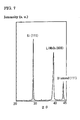
Fig. 7 shows an X-ray diffraction pattern for a Li(NbxTa1-x)O3 thin film
formed in Embodiment 5.
Fig. 8 shows an X-ray diffraction pattern for a Li(NbxTa1-x)O3 thin film
formed in Embodiment 5.
Fig. 9 illustrates an outline of a separate embodiment of a laser ablation
device of the present invention.
Fig. 10 illustrates an outline of a separate embodiment of a laser
ablation device of the present invention.
Fig. 11 diagrams characteristics of an SAW filter obtained in
Embodiment 6.
Fig. 12 illustrates an interdigitated electrode used for evaluation in the
present invention.
Best Mode for Carrying Out the Invention
The inventors found that among Li(NbxTa1-x)O3 (0 ≤ x ≤ 1) thin films that
are piezoelectric thin films, to form onto a polycrystalline diamond substrate
especially a piezoelectric thin film superior in piezoelectric characteristics,
laser ablation may be utilized to impart (110) orientation to the diamond in the
substrate, and the diamond substrate utilized superficially mirror-polished.
The (110) orientation of the diamond substrate may be, evaluating by the γ(110)
described earlier, 15% or more, more preferably 40% or more.
Diamond substrates that utilize a polycrystalline diamond fabricated by
a gas-phase synthesis technique are economical. The gas-phase synthesis of
diamond may be carried out under (110)-orienting conditions by a method
known to date, such as the microwave-plasma method or hot-filament method.
Although by varying the diamond-synthesizing conditions, (110)-oriented or
(100)-oriented diamond may be obtained, it was found that when diamond thin
films from these are utilized, compared to (110)-oriented diamond, the c-axis
orientation and the piezoelectric characteristics of the Li(NbxTa1-x)O3 thin film
are inferior. The substrate for when the diamond is gas-phase synthesized
may be anything that enables diamond to be synthesized, but Si wafers are
generally used. Following synthesis the diamond is superficially mirror-surface
processed using a diamond grindstone. Therein, the diamond surface
desirably is mirror-surface processed until its superficial smoothness Ry is 0.1
µm or less.
It is desirable that an amorphous layer 1 nm or more, 50 nm or less in
thickness be formed onto the diamond surface by the foregoing mirror-surface
process. Covering the polycrystalline-diamond surface with an amorphous
layer preferentially c-axis orients the Li(NbxTa1-xO3 thin film and allows it to
have optimal piezoelectric characteristics as a polycrystalline Li(NbxTa1-xO3
thin film. On the other hand, if the polycrystalline-diamond surface is not
covered with an amorphous layer, though the polycrystalline-diamond surface
is (110)-oriented, inasmuch as diamond crystals having other crystal azimuths
will be present, the crystal azimuth in which the Li(NbxTa1-x)O3 thin film is
grown will be subject to the influence of crystal azimuths apart from the (110)
of the diamond surface, making it difficult to obtain the favorable c-axis
orientation. For the foregoing mirror-surface process, in order that the
polycrystalline-diamond surface be covered with an amorphous layer, in the
mirror-surface processing using a diamond grindstone, controlling the amount
by which the diamond abrasive grains jut out from the diamond grindstone
surface is crucial. If the projection amount is large, the diamond abrasive
grains will polish tending to scratch the diamond surface of the polycrystalline
diamond substrate, which will make it hard to form the amorphous layer.
Some 2 µm is a suitable projection amount.
Utilized for the laser ablation, a laser is usable if 360 nm or less in
wavelength and 1 µsec or less in pulse duration. While ArF and F2 excimer
lasers would be lasers of this sort, it is desirable that laser-pulse energy density
be 1 J/cm2 or more, and a 248 nm-wavelength KrF excimer laser, which is
capable of activating oxygen, is most suitable. The preferable laser frequency
is some 1 to 50 Hz.
As to the laser ablation conditions, the temperature of the
polycrystalline diamond substrate may be 400°C or more, but if 1000°C or more,
the diamond will degenerate, and therefore 1000° C or less is preferable.
Likewise, an oxidizing gas consisting of oxygen, ozone, N2O, NO2, etc. is
desirable for the ambient, while a 0.1 to 100 Pa range is preferable for the
atmospheric pressure. If the atmospheric pressure is less than 0.1 Pa in
pressure, a piezoelectric thin film cannot be formed because the amount of
oxygen in the piezoelectric thin film is insufficient. Likewise, if the pressure
surpasses 100 Pa, the oxygen becomes excessive, whereupon the energy of the
vaporized Li(NbxTa1-x)O3 material drops due to collision with the ambient gas,
which therefore worsens the orientation of the Li(NbxTa1-x)O3 thin film. The
distance between the polycrystalline diamond substrate and the target is
suitably 10 nm or more, 1000 mm or less.
It was found that by the laser ablation method as above in order to form
onto a diamond substrate a Li(NbxTa1-x)O3 thin film whose orientation and
constituent proportions are favorable, during laser ablation the combination of
the temperature of the polycrystalline diamond substrate, and the atomic
constituent proportion Li/NbxTa1-x in the piezoelectric thin-film raw-material
target, is crucial.
In particular, in order to achieve the above-noted object of the present
invention, the combination of the diamond substrate temperature and the
target Li/NbxTa1-x atomic constituent proportion is set within the range
encompassed by points A, B, C, D and E in Fig. 6. Moreover, to obtain a
Li(NbxTa1-x)O3 thin film of good crystallinity and orientation, the range
encompassed by points F, G, H and I in Fig. 6 is satisfactory. When less than
400°C the Li(NbxTa1-x)O3 thin film becomes amorphous more readily without
crystallizing. 400°C or more, 1000°C or less is accordingly preferable.
Likewise, if the raw-material Li/NbxTa1-x proportion is less than 0.9,
crystallization not only of Li(NbxTa1-x)O3, but also of LiNb3O8 and like Li-deficient
phases proceeds, and the Li(NbxTa1-x)O3 thin film becomes amorphous
more readily. With larger Li/NbxTa1-x proportions, i.e., with more Li, an
amorphous layer is formed, but Li3NbO4 and like Li-excess phases are produced.
The raw-material target Li/NbxTa1-x proportion therefore is desirably 0.9 or
more, 1.5 or less. If the Li/NbxTa1-x proportion surpasses 1.5, when the
polycrystalline-diamond substrate temperature rises, the Li atoms vaporize
more readily, and the amount of Li in the thin film that is formed onto the
polycrystalline diamond substrate can be controlled to be within a 0.8 to 1.1
range. Nevertheless, 2.5 turns out to be the upper limit for the Li/NbxTa1-x
proportion, given equilibrium with the polycrystalline-diamond substrate
temperatures noted earlier. It is accordingly desirable that the
polycrystalline-diamond substrate temperature and the Li/NbxTa1-x proportion
be within the range as indicated in Fig. 6.
A Li(NbxTa1-x)O3 sintered body may be utilized for the raw-material
target. A sintered body in which to be the raw material Li2CO3 and Li2O are
admixed to adjust the composition may be utilized. The Li/NbxTa1-x
constituent proportion in the admixture preferably is within a range of 0.9 or
more, 2.5 or less.
The electrode for carrying out laser ablation while applying a bias
voltage may be anything that is electroconductive, but in terms of handling,
metal is preferable. Likewise, in order that polarization be carried out
uniformly, the area of the electrode should be at least be the same as the area of
the polycrystalline diamond substrate, or may be larger than that in area.
Although there is no particular upper limit, depending on the size of the device
used, an upper limit will naturally be determined.
Film-deposition of a Li(NbxTa1-x)O3 thin film utilizing a diamond
substrate, raw-material target, laser, and electrode as in the foregoing while
setting up an electric field in the diamond-substrate and electrode interval
makes it possible to form a Li(NbxTa1-x)O3 thin film superior in piezoelectric
characteristics. Inasmuch as forming a Li(NbxTa1-x)O3 thin film by a method
as above allows a polarization process to be conducted on the Li(NbxTa1-x)O3
thin film with an electric field smaller than the coercive electric field of single-crystal
Li(NbxTa1-x)O3, the piezoelectric characteristics will be superior.
This is because the Li(NbxTa1-x)O3 thin-film surface is in a quasi-steady
state during film deposition and inasmuch as the Li atoms, whose degree of
movement is high in crystallizing, travel following the electric field, a
sufficiently polarizing process may be performed with an electric field smaller
than that of the post-crystallization steady state.
The electric field is generated by installing a direct-current power source
in between the polycrystalline diamond substrate and the electrode, and
applying an electric potential to the electrode. To be polarization-enabling the
electric field the diamond-substrate and electrode interval should be 10 to 1000
V/cm. Polarization will not be effected at less than 10 V/cm. Likewise, in
excess of 1000 V/cm, because the electrode discharges, impurities are more
liable to become mixed into the forming Li(NbxTa1-x)O3 thin film, which ties in
at the same time with deterioration in film quality. Nevertheless, inasmuch
as electric discharge is liable to occur under a reduced-pressure atmosphere, in
order to suppress discharging and make the polarization process more efficient,
the electric field more preferably is 100 to 300 V/cm.
A Li(NbxTa1-x)O3 thin film formed onto a diamond substrate in the
foregoing way will be c-axis-oriented. Orientation assessment was made by
evaluating according to the X-ray rocking-pattern technique. Details of this
evaluation method are disclosed for example in Japanese Pub. Pat. App. No.
H08-32398. This method indicates that the smaller the standard deviation σ
of the measured rocking curve, the better the Li(NbxTa1-x)O3 orientation. The
σ value for Li(NbxTa1-x)O3 thin films in the present invention was 2° or less.
In addition, utilizing a diamond substrate on which a Li(NbxTa1-x)O3 thin
film obtained through the present invention was formed, a SAW filter was
prepared and its characteristics were evaluated, wherein a surface-acoustic
wave having a velocity of 10,000 m/s or more was present, and that the
piezoelectric characteristics of the obtained Li(NbxTa1-x)O3 thin film were
particularly outstanding was clearly evident.
Embodiment 1
Fig. 1 shows an outline of the device. The laser beam from an excimer
laser 1 is irradiated via a lens 2 and a window 3 onto a raw-material target 4,
instantaneously vaporizing the raw-material target to form a piezoelectric thin
film onto a diamond substrate 5. A sintered body (size: 20 mm × 5 mm) for
LiNbO3 to be the raw material was utilized as the raw-material target. The
Li/Nb constituent proportion in the target was made 1.0.
As to a polycrystalline diamond substrate, under (110)-orienting
conditions approximately 25 µm polycrystalline diamond was formed onto
single-crystal Si by a hot-filament gas-phase synthesis technique, after which
the diamond surface was mirror-surface processed utilizing a diamond
grindstone in which the diamond abrasive grains' projection amount was
controlled to be some 2 µm. The superficial smoothness Ry of the diamond
after being mirror-surfaced was 0.08 µm.
On observing the epi-surface of this diamond substrate (A) by the
transmission electron diffraction method, diffraction images were not apparent,
confirming that an amorphous layer had been formed. In the same way,
furthermore, a polycrystalline diamond substrate (B) in which the synthesized
diamond was mirror-surface processed utilizing a diamond grindstone in which
the diamond abrasive grains' projection amount was controlled to be 5 µm or
more was readied. On observing the surface of this diamond substrate (B)
likewise by the transmission electron diffraction method, diffraction images
were apparent, confirming that an amorphous layer had not been formed. The
superficial smoothness Ry of the diamond substrate (B), furthermore, was 0.08
µm.
Under an oxygen gas atmosphere LiNbO3 thin films were deposited onto
the two types of substrates described above by irradiating the laser beam from
a 248 nm-wavelength KrF excimer laser onto the sintered body. The output of
the laser utilized was 750 mJ, the laser-pulse energy density was J/cm2, and
the frequency was 5 Hz. The diamond substrate temperature was put at
500°C; the distance between the target and the diamond substrate, 80 mm; the
reaction pressure, 13 Pa; and the reaction time, 30 min.
X-ray diffraction patterns and rocking curves for the obtained LiNbO3
thin films are shown in Figs. 2 through 5. Figs. 2 and 3 are for wherein
diamond substrate (A) was utilized; Figs. 4 and 5 are for wherein diamond
substrate (B) was utilized. According to Figs. 2 and 3, the obtained LiNbO3
thin film was c-axis oriented, and the γc, being 100%, was exceedingly favorable.
Furthermore, with the σ value being 1.13°, it is evident that the orientation
was satisfactory. According to Figs. 4 and 5, in the case in which diamond
substrate (B) not having an amorphous layer was utilized, the LiNbO3 thin film
was c-axis oriented although (012) and (104) surfaces were apparent; the γc
therein was 69%. Likewise, with the σ value being 1.74°, the orientation was
better than that of LiNbO3 thin films obtained by conventional methods, but
was inferior to that for the instance in which a diamond substrate on which an
amorphous layer was formed was utilized. Here, the Li/Nb proportion in the
formed LiNbO3 thin film was 0.90 for diamond substrate (A), and was 0.89 for
diamond substrate (B).
Embodiment 2
The same device as in Embodiment 1 was utilized. A sintered body
(size: 20 mm × 5 mm) for an admixture of LiNbO3 and Li2CO3 to be the raw
material was utilized as the raw-material target. The Li/Nb constituent
proportion in the target was made 1.0.
As to polycrystalline diamond substrates, varying the orienting
conditions, polycrystalline diamond to 25 µm thickness was formed onto
single-crystal Si by a hot-filament gas-phase synthesis technique, after which
the diamond surfaces were mirror-surface processed. The γ(110) values
indicating superficial smoothness and orientation of the diamond after being
mirror-surfaced are shown in Table I. Here, the epi-surface of the diamond
substrates was observed by the transmission electron diffraction method
likewise as with Embodiment 1, confirming that amorphous layers had been
formed.
Utilizing raw-material target and polycrystalline diamond substrates as
in the above, and utilizing the same laser as in
Embodiment 1, under an oxygen
gas atmosphere a LiNbO
3 thin film was deposited onto the polycrystalline
diamond substrates. The laser ablation conditions were made the same
conditions as in
Embodiment 1. σ values measured by the X-ray diffraction
pattern technique, and thin-film Li/Nb proportions, for the formed LiNbO
3 thin
films are shown in Table I.
| | Diamond surface smoothness (µm) | γ(110) (%) | σ value (°) | Film constituent proportion |
| 1 | 0.07 | 61 | 1.22 | 0.87 |
| 2 | 0.10 | 22 | 1.74 | 0.91 |
| 3 | 0.10 | 5 | 2.15 | 0.86 |
As is evident from Table I, the larger the value of γ(110) indicating the
(110) orientation of the diamond substrate, the smaller the σ value for the
formed LiNbO3 thin film becomes, meaning that its c-axis orientation is
excellent.
Embodiment 3
The same device as in Embodiment 1 was utilized. A sintered body
(size: 20 mm × 5 mm) for an admixture of LiNbO3 and Li2CO3 to be the raw
material was utilized as the raw-material target. The Li/Nb constituent
proportion in the target was adjusted so as to make the compositions indicated
in Table II.
As to polycrystalline diamond substrates, polycrystalline diamond was
formed under the orienting conditions shown in Table II, and to the thicknesses
shown in Table II, onto single-crystal Si by a hot-filament gas-phase synthesis
technique, after which the diamond surfaces were mirror-surface processed.
The superficial smoothnesses of the diamond after being mirror-surfaced are
shown in Table II. Here, the epi-surface of the diamond substrates was
observed by the transmission electron diffraction method likewise as with
Embodiment 1, confirming that amorphous layers had been formed. Utilizing
a raw-material target and polycrystalline diamond substrates as in the above,
and utilizing the same laser as in
Embodiment 1, under an oxygen gas
atmosphere a LiNbO
3 thin film was deposited onto the polycrystalline diamond
substrates. The laser ablation conditions, as well as σ values measured by the
X-ray diffraction pattern technique, and film Li/Nb proportions, for the formed
LiNbO
3 thin films are shown in Table II.
Results of X-ray diffraction measuring on Nos. 4 and 5 made clear that
they were c-axis oriented. With regard to No. 6, micro-particles were
numerously apparent on the surface of the obtained thin film, and results of X-ray
diffraction measuring made clear that it was in an uncrystallized
amorphous form. Although in outward appearance thin film No. 7 quite
resembled thin film No. 4, with measuring by X-ray diffraction resulting in
strong peaks at (012) and (104) orientations, it was not c-axis oriented.
Although thin film No. 8 was c-axis oriented, with the σ value being 2.1° the
LiNbO3 orientation was not better than thin film No. 4 utilizing a (110)-oriented
polycrystalline diamond substrate.
Embodiment 4
The same device as in Embodiment 1 was utilized. A sintered body
(size: 20 mm × 5 mm) for LiTaO3 to be the raw material was utilized as the
raw-material target. Here, as to the Li/Ta constituent proportion in the No. 10
target, LiTaO3 and Li2CO3 were admixed and adjusted so as to make the
composition indicated in Table III.
As to polycrystalline diamond substrates, polycrystalline diamond was
formed under the orienting conditions shown in Table III, and to the
thicknesses shown in Table III, onto single-crystal Si by a hot-filament gas-phase
synthesis technique, after which the diamond surfaces were mirror-surface
processed. The superficial smoothnesses of the diamond after being
mirror-surfaced are shown in Table III. Here, the epi-surface of the diamond
substrates was observed by the transmission electron diffraction method
likewise as with
Embodiment 1, confirming that amorphous layers had been
formed. Utilizing a raw-material target and polycrystalline diamond
substrates as in the above, and utilizing the same laser as in
Embodiment 1,
under an oxygen gas atmosphere a LiTaO
3 thin film was deposited onto the
polycrystalline diamond substrates. The laser ablation conditions, and σ
values measured by the X-ray diffraction pattern technique for the formed
LiTaO
3 thin films, are shown in Table III.
An X-ray diffraction measurement was carried out on the LiTaO3 thin
film obtained in No. 9, wherein other than the peak that is natural to diamond,
a peak at 39.28° appeared. This corresponds to a Miller index (006) for LiTaO3,
which made it clear that the formed LiTaO3 thin film was c-axis oriented. Its
σ value being 1.13° demonstrates that the c-axis orientation was satisfactory.
Although No. 10, No. 11, and also No. 12 clearly turned out to be c-axis oriented,
with the σ value for No. 12 being 2.1° owing to it utilizing a (100)-oriented
polycrystalline diamond substrate, it turned out not to be better than No. 9,
which utilized a (110)-oriented polycrystalline diamond substrate. Microparticles
were numerously apparent on the surface of the No. 13 thin film, and
measuring by X-ray diffraction made clear that it was in an amorphous form.
Although in outward appearance thin film No. 14 quite resembled No. 9, in the
results from X-ray diffraction measurement, other than the peak that is
natural to diamond, peaks at 23.76°, 32.88° and 39.30° were apparent. These
correspond to Miller indices (012), (104) and (006) for the LiTaO3 thin film,
which demonstrated that it was not c-axis oriented.
Embodiment 5
The same device as in Embodiment 1 was utilized. A sintered body
(size: 20 mm × 5 mm) in which raw material 1 and raw material 2 set forth in
Table IV were admixed, adjusting so as to make the target constituent
proportion indicated in Table IV, to be the raw material was utilized as the
raw-material target. As to polycrystalline diamond substrates, under (110)-orienting
conditions approximately 25 µm polycrystalline diamond was formed
onto single-crystal Si by a hot-filament gas-phase synthesis technique, after
which the diamond surface was mirror-surface processed. The superficial
smoothness of the diamond after being mirror-surfaced was Ry 0.08 µm. Here,
the epi-surface of the diamond substrates was observed by the transmission
electron diffraction method likewise as with Embodiment 1, confirming that
amorphous layers had been formed.
Utilizing raw-material targets and polycrystalline diamond substrates
as in the above, and utilizing the same laser as in
Embodiment 1, under an
oxygen gas atmosphere a LiNbO
3 thin film was deposited onto the
polycrystalline diamond substrates. The laser ablation conditions, apart from
the substrate temperatures and reaction times, are the same as
Embodiment 1.
Diamond-substrate temperature conditions, and thin-film compositions
obtained by emission spectral analysis of the formed LiNbO
3 thin-films are
shown in Table IV. Here, the reaction time was 10 min.
| No. | Raw material 1 | Raw material 2 | Target constituent proportion | Substrate temperature (°C) | σ value (°) | Li/Nb proportion |
| 15 | LiNbO3 | Li2CO3 | 1.1 | 500 | 1.32 | 1.01 |
| 16 | LiNbO3 | Li2O | 1.2 | 550 | 1.44 | 1.02 |
| 17 | LiNbO3 | Li2CO3 | 1.6 | 650 | - | 1.09 |
| 18 | LiNbO3 | Li2CO3 | 2.5 | 500 | - | 1.66 |
An X-ray diffraction pattern for the thin film obtained in No. 15 is
illustrated in Fig. 7. From the figure it is evident that the obtained LiNbO3
thin film is single-phase LiNbO3 and c-axis oriented. On examining the
obtained thin-film composition under emission spectral analysis, the Li/Nb
proportion was 1.01, which means it was near the stoichiometric composition.
An X-ray diffraction analysis was done on the No. 16 thin film, wherein it was
single-phase LiNbO3. Furthermore, on examining the composition of the
obtained thin film under emission spectral analysis, the Li/Nb proportion was
1.02. An X-ray diffraction pattern for the thin film obtained in No. 17 is
illustrated in Fig. 8. From the figure it is evident that the obtained LiNbO3
thin film is single-phase LiNbO3, but that with a (104) peak apparent, its c-axis
orientation is not satisfactory. Furthermore, on examining composition of the
obtained thin film under emission spectral analysis, the Li/Nb proportion was
1.09. Results of measuring by X-ray diffraction the thin film obtained in No.
18 were that it was in an uncrystallized amorphous form. Likewise, from the
results of carrying out an emission spectral analysis it was evident that the
Li/Nb proportion, being1.66, deviated significantly from the stoichiometric
composition. It was understood that making the polycrystalline diamond
substrate and the Li/Nb proportion for the target be within the range shown in
Fig. 6 enables rendering a thin film whose orientation is superior―a formed
LiNbO3 thin film whose Li/Nb proportion will be 0.08 or more, 1.10 or less.
Embodiment 6
An outline of an embodiment of the present invention that involves
applying a bias voltage is illustrated in Fig. 9. An electrode 7 was arranged in
between the raw-material target 4 and the diamond substrate 5, in parallel
with the diamond substrate. A sintered body (size: 20 mm × 5 mm) for
LiNbO3 powder to be the raw material was utilized as the raw-material target.
The Li/Nb constituent proportion in the target was 1.0. The electrode utilized
was one in which tungsten wires 0.15 mm in diameter were strung vertically at
2 mm spacings and fixed to a stainless-steel frame. As to the diamond
substrate, under (110)-orienting conditions approximately 25 µm
polycrystalline diamond was formed onto single-crystal Si by a hot-filament
gas-phase synthesis technique, after which the diamond surface was mirror-surface
processed. The superficial smoothness of the diamond after being
mirror-surfaced was Ry 0.08 µm. Here, the epi-surface of the diamond
substrate was observed by the transmission electron diffraction method
likewise as with Embodiment 1, confirming that amorphous layers had been
formed. The diamond substrate and the electrode were disposed in parallel
with the raw-material target. Under an oxygen gas atmosphere, a LiNbO3
thin film was deposited onto the substrate by irradiating the laser beam from
the 248 nm-wavelength KrF excimer laser 1 via the lens 2 and the window 3
onto the sintered-body target.
The electrode potential was put at 140 V by a direct-current power
source 8, and the diamond-substrate potential put to 0 V (ground 9). The
distance between the electrode and the substrate was 6 mm, and the electric
field in the electrode and substrate interval was 233 V/cm. The substrate
temperature was put at 530°C, and the reaction time set to 6 min. Apart from
that, conditions were likewise as with Embodiment 1.
Synthesis of a LiNbO3 thin film onto the diamond substrate was carried
out under the foregoing conditions. the σ value for the obtained LiNbO3 thin
film was 1.27°, and the Li/Nb proportion was 0.84°. A 3.2 µm-pitch interdigital
transducer (abbreviated "IDT" hereinafter) as depicted in Fig. 12 was built by a
photolithographic process onto the formed LiNbO3 thin film. The utilizing the
IDT its SAW filter characteristics were evaluated, wherein it was evident that
frequency characteristics as in Fig. 11 were obtained, and that surface-acoustic
waves having a speed of 12,400 m/s were present. These facts indicate that
the piezoelectric characteristics of the obtained LiNbO3 thin film are excellent.
For comparison, a LiNbO3 thin film was formed under the same
conditions as with Embodiment 5, without setting up an electric field in the
electrode and substrate interval. An IDT was built on the formed LiNbO3 thin
film in the same manner as in Embodiment 5, and its SAW filter characteristics
were evaluated, wherein it was evident that SAW filter characteristics were not
obtained, meaning that a piezoelectrically poor LiNbO3 thin film had been
formed.
Embodiment 7
The same device, raw-material target, electrode, and diamond substrate
as with Embodiment 6 were utilized. Except for the electric potential between
the electrode and the substrate, the film-deposition conditions were made the
same as with Embodiment 1. An electric field of 233 V/cm was set up in the
electrode and substrate interval by making the electrode electric potential 0 V
(ground) and the electric potential on the diamond substrate -140 V. An IDT
was built, in the same manner as in Embodiment 6, on the LiNbO3 thin film
formed in this way, and its SAW filter characteristics were evaluated, wherein
it was evident that results likewise as with Embodiment 6 were obtained,
meaning that a LiNbO3 thin film of excellent piezoelectric characteristics had
been formed.
Embodiment 8
The same device, electrode, diamond substrate, and film-deposition
conditions as with Embodiment 6 were utilized. A sintered body in which
Li(Nb0.5Ta0.5)O3 powder was sintered was utilized for the raw-material target.
An IDT was built, in the same manner as in Embodiment 6, on the
Li(Nb0.5Ta0.5)O3 thin film formed in this way, and its SAW filter characteristics
were evaluated, wherein it was evident that results likewise as with
Embodiment 6 were obtained, meaning that a Li(Nb0.5Ta0.5)O3 thin film of
excellent piezoelectric characteristics had been formed.
Embodiment 9
The device illustrated in Fig. 10 was utilized. The diamond substrate 5
and an electrode 10 were arranged so as to be normal to a raw material target
13. With the layout being thus, inasmuch as particles that laser ablation
ejects from the target will not pass through the electrode, in-mixing into the
formed thin film of impurities such as electrode components may be lessened.
A sintered body (size: 20 mm × 5 mm) for LiNbO3 powder to be the raw
material was utilized as the raw-material target. The Li/Nb constituent
proportion in the target was 1.0. A stainless-steel sheet 1 mm thick was
utilized for the electrode. As to the diamond substrate, under (110)-orienting
conditions approximately 25 µm polycrystalline diamond was formed onto
single-crystal Si by a hot-filament gas-phase synthesis technique, after which
the diamond surface was mirror-surface processed. The superficial
smoothness of the diamond after being mirror-surfaced was Ry 0.08 µm. Here,
the epi-surface of the diamond substrate was observed by the transmission
electron diffraction method likewise as with Embodiment 1, confirming that
amorphous layers had been formed. Under an oxygen gas atmosphere, a
LiNbO3 thin film was deposited onto the diamond substrate by irradiating the
laser beam from the 248 nm-wavelength KrF excimer laser 1 via the lens 2 and
the window 3 onto the sintered-body target.
The electrode potential was put at 140 V by a direct-current power
source 8, and the diamond-substrate potential put to 0 V (ground 9). The
distance between the electrode and the substrate was 6 mm, and the electric
field in the electrode and substrate interval was 233 V/cm. The substrate
temperature was put at 530°C, and the reaction time set to 8 min. Apart from
that, conditions were likewise as with Embodiment 1. It should be understood
that the distance between the target and the diamond substrate in this case is
given by the distance between the target surface and the center of the diamond
substrate.
An IDT was built, in the same manner as in Embodiment 6, on the
LiNbO3 thin film formed in this way, and its SAW filter characteristics were
evaluated, wherein it was evident that results likewise as with Embodiment 6
were obtained, meaning that a LiNbO3 thin film of excellent piezoelectric
characteristics had been formed.
Industrial Applicability
In terms of the present invention as in the foregoing, specifying as (110)
the orientation of a gas-phase synthesized polycrystalline diamond per se and
mirror-surface processing the diamond surface, enables a favorably c-axis
oriented Li(NbxTa1-x)O3 thin film to be formed onto the diamond utilizing a
laser ablation technique. The formed Li(NbxTa1-x)O3 thin films exhibit
favorable c-axis orientation not present to date. Likewise, if the gas-phase
synthesized polycrystalline diamond is superficially covered with an
amorphous layer the formed Li(NbxTa1-x)O3 thin films will manifest still better
piezoelectric characteristics. Likewise, forming under an electric field a
Li(NbxTa1-x)O3 thin film onto the diamond substrate enables a Li(NbxTa1-x)O3 (0
≤ x ≤ 1) thin film whose piezoelectric characteristics are more outstanding to be
obtained. Most favorable are the piezoelectric characteristics of a
Li(NbxTa1-x)O3 thin film formed by a laser ablation technique under an electric
field onto a (110)-oriented gas-phase synthesized polycrystalline diamond
substrate superficially covered with an amorphous layer. Surface-acoustic
wave devices having high propagation speeds may be fabricated utilizing a
composite substrate on which this sort of piezoelectrically outstanding
Li(NbxTa1-x)O3 (0 ≤ x ≤ 1) thin film formed onto a diamond substrate is built.