EP1375697A1 - Laminated film and method of forming film - Google Patents
Laminated film and method of forming film Download PDFInfo
- Publication number
- EP1375697A1 EP1375697A1 EP01273954A EP01273954A EP1375697A1 EP 1375697 A1 EP1375697 A1 EP 1375697A1 EP 01273954 A EP01273954 A EP 01273954A EP 01273954 A EP01273954 A EP 01273954A EP 1375697 A1 EP1375697 A1 EP 1375697A1
- Authority
- EP
- European Patent Office
- Prior art keywords
- film
- substrate
- forming
- oxide
- deposition method
- Prior art date
- Legal status (The legal status is an assumption and is not a legal conclusion. Google has not performed a legal analysis and makes no representation as to the accuracy of the status listed.)
- Withdrawn
Links
- 0 CC(C1(*)*(*C=C)CCC1)=C Chemical compound CC(C1(*)*(*C=C)CCC1)=C 0.000 description 1
Images


Classifications
-
- C—CHEMISTRY; METALLURGY
- C23—COATING METALLIC MATERIAL; COATING MATERIAL WITH METALLIC MATERIAL; CHEMICAL SURFACE TREATMENT; DIFFUSION TREATMENT OF METALLIC MATERIAL; COATING BY VACUUM EVAPORATION, BY SPUTTERING, BY ION IMPLANTATION OR BY CHEMICAL VAPOUR DEPOSITION, IN GENERAL; INHIBITING CORROSION OF METALLIC MATERIAL OR INCRUSTATION IN GENERAL
- C23C—COATING METALLIC MATERIAL; COATING MATERIAL WITH METALLIC MATERIAL; SURFACE TREATMENT OF METALLIC MATERIAL BY DIFFUSION INTO THE SURFACE, BY CHEMICAL CONVERSION OR SUBSTITUTION; COATING BY VACUUM EVAPORATION, BY SPUTTERING, BY ION IMPLANTATION OR BY CHEMICAL VAPOUR DEPOSITION, IN GENERAL
- C23C14/00—Coating by vacuum evaporation, by sputtering or by ion implantation of the coating forming material
- C23C14/22—Coating by vacuum evaporation, by sputtering or by ion implantation of the coating forming material characterised by the process of coating
- C23C14/24—Vacuum evaporation
-
- C—CHEMISTRY; METALLURGY
- C23—COATING METALLIC MATERIAL; COATING MATERIAL WITH METALLIC MATERIAL; CHEMICAL SURFACE TREATMENT; DIFFUSION TREATMENT OF METALLIC MATERIAL; COATING BY VACUUM EVAPORATION, BY SPUTTERING, BY ION IMPLANTATION OR BY CHEMICAL VAPOUR DEPOSITION, IN GENERAL; INHIBITING CORROSION OF METALLIC MATERIAL OR INCRUSTATION IN GENERAL
- C23C—COATING METALLIC MATERIAL; COATING MATERIAL WITH METALLIC MATERIAL; SURFACE TREATMENT OF METALLIC MATERIAL BY DIFFUSION INTO THE SURFACE, BY CHEMICAL CONVERSION OR SUBSTITUTION; COATING BY VACUUM EVAPORATION, BY SPUTTERING, BY ION IMPLANTATION OR BY CHEMICAL VAPOUR DEPOSITION, IN GENERAL
- C23C14/00—Coating by vacuum evaporation, by sputtering or by ion implantation of the coating forming material
- C23C14/22—Coating by vacuum evaporation, by sputtering or by ion implantation of the coating forming material characterised by the process of coating
- C23C14/225—Oblique incidence of vaporised material on substrate
-
- C—CHEMISTRY; METALLURGY
- C23—COATING METALLIC MATERIAL; COATING MATERIAL WITH METALLIC MATERIAL; CHEMICAL SURFACE TREATMENT; DIFFUSION TREATMENT OF METALLIC MATERIAL; COATING BY VACUUM EVAPORATION, BY SPUTTERING, BY ION IMPLANTATION OR BY CHEMICAL VAPOUR DEPOSITION, IN GENERAL; INHIBITING CORROSION OF METALLIC MATERIAL OR INCRUSTATION IN GENERAL
- C23C—COATING METALLIC MATERIAL; COATING MATERIAL WITH METALLIC MATERIAL; SURFACE TREATMENT OF METALLIC MATERIAL BY DIFFUSION INTO THE SURFACE, BY CHEMICAL CONVERSION OR SUBSTITUTION; COATING BY VACUUM EVAPORATION, BY SPUTTERING, BY ION IMPLANTATION OR BY CHEMICAL VAPOUR DEPOSITION, IN GENERAL
- C23C14/00—Coating by vacuum evaporation, by sputtering or by ion implantation of the coating forming material
- C23C14/22—Coating by vacuum evaporation, by sputtering or by ion implantation of the coating forming material characterised by the process of coating
- C23C14/24—Vacuum evaporation
- C23C14/28—Vacuum evaporation by wave energy or particle radiation
-
- C—CHEMISTRY; METALLURGY
- C30—CRYSTAL GROWTH
- C30B—SINGLE-CRYSTAL GROWTH; UNIDIRECTIONAL SOLIDIFICATION OF EUTECTIC MATERIAL OR UNIDIRECTIONAL DEMIXING OF EUTECTOID MATERIAL; REFINING BY ZONE-MELTING OF MATERIAL; PRODUCTION OF A HOMOGENEOUS POLYCRYSTALLINE MATERIAL WITH DEFINED STRUCTURE; SINGLE CRYSTALS OR HOMOGENEOUS POLYCRYSTALLINE MATERIAL WITH DEFINED STRUCTURE; AFTER-TREATMENT OF SINGLE CRYSTALS OR A HOMOGENEOUS POLYCRYSTALLINE MATERIAL WITH DEFINED STRUCTURE; APPARATUS THEREFOR
- C30B23/00—Single-crystal growth by condensing evaporated or sublimed materials
- C30B23/02—Epitaxial-layer growth
-
- C—CHEMISTRY; METALLURGY
- C30—CRYSTAL GROWTH
- C30B—SINGLE-CRYSTAL GROWTH; UNIDIRECTIONAL SOLIDIFICATION OF EUTECTIC MATERIAL OR UNIDIRECTIONAL DEMIXING OF EUTECTOID MATERIAL; REFINING BY ZONE-MELTING OF MATERIAL; PRODUCTION OF A HOMOGENEOUS POLYCRYSTALLINE MATERIAL WITH DEFINED STRUCTURE; SINGLE CRYSTALS OR HOMOGENEOUS POLYCRYSTALLINE MATERIAL WITH DEFINED STRUCTURE; AFTER-TREATMENT OF SINGLE CRYSTALS OR A HOMOGENEOUS POLYCRYSTALLINE MATERIAL WITH DEFINED STRUCTURE; APPARATUS THEREFOR
- C30B29/00—Single crystals or homogeneous polycrystalline material with defined structure characterised by the material or by their shape
- C30B29/10—Inorganic compounds or compositions
- C30B29/16—Oxides
-
- C—CHEMISTRY; METALLURGY
- C30—CRYSTAL GROWTH
- C30B—SINGLE-CRYSTAL GROWTH; UNIDIRECTIONAL SOLIDIFICATION OF EUTECTIC MATERIAL OR UNIDIRECTIONAL DEMIXING OF EUTECTOID MATERIAL; REFINING BY ZONE-MELTING OF MATERIAL; PRODUCTION OF A HOMOGENEOUS POLYCRYSTALLINE MATERIAL WITH DEFINED STRUCTURE; SINGLE CRYSTALS OR HOMOGENEOUS POLYCRYSTALLINE MATERIAL WITH DEFINED STRUCTURE; AFTER-TREATMENT OF SINGLE CRYSTALS OR A HOMOGENEOUS POLYCRYSTALLINE MATERIAL WITH DEFINED STRUCTURE; APPARATUS THEREFOR
- C30B29/00—Single crystals or homogeneous polycrystalline material with defined structure characterised by the material or by their shape
- C30B29/10—Inorganic compounds or compositions
- C30B29/16—Oxides
- C30B29/22—Complex oxides
-
- C—CHEMISTRY; METALLURGY
- C30—CRYSTAL GROWTH
- C30B—SINGLE-CRYSTAL GROWTH; UNIDIRECTIONAL SOLIDIFICATION OF EUTECTIC MATERIAL OR UNIDIRECTIONAL DEMIXING OF EUTECTOID MATERIAL; REFINING BY ZONE-MELTING OF MATERIAL; PRODUCTION OF A HOMOGENEOUS POLYCRYSTALLINE MATERIAL WITH DEFINED STRUCTURE; SINGLE CRYSTALS OR HOMOGENEOUS POLYCRYSTALLINE MATERIAL WITH DEFINED STRUCTURE; AFTER-TREATMENT OF SINGLE CRYSTALS OR A HOMOGENEOUS POLYCRYSTALLINE MATERIAL WITH DEFINED STRUCTURE; APPARATUS THEREFOR
- C30B29/00—Single crystals or homogeneous polycrystalline material with defined structure characterised by the material or by their shape
- C30B29/10—Inorganic compounds or compositions
- C30B29/16—Oxides
- C30B29/22—Complex oxides
- C30B29/225—Complex oxides based on rare earth copper oxides, e.g. high T-superconductors
-
- H—ELECTRICITY
- H10—SEMICONDUCTOR DEVICES; ELECTRIC SOLID-STATE DEVICES NOT OTHERWISE PROVIDED FOR
- H10N—ELECTRIC SOLID-STATE DEVICES NOT OTHERWISE PROVIDED FOR
- H10N60/00—Superconducting devices
- H10N60/01—Manufacture or treatment
- H10N60/0268—Manufacture or treatment of devices comprising copper oxide
- H10N60/0296—Processes for depositing or forming copper oxide superconductor layers
- H10N60/0576—Processes for depositing or forming copper oxide superconductor layers characterised by the substrate
- H10N60/0632—Intermediate layers, e.g. for growth control
-
- Y—GENERAL TAGGING OF NEW TECHNOLOGICAL DEVELOPMENTS; GENERAL TAGGING OF CROSS-SECTIONAL TECHNOLOGIES SPANNING OVER SEVERAL SECTIONS OF THE IPC; TECHNICAL SUBJECTS COVERED BY FORMER USPC CROSS-REFERENCE ART COLLECTIONS [XRACs] AND DIGESTS
- Y10—TECHNICAL SUBJECTS COVERED BY FORMER USPC
- Y10T—TECHNICAL SUBJECTS COVERED BY FORMER US CLASSIFICATION
- Y10T428/00—Stock material or miscellaneous articles
- Y10T428/12—All metal or with adjacent metals
- Y10T428/12493—Composite; i.e., plural, adjacent, spatially distinct metal components [e.g., layers, joint, etc.]
Definitions
- the present invention relates to a stacked film and a deposition method, and more particularly to a method of depositing a stacked film as an intermediate layer where an oxide superconducting layer is formed with the intermediate layer interposed on a prescribed substrate.
- Japanese Patent Laying-Open No. 7-291626 describes a method of depositing an intermediate layer where an oxide superconducting layer is formed with the intermediate layer interposed on a substrate.
- an intermediate layer is formed by a laser ablation method in which a target material is irradiated with laser light and a substance scattered from the target material is evaporated onto a substrate.
- a film having a particular crystal axis approximately parallel to the normal line direction to the substrate is formed by depositing the intermediate layer with the substrate inclined at a prescribed angle with respect to the target material.
- a superconducting layer formed thereon is also oriented, resulting in an excellent superconducting characteristic.
- the distance between one end of the substrate and the target material is relatively large while the distance between the other end of the substrate and the target material is relatively small.
- the film thickness of the intermediate layer is reduced on the one end side at a long distance from the target material while the film thickness of the intermediate layer is increased at the other end side at a short distance from the target material. The film thickness of the intermediate layer thus varies greatly.
- the film thickness of the intermediate layer is correlated with the orientation of the intermediate layer. As the film thickness of the intermediate layer is increased, the orientation is improved. Therefore, the variations in film thickness result in variations in orientation. As a result, the superconducting layer formed on the intermediate layer varies in orientation, thereby preventing an excellent superconducting characteristic.
- the film thickness of the intermediate layer also affects the surface coarseness of the intermediate layer. As the film thickness of the intermediate layer is increased, the surface coarseness is increased. Since the variations in the film thickness of the intermediate layer result in variations in surface coarseness, the superconducting layer formed thereon varies in orientation. This also prevents an excellent superconducting characteristic.
- the present invention is therefore made to solve the aforementioned problem.
- An object of the present invention is to provide a stacked film with fewer variations in film thickness and a deposition method thereof.
- Another object of the present invention is to provide a stacked film having a particular crystal orientation being parallel to a normal line to a substrate, and a deposition method.
- a deposition material is scattered from a target material surface, and the scattered deposition material is grown on a substrate surface to form a film.
- the deposition method includes the following steps:
- the first film is formed in the first state where the distance between the one end of the substrate and the target material is relatively small and the distance between the other end of the substrate and the target material is relatively large, so that the first film has a thickness increased at the one end side of the substrate and a thickness reduced at the other end side of the substrate.
- the second film is thereafter formed on the first film in the second state where the distance between the one end of the substrate and the target material is relatively large and the distance between the other end of the substrate and the target material is relatively small, so that the second film has a thickness reduced at the one end side of the substrate and a thickness increased at the other end side of the substrate.
- the film thickness is approximately equal at the one end side and the other end side of the substrate.
- the deposition material is supplied from the one end side of the substrate as the distance between the one end side of the substrate and the target is relatively short.
- the deposition material is supplied from the other end side of the substrate as the distance between the other end of the substrate and the target material is short.
- the deposition material is supplied from the both sides of the substrate, and a particular orientation of the film can be approximately parallel to the normal line direction to the substrate.
- the deposition method further includes a step of forming a superconducting layer on the second film.
- the deposition method further includes steps of positioning the substrate into a third state where the surface of the substrate is opposed to the surface of the target material, and forming a third film on the second film in the third state.
- the step of positioning the substrate into a third state includes a step of positioning the substrate such that the surface of the substrate is opposed approximately parallel to the surface of the target material.
- the deposition method further includes a step of forming a superconducting layer on the third film.
- the step of forming a superconducting layer includes a step of forming a superconducting layer including the following elements: at least one kind of element selected from the group consisting of yttrium (Y), holmium (Ho), samarium (Sm), lutetium (Lu), ytterbium (Yb), thulium (Tm), erbium (Er), dysprosium (Dy), gadolinium (Gd), europium (Eu), lanthanum (La) and neodymium (Nd); barium (Ba); copper (Cu); and oxygen (O), approximately at a ratio of 1:2:3:y (y is a number equal to or greater than 6).
- Y yttrium
- Ho holmium
- Sm samarium
- Lu lutetium
- Yb thulium
- Er erbium
- Dy dysprosium
- Gd gadolinium
- Eu europium
- La
- the step of forming a superconducting layer includes a step of forming a plurality of superconducting layers.
- the step of forming a plurality of superconducting layers includes a step of forming a plurality of superconducting layers having different compositions.
- the step of forming a superconducting layer includes forming a superconducting layer by any of ion beam sputtering (IBS), sputtering, thermal co-evaporation, MOD (Metal Organic Decomposition), MBE (Molecular Beam Epitaxy), MOCVD (Metal Organic Chemical Vapor Deposition), electron beam evaporation, and laser ablation.
- IBS ion beam sputtering
- sputtering thermal co-evaporation
- MOD Metal Organic Decomposition
- MBE Molecular Beam Epitaxy
- MOCVD Metal Organic Chemical Vapor Deposition
- electron beam evaporation and laser ablation.
- the target material is oxide.
- the target material includes at least one kind selected from the group consisting of strontium titanium oxide (SrTiO 3 ), magnesium oxide (MgO), zirconium oxide (ZrO 2 ), hafnium oxide (HfO 2 ), praseodymium oxide (PrO 2 ), zirconium gadolinium oxide (Zr 2 Gd 2 O 7 ), zirconium samarium oxide (Zr 2 Sm 2 O 7 ), zirconium lanthanum oxide (Zr 2 La 2 O 7 ), samarium oxide (Sm 2 O 3 ), barium zirconium oxide (BaZrO 3 ), neodymium gallium oxide (NdGaO 3 ), yttria stabilized zirconia (YSZ), yttrium oxide (Y 2 O 3 ), cerium oxide (CeO 2 ), ytterbium oxide (Yb 2 O 3 ), and holmium oxide (Ho 2 O 3 ).
- an amount of cation evaporated per unit area is approximately equal in moles in the step of forming a first film and the step of forming a second film.
- the step of forming a first film and the step of forming a second film includes forming a film by electron beam evaporation, laser ablation, sputtering, or a combination thereof.
- the substrate is a metal tape having flexibility, and a direction from the one end to the other end is approximately orthogonal to a longitudinal direction of the metal tape.
- the substrate includes at least one kind selected from the group consisting of silver, silver alloy, nickel, nickel alloy and stainless steel.
- the substrate includes a plurality of layers, and each of a plurality of layers includes at least one kind selected from the group consisting of silver, silver alloy, nickel, nickel alloy, and stainless steel.
- the deposition method further includes a step of repeating the step of forming a first film and the step of forming a second film alternately multiple times.
- the stacked film in accordance with the present invention is manufactured in one of the aforementioned methods.
- the stacked film has a multilayered structure that allows distortion to be distributed as compared with a single layer structure.
- the interface between films is inclined to the substrate surface, it is possible to design the direction in which the distortion escapes.
- the present invention is therefore advantageous over the conventional technique in that it has a degree of freedom in its structure design where the wire material itself disperses the distortion.
- the multilayer allows the number of interfaces between films to be controlled, the heat resistance and electric resistance can be controlled.
- the interface is inclined to the substrate surface, the area of the interface can be controlled and the heat resistance and electric resistance can thus be varied. This additional factor to control a physical property value as a structure increases the degree of freedom in material design.
- the present invention is advantageous over the conventional technique as the control of the heat resistance and electric resistance is important.
- Fig. 1 is a side view of a deposition device used in a first example of the present invention.
- Fig. 2 is a front view of the deposition device as seen from the direction indicated by arrow II in Fig. 1.
- a deposition device 1 has a vacuum chamber 10, a support rod 11 provided in vacuum chamber 10, a target 12 attached to support rod 11, and a laser oscillation device 20 externally irradiating target 12 with laser.
- a substrate 100 is positioned at a position away from target 12.
- Substrate 100 has a main surface 100a, one end 100f, and the other end 100e.
- a normal line 100b to main surface 100a forms a prescribed angle ⁇ with a normal line 12b to a main surface 12a of target 12.
- Support rod 11 is rotated to rotate target 12 in a direction indicated by arrow R.
- Fig. 3 is a side view of the deposition device shown to illustrate a step of depositing a first film.
- Fig. 4 is a front view of the deposition device as seen from the direction indicated by arrow IV in Fig. 3.
- the vacuum chamber was filled with argon gas.
- Substrate 100 was arranged such that the distance from the central portion of target 12 to the central portion of substrate 100 was 50 mm.
- Substrate 100 was heated to a temperature of 650°C by a heater.
- Substrate 100 has a width of 10 mm, a length of 200 mm and a thickness of 0.1 mm, and is shape like a longitudinally extending tape.
- Substrate 100 is formed of nickel alloy.
- Target 12 was irradiated with KrF excimer laser of a wavelength of 248 nm from the direction indicated by arrow 21.
- the laser energy density was 2J/cm 2 and the frequency was 150 Hz.
- Target 12 was rotated in the direction indicated by arrow R.
- target 12 emitted laser plume (luminous seed) 13.
- Substrate 100 was longitudinally transferred in the direction indicated by arrow 102 at a speed of 7 mm/min.
- a first film was deposited with substrate 100 continuously passed through laser plume 13.
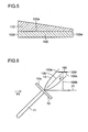
- Fig. 5 is a cross sectional view of the substrate on which the first film is deposited. Referring to Fig. 5, a first film 110 was deposited on main surface 100a of substrate 100. The thickness of first film 110 was relatively large in the vicinity of one end 100f and was relatively small in the vicinity of the other end 100e.
- Fig. 6 is a side view of the deposition device shown to illustrate a step of depositing a second film.
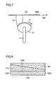
- Fig. 7 is a front view of the deposition device as seen from the direction indicated by arrow VII in Fig. 6.
- substrate 100 was arranged in a second state where the distance between one end 100f of substrate 100 and target 12 was relatively large and the distance between the other end 100e of substrate 100 and target 12 was relatively small.
- Normal line 100b to main surface 100a of substrate 100 formed an angle of approximately 45° with normal line 12b to main surface 12a of target 12.
- target 12 was irradiated with laser from the direction indicated by arrow 21 under the same conditions as the step shown in Figs. 3 and 4.
- Laser plume 13 was thereby generated to deposit the second film on substrate 100.
- Fig. 8 is a cross sectional view of the substrate on which the second film is deposited.
- first film 110 is deposited on substrate 100
- second film 120 is deposited on first film 110.
- the thickness of second film 120 is smaller at the one end 100f side of substrate 100 and the thickness of second film 120 is larger at the other end 100e side. It is noted that first film 110 and second film 120 have the same composition. In combination of first film 110 and second film 120, the film thickness is approximately equal at the one end 100f side and the other end 100e side.
- First film 110 and second film 120 are YSZ thin film serving as an intermediate layer.
- the resultant YSZ thin film was evaluated by an X-ray diffraction method, and a strong peak indicating orientation of [200] plane was observed. As a result, it was found that [200] plane was approximately parallel to main surface 100a of substrate 100 and was strongly oriented.
- ⁇ ' shift the shift between normal line 100b to main surface 100a of substrate 100 and ⁇ 200> direction of YSZ thin film ( ⁇ ' shift) was evaluated by the X-ray pole figure measurement.
- the ⁇ ' shift was 32°.
- the film thickness distribution of YSZ thin film was examined in the direction from one end 100f to the other end 100e of substrate 100 of YSZ thin film, to find that the film thicknesses at positions 3 mm, 5 mm and 7 mm away from one end 100f were 2.1 ⁇ m, 2.2 ⁇ m and 2.1 ⁇ m, respectively.
- the variation of the film thickness in this range was 0.1 ⁇ m.
- a thin film of yttrium oxide (Y 2 O 3 ) was formed as a third film on YSZ thin film produced in the first example.
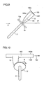
- Fig. 9 is a side view of the deposition device shown to illustrate a step of depositing a third film.
- Fig. 10 is a front view of the deposition device as seen from the direction indicated by X in Fig. 9.. Referring to Figs. 9 and 10, target 12 made of yttrium oxide was prepared, and deposition was performed using deposition device 1 while target 12 and substrate 100 were arranged parallel to each other.
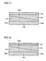
- Fig. 11 is a cross sectional view of the substrate on which the third film is formed.
- first film 110 is formed on main surface 100a of substrate 100
- second film 120 is formed on first film 110
- third film 130 is formed on second film 120.
- Third film 130 is an yttrium oxide thin film.
- the resultant yttrium oxide thin film was evaluated by the X-ray diffraction method, and a strong peak indicating orientation of [400] plane was observed. As a result, it was found that [400] plane was strongly oriented approximately parallel to main surface 100a.
- the film thickness distribution of the composite thin film formed of the yttria stabilized zirconia thin film and the yttrium oxide film was examined.
- the film thicknesses at positions 3 mm, 5 mm and 7 mm away from one end 100f of substrate 100 were 2.1 ⁇ m, 2.2 ⁇ m and 2.1 ⁇ m, respectively.
- the variation of the film thickness in this range was 0.1 ⁇ m.
- a cerium oxide (CeO 2 ) thin film was formed as the third film of the second example.
- cerium oxide was used as a target.
- the other conditions were set as similar to the second example.
- the resultant cerium oxide thin film was measured by the X-ray diffraction method, and a strong peak indicating the orientation of [200] plane was observed. As a result, it was found that [200] plane of the cerium oxide thin film was strongly oriented approximately parallel to main surface 100a of substrate 100.
- the film thickness distribution of the composite thin film made of the yttria stabilized zirconia thin film and the cerium oxide thin film was examined.
- the film thicknesses at positions 3 mm, 5 mm and 7 mm away from one end 100f of substrate 100 were 2.1 ⁇ m, 2.2 ⁇ m and 2.2 ⁇ m, respectively.
- the variation of the film thickness in this range was 0.1 ⁇ m.
- an ytterbium oxide (Yb 2 O 3 ) thin film was formed as the third film. Therefore, a target of ytterbium oxide was used as a target in the third deposition.
- the other conditions were set similar to the second example.
- the resultant ytterbium oxide thin film was measured by the X-ray diffraction method, and a strong peak indicating orientation of ⁇ 400 ⁇ plane was observed. As a result, it was found that ⁇ 400 ⁇ plane was strongly oriented approximately parallel to main surface 100a of substrate 100.
- the film thickness distribution of the composite thin film formed of the yttria stabilized zirconia thin film and the ytterbium oxide thin film was examined.
- the film thicknesses at positions 3 mm, 5 mm and 7 mm away from one end 100f of substrate 100 were 2.1 ⁇ m, 2.2 ⁇ m and 2.1 ⁇ m, respectively.
- the variation of the film thickness in this range was 0.1 ⁇ m.
- a holmium oxide (Ho 2 O 3 ) thin film was formed as the third film in the second example. Therefore, holmium oxide was used as a target.
- the other conditions were set similar to the second example.
- the resultant holmium oxide thin film was evaluated by the X-ray diffraction method, and a strong peak indicating orientation of ⁇ 400 ⁇ plane was observed. As a result, it was found that ⁇ 400 ⁇ plane was strongly oriented approximately parallel to main surface 100a of substrate 100.
- the film thickness distribution of the composite thin film formed of the yttria stabilized zirconia thin film and the holmium oxide thin film was examined.
- the film thicknesses at positions 3 mm, 5 mm and 7 mm away from one end 100f of substrate 100 were 2.1 ⁇ m, 2.2 ⁇ m and 2.1 ⁇ m, respectively.
- the variation of the film thickness in this range was 0.1 ⁇ m.
- an yttria stabilized zirconia thin film was formed only in the first state where the distance between one end 100f of substrate 100 and target 12 was relatively small and the distance between the other end 100e and target 12 was relatively large, as shown in Figs. 3 and 4 in the first example.
- the resultant yttria stabilized zirconia thin film was evaluated by the X-ray diffraction method, and a strong peak indicating orientation of ⁇ 200 ⁇ plane was observed. As a result, it was found that ⁇ 200 ⁇ plane was strongly oriented approximately parallel to main surface 100a of substrate 100.
- the film thickness distribution of the yttria stabilized zirconia thin film was examined.
- the film thicknesses at positions 3 mm, 5 mm and 7 mm away from one end 100f of substrate 100 were 1.7 ⁇ m, 2.1 ⁇ m and 2.6 ⁇ m, respectively.
- the variation of the film thickness in this range was 0.9 ⁇ m.
- the comparative example is characterized by deposition with the substrate being inclined.
- This deposition method is called ISD (Inclined Substrate Deposition).
- the first to fifth examples are characterized by deposition by ISD followed by deposition with the substrate inclined to the opposite direction. This deposition method is called RISD (Reverse ISD).
- RISD Reverse ISD
- a third deposition is performed with the target and the substrate arranged parallel to each other after the deposition by ISD.
- the deposition method in this arrangement is called parallel deposition.
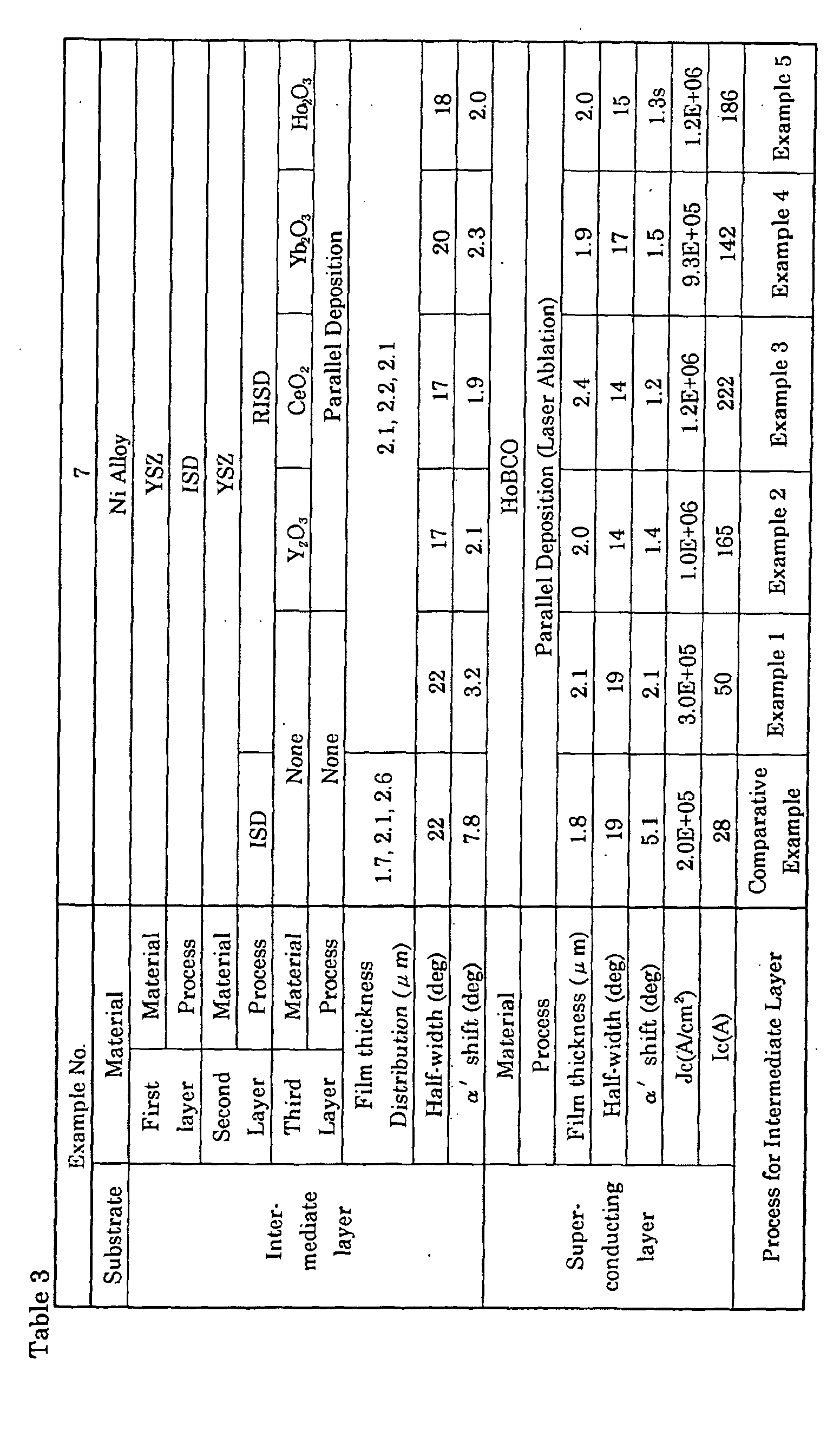
- Table 1 The results obtained from the first to fifth examples and the comparative example are shown in Table 1.
- a superconducting layer was deposited on the substrate fabricated in the comparative example and the first to fifth examples.
- Sintered YBa 2 Cu 3 O y (y is approximately 7) was used as a target of a superconducting material.
- y is roughly 6-7 and an oxygen amount varies with manufacturing conditions of the target.
- y is preferably as close to 7 as possible. In the following, this material will be abbreviated as YBCO for the sake of convenience.
- a substrate having the thin film fabricated in the comparative example and the first to fifth examples was positioned at a distance of 50 mm away from the target.
- the temperature of the substrate was set at 700°C by a heater.
- the pressure was 13Pa (0.10 Torr) in an oxygen gas atmosphere.
- the target was irradiated with laser under the conditions of a laser energy density of 20J/cm 3 and a frequency of 20Hz using KrF excimer laser of a wavelength of 248 nm.
- the target and the substrate were arranged to be parallel to each other.
- the target When the target was irradiated with laser light, the target emitted a luminous seed (a laser plume).
- the deposition was performed in such a manner that the substrate was longitudinally transferred at a speed of 3.3 mm/min and the substrate was continuously passed through the laser plume.
- the temperature of the substrate was gradually cooled from 700°C to the room temperature while the conditions of the pressure within the chamber at 13Pa (0.10 Torr) were maintained.
- Fig. 12 is a cross sectional view of the superconducting layer formed on the second film of the first example. Referring to Fig. 12, first film 110 is formed on substrate 100, second film 120 is formed on first film 110, and a superconducting layer 140 is formed on second film 120.
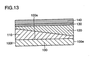
- Fig. 13 is a cross sectional view of the superconducting layer formed on the third film of the second to fifth examples.
- first film 110 is formed on substrate 100.
- Second film 120 is formed on first film 110.
- Third film 130 is formed on second film 120.
- Superconducting layer 140 is formed on third film 130.
- Critical current Ic and critical current density Jc were measured in liquid nitrogen of a temperature 77K in a self-magnetic field by a dc four-terminal method.
- the in-plane orientation of YBCO was evaluated with the half-width of ⁇ scan of ⁇ 103 ⁇ plane in the X-ray pole figure measurement.
- a superconducting layer was deposited on the substrate fabricated in the comparative example and the first to fifth examples.
- Sintered HoBa 2 Cu 3 O y (y is approximately 7) was used as a target of a superconducting material.
- y is roughly 6-7 and an oxygen amount varies with the manufacturing conditions of the target.
- y is preferably as close to 7 as possible. In the following, this material will be abbreviated as HoBCO for the sake of convenience.
- a superconducting layer of HoBCO thin film was formed on the substrate on which a thin film was fabricated in the comparative example and the first to fifth examples, under the similar conditions as the sixth example.
- a film of silver was produced on this superconducting layer under the similar conditions as the sixth example, and thereafter annealing was performed.
- the target and the substrate may make an acute angle.
- a superconducting layer may be formed including the following elements: at least one kind of element selected from the group consisting of yttrium (Y), holmium (Ho), samarium (Sm), lutetium (Lu), ytterbium (Yb), thulium (Tm), erbium (Er), dysprosium (Dy), gadolinium (Gd), europium (Eu), lanthanum (La), and neodymium (Nd); barium (Ba); copper (Cu); and oxygen (O), approximately at a ratio of 1:2:3:y (y is a number equal to or greater than 6).
- a plurality of superconducting layers may be formed.
- a stacked structure of YBCO and NdBCO may be formed.
- such a structure may be formed in that HoBCO, NdBCO, HoBCO, and NdBCO are successively stacked.
- any of the following methods may be used: ion beam sputtering (IBS), sputtering, thermal co-evaporation, MOD (Metal Organic Decomposition), MBE (Molecular Beam Epitaxy), MOCVD (Metal Organic Chemical Vapor Deposition), electron beam evaporation, and laser ablation.
- IBS ion beam sputtering
- sputtering thermal co-evaporation
- MOD Metal Organic Decomposition
- MBE Molecular Beam Epitaxy
- MOCVD Metal Organic Chemical Vapor Deposition
- electron beam evaporation ion beam sputtering
- laser ablation any of the following methods may be used: ion beam sputtering (IBS), sputtering, thermal co-evaporation, MOD (Metal Organic Decomposition), MBE (Molecular Beam Epitaxy), MOCVD (Metal Organic Chemical Vapor Deposition), electron beam evaporation, and laser ablation.
- IBS ion beam sputtering
- strontium titanium oxide SrTiO 3
- magnesium oxide MgO
- zirconium oxide ZrO 2
- hafnium oxide HfO 2
- praseodymium oxide PrO 2
- zirconium gadolinium oxide Zr 2 Gd 2 O 7
- zirconium samarium oxide Zr 2 Sm 2 O 7
- zirconium lanthanum oxide Zr 2 La 2 O 7
- barium zirconium oxide BaZrO 3
- neodymium gallium oxide NdGaO 3
- yttria stabilized zirconia YSZ
- yttrium oxide Y 2 O 3
- cerium oxide CeO 2
- ytterbium oxide Yb 2 O 3
- holmium oxide Ho 2 O 3
- the present invention is not limited thereto, and the first and second films may be deposited by electronic beam evaporation, laser ablation, sputtering, or a combination thereof.
- the amount of cation evaporated per unit area is preferably equal in moles so that the equal deposition speed is achieved.
- the substrate as used here may include at least one kind selected from the group consisting of silver, silver alloy, nickel, nickel alloy, and stainless steel.
- the substrate may include a plurality of layers, and each of a plurality of layers may include at least one kind selected from the group consisting of silver, silver alloy, nickel, nickel alloy, and stainless steel.
- a substrate formed of stacked nickel and stainless or a substrate formed of stacked silver and stainless may be used.
- the step of forming a first film and the step of forming a second film may be repeated alternately multiple times.
- a second film may be deposited with substrate 100 turned upside down, that is, with substrate 100 arranged such that one end 100f is directed upward in Fig. 1.
- a first film of 0.5 ⁇ m thick, a first film of 0.5 ⁇ m thick, and a second film of 1 ⁇ m thick may successively be stacked on a metal substrate.
- a first film, a second film, a third film, a first film, a second film, a third film, and a first film may successively be stacked on a metal substrate.
- the present invention can be applied to a variety of stacked layer patterns.
- a thin film having a thickness approximately uniform and having a prescribed orientation approximately parallel to a normal line direction to a substrate can be formed.
- the present invention can be used in the field of a deposition method of an intermediate layer where an oxide superconducting layer is formed with the intermediate layer interposed on a substrate.
Landscapes
- Chemical & Material Sciences (AREA)
- Engineering & Computer Science (AREA)
- Materials Engineering (AREA)
- Metallurgy (AREA)
- Organic Chemistry (AREA)
- Crystallography & Structural Chemistry (AREA)
- Inorganic Chemistry (AREA)
- Mechanical Engineering (AREA)
- Chemical Kinetics & Catalysis (AREA)
- Health & Medical Sciences (AREA)
- Toxicology (AREA)
- Manufacturing & Machinery (AREA)
- Superconductors And Manufacturing Methods Therefor (AREA)
- Physical Vapour Deposition (AREA)
- Laminated Bodies (AREA)
- Crystals, And After-Treatments Of Crystals (AREA)
- Application Of Or Painting With Fluid Materials (AREA)
Abstract
Description
Furthermore, the α' shift (the shift between <200> direction of cerium oxide and the normal line direction to
Furthermore, the α' shift (the shift between <400> direction of ytterbium oxide and the normal line direction to
Furthermore, the α' shift (the shift between <400> direction of holmium oxide and the normal line direction to
| Comparative Example | Example | |||||
| 1 | 2 | 3 | 4 | 5 | ||
| Substrate | Material | Ni Alloy | ||||
| Intermediate layer | First Layer | Material | YSZ | |||
| Process | ISD | |||||
| Second Layer | Material | YSZ | ||||
| Process | ISD | RISD | ||||
| Third Layer | Material | None | Y2O3 | CeO2 | Yb2O3 | Ho2O3 |
| Process | None | Parallel Deposition | ||||
| Film thickness distribution (µm) | 1.7, 2.1, 2.6 | 2.1, 2.2, 2.1 | ||||
| half-width (deg) | 22 | 22 | 17 | 17 | 20 | 18 |
| α' shift (deg) | 7.8 | 3.2 | 2.1 | 1.9 | 2.3 | 2.0 |

Claims (18)
- A deposition method of forming a film by scattering a deposition material from a surface of a target material (12) and growing the scattered deposition material on a surface of a substrate (100), comprising the steps of:positioning said substrate (100) such that the surface (100a) of said substrate (100) forms a prescribed angle with respect to the surface (12a) of said target material (12) into a first state where a distance between one end (100f) of said substrate (100) and said target material (12) is relatively small and a distance between the other end (100e) of said substrate (100) and said target material (12) is relatively large;forming a first film (110) on said substrate (100) in said first state;positioning said substrate (100) such that the surface (100a) of said substrate (100) generally forms said prescribed angle with respect to the surface (12a) of said target material (12) into a second state where the distance between said one end (100f) of said substrate (100) and said target material (12) is relatively large and the distance between said the other end (100e) of said substrate (100) and said target material (12) is relatively small; andforming a second film (120) on said first film (110) in said second state.
- The deposition method according to claim 1, further comprising a step of forming a superconducting layer (140) on said second film (120).
- The deposition method according to claim 1, further comprising the steps of:positioning said substrate (100) into a third state where the surface (100a) of said substrate (100) is opposed to the surface (12a) of said target material (12); andforming a third film (130) on said second film (120) in said third state.
- The deposition method according to claim 3, wherein said step of positioning said substrate (100) into a third state includes a step of positioning said substrate (100) such that the surface (100a) of said substrate (100) is opposed approximately parallel to the surface (12a) of said target material (12).
- The deposition method according to claim 3, further comprising a step of forming a superconducting layer (140) on said third film (130).
- The deposition method according to claim 2, wherein said step of forming a superconducting layer (140) includes a step of forming a superconducting layer (140) including the following elements: at least one kind of element selected from the group consisting of yttrium, holmium, samarium, lutetium, ytterbium, thulium, erbium, dysprosium, gadolinium, europium, lanthanum, and neodymium; barium; copper; and oxygen, approximately at a ratio of 1:2:3:y (y is a number equal to or greater than 6).
- The deposition method according to claim 2, wherein said step of forming a superconducting layer (140) includes a step of forming a plurality of said superconducting layers (140).
- The deposition method according to claim 7, wherein said step of forming a plurality of superconducting layers (140) includes a step of forming said plurality of superconducting layers (140) having different compositions.
- The deposition method according to claim 2, wherein said step of forming a superconducting layer (140) includes forming said superconducting layer (140) by any of ion beam sputtering, sputtering, thermal co-evaporation, metal organic decomposition, molecular beam epitaxy, metal organic chemical vapor deposition, electron beam evaporation, and laser ablation.
- The deposition method according to claim 1, wherein said target material (12) is oxide.
- The deposition method according to claim 10, wherein said target material (12) includes at least one kind selected from the group consisting of strontium titanium oxide, magnesium oxide, zirconium oxide, hafnium oxide, praseodymium oxide, zirconium gadolinium oxide, zirconium samarium oxide, zirconium lanthanum oxide, samarium oxide, barium zirconium oxide, neodymium gallium oxide, yttria stabilized zirconia, yttrium oxide, cerium oxide, ytterbium oxide, and holmium oxide.
- The deposition method according to claim 1, wherein an amount of cation evaporated per unit area is approximately equal in moles in said step of forming a first film (110) and said step of forming a second film (120).
- The deposition method according to claim 1, wherein said step of forming a first film (110) and said step of forming a second film (120) include forming a film by electron beam evaporation, laser ablation , sputtering, or a combination thereof.
- The deposition method according to claim 1, wherein said substrate (100) is a metal tape having flexibility, and a direction from said one end (100f) to said the other end (100e) is approximately orthogonal to a longitudinal direction of said metal tape.
- The deposition method according to claim 1, wherein said substrate (100) includes at least one kind selected from the group consisting of silver, silver alloy, nickel, nickel alloy, and stainless steel.
- The deposition method according to claim 15, wherein said substrate (100) includes a plurality of layers, and each of a plurality of layers includes at least one kind selected from the group consisting of silver, silver alloy, nickel, nickel alloy, and stainless steel.
- The deposition method according to claim 1, further comprising a step of repeating said step of forming a first film (110) and said step of forming a second film (120) alternately multiple times.
- A stacked film manufactured by a method according to any of claims 1 to 17.
Applications Claiming Priority (3)
| Application Number | Priority Date | Filing Date | Title |
|---|---|---|---|
| JP2001067274 | 2001-03-09 | ||
| JP2001067274A JP2002266072A (en) | 2001-03-09 | 2001-03-09 | Laminated film and film forming method |
| PCT/JP2001/010814 WO2002072909A1 (en) | 2001-03-09 | 2001-12-10 | Laminated film and method of forming film |
Publications (2)
| Publication Number | Publication Date |
|---|---|
| EP1375697A1 true EP1375697A1 (en) | 2004-01-02 |
| EP1375697A4 EP1375697A4 (en) | 2008-08-27 |
Family
ID=18925653
Family Applications (1)
| Application Number | Title | Priority Date | Filing Date |
|---|---|---|---|
| EP01273954A Withdrawn EP1375697A4 (en) | 2001-03-09 | 2001-12-10 | Laminated film and method of forming film |
Country Status (8)
| Country | Link |
|---|---|
| US (1) | US7544273B2 (en) |
| EP (1) | EP1375697A4 (en) |
| JP (1) | JP2002266072A (en) |
| KR (1) | KR100764527B1 (en) |
| CN (1) | CN1215196C (en) |
| AU (1) | AU2002221113B2 (en) |
| NZ (1) | NZ527998A (en) |
| WO (1) | WO2002072909A1 (en) |
Families Citing this family (6)
| Publication number | Priority date | Publication date | Assignee | Title |
|---|---|---|---|---|
| JP2002235168A (en) * | 2001-02-08 | 2002-08-23 | Sumitomo Electric Ind Ltd | Film forming method and film forming apparatus |
| JP6105849B2 (en) * | 2011-05-16 | 2017-03-29 | デクセリアルズ株式会社 | Phase difference element |
| TWI714965B (en) | 2018-02-15 | 2021-01-01 | 日商京瓷股份有限公司 | Member for plasma processing device and plasma processing device with same |
| CN111175806B (en) * | 2020-01-08 | 2022-03-01 | 中国科学院近代物理研究所 | A beam scattering target device and beam energy dispersion analyzer |
| KR102523480B1 (en) * | 2020-10-13 | 2023-04-19 | 김현철 | Method for preparation of metal oxide compound having room temperature superconductivity by using alternating target laser ablation deposition and metal oxide thin film using the method |
| CN119663213B (en) * | 2025-02-19 | 2025-05-16 | 武汉工程大学 | A preparation method of Y2O3-BZO composite coating suitable for etching machine parts |
Family Cites Families (41)
| Publication number | Priority date | Publication date | Assignee | Title |
|---|---|---|---|---|
| US4111150A (en) * | 1977-03-28 | 1978-09-05 | Ppg Industries, Inc. | Apparatus for coating an advancing substrate |
| US4244997A (en) * | 1978-03-16 | 1981-01-13 | Ppg Industries, Inc. | Method of treating interlayer material and laminated windows comprising interlayer material so treated |
| US4874664A (en) * | 1986-11-21 | 1989-10-17 | Toyota Jidosha Kabushiki Kaisha | Birefringent plate and manufacturing method for the same |
| JPH073486B2 (en) * | 1986-11-25 | 1995-01-18 | トヨタ自動車株式会社 | Birefringent plate |
| JPS63132201A (en) * | 1986-11-21 | 1988-06-04 | Toyota Motor Corp | Production of diagonally vapor deposited film |
| JPS6474777A (en) * | 1987-09-17 | 1989-03-20 | Sanyo Electric Co | Manufacture of micro-bridge type josephson device |
| US5132280A (en) * | 1987-09-25 | 1992-07-21 | At&T Bell Laboratories | Method of producing a superconductive oxide layer on a substrate |
| US4834856A (en) * | 1988-01-21 | 1989-05-30 | Wehner Gottfried K | Method and apparatus for sputtering a superconductor onto a substrate |
| US4923585A (en) * | 1988-11-02 | 1990-05-08 | Arch Development Corporation | Sputter deposition for multi-component thin films |
| US5246885A (en) * | 1989-12-13 | 1993-09-21 | International Business Machines Corporation | Deposition method for high aspect ratio features using photoablation |
| JP3084044B2 (en) * | 1990-05-31 | 2000-09-04 | 大阪瓦斯株式会社 | Josephson element |
| CA2054477C (en) * | 1990-10-29 | 1996-12-24 | Takao Nakamura | Superconducting device having an extremely short superconducting channel formed of oxide superconductor material and method for manufacturing the same |
| US5145713A (en) * | 1990-12-21 | 1992-09-08 | Bell Communications Research, Inc. | Stoichiometric growth of compounds with volatile components |
| US5260251A (en) * | 1991-06-06 | 1993-11-09 | E. I. Du Pont De Nemours And Company | Process for making superconducting Tl-Pb-Sr-Ca-Cu oxide films |
| JPH0532493A (en) * | 1991-07-29 | 1993-02-09 | Sumitomo Electric Ind Ltd | Method for forming complex oxide superconducting thin film |
| US5747427A (en) * | 1991-11-15 | 1998-05-05 | Hokkaido Electric Power Co., Inc. | Process for forming a semiconductive thin film containing a junction |
| CA2084556C (en) * | 1991-12-06 | 1996-12-24 | So Tanaka | Method for manufacturing an artificial grain boundary type josephson junction device |
| DE69324633T2 (en) * | 1992-07-30 | 1999-12-16 | Sumitomo Electric Industries, Ltd. | Process for producing a single-crystal thin film |
| JPH06139541A (en) * | 1992-10-26 | 1994-05-20 | Kao Corp | Magnetic recording medium |
| JP3255469B2 (en) * | 1992-11-30 | 2002-02-12 | 三菱電機株式会社 | Laser thin film forming equipment |
| US5432151A (en) * | 1993-07-12 | 1995-07-11 | Regents Of The University Of California | Process for ion-assisted laser deposition of biaxially textured layer on substrate |
| US5483920A (en) * | 1993-08-05 | 1996-01-16 | Board Of Governors Of Wayne State University | Method of forming cubic boron nitride films |
| JP3623001B2 (en) * | 1994-02-25 | 2005-02-23 | 住友電気工業株式会社 | Method for forming single crystalline thin film |
| US5828080A (en) * | 1994-08-17 | 1998-10-27 | Tdk Corporation | Oxide thin film, electronic device substrate and electronic device |
| US5667650A (en) * | 1995-02-14 | 1997-09-16 | E. I. Du Pont De Nemours And Company | High flow gas manifold for high rate, off-axis sputter deposition |
| US5624722A (en) * | 1995-03-07 | 1997-04-29 | Sumitomo Electric Industries, Ltd. | Apparatus and method for depositing films on substrate via on-axis laser ablation |
| DE69730591T3 (en) * | 1996-10-23 | 2015-05-21 | Fujikura Ltd. | METHOD FOR THE PRODUCTION OF POLYCRYSTALLINE THIN FILM, METHOD FOR THE PRODUCTION OF OXIDINE SUPER PLASTER AND DEVICE THEREFOR |
| EP0909340B1 (en) * | 1996-12-06 | 2003-03-19 | Theva Dünnschichttechnik GmbH | Multilayered material, process and device for producing a multilayered material |
| DE19734633C2 (en) * | 1997-08-11 | 1999-08-26 | Forschungszentrum Juelich Gmbh | High pressure magnetron cathode |
| US6485565B1 (en) * | 1998-05-28 | 2002-11-26 | The Regents Of The University Of California | Process and apparatus for making oriented crystal layers |
| JP3458763B2 (en) * | 1998-05-29 | 2003-10-20 | 株式会社豊田中央研究所 | Birefringent plate |
| US6150034A (en) * | 1998-06-12 | 2000-11-21 | Ut-Battelle, Llc | Buffer layers on rolled nickel or copper as superconductor substrates |
| US6296701B1 (en) * | 1998-09-30 | 2001-10-02 | Ut-Battelle, Llc | Method of depositing an electrically conductive oxide film on a textured metallic substrate and articles formed therefrom |
| DE29923162U1 (en) * | 1999-02-01 | 2000-04-27 | Siemens AG, 80333 München | Elongated superconductor structure with high-T¶c¶ · superconductor material and metallic carrier |
| US6974501B1 (en) * | 1999-11-18 | 2005-12-13 | American Superconductor Corporation | Multi-layer articles and methods of making same |
| DE60045370D1 (en) * | 1999-11-29 | 2011-01-27 | Fujikura Ltd | POLYCRYSTALLINE THIN FILM AND METHOD FOR THE PRODUCTION THEREOF, AND SUPRALOUS OXIDE AND METHOD FOR THE PRODUCTION THEREOF |
| US6784139B1 (en) * | 2000-07-10 | 2004-08-31 | Applied Thin Films, Inc. | Conductive and robust nitride buffer layers on biaxially textured substrates |
| US6361598B1 (en) * | 2000-07-20 | 2002-03-26 | The University Of Chicago | Method for preparing high temperature superconductor |
| US6503374B1 (en) * | 2000-08-29 | 2003-01-07 | National Science Council | SBTN ferroelectric thin film and method for producing same |
| EP1339897A2 (en) * | 2000-10-16 | 2003-09-03 | Geoffrey Alan Ozin | Method of self-assembly and optical applications of crystalline colloidal patterns on substrates |
| US7012275B2 (en) * | 2004-02-17 | 2006-03-14 | The University Of Chicago | Method for fabrication of high temperature superconductors |
-
2001
- 2001-03-09 JP JP2001067274A patent/JP2002266072A/en active Pending
- 2001-12-10 AU AU2002221113A patent/AU2002221113B2/en not_active Ceased
- 2001-12-10 CN CNB01823013XA patent/CN1215196C/en not_active Expired - Fee Related
- 2001-12-10 WO PCT/JP2001/010814 patent/WO2002072909A1/en not_active Ceased
- 2001-12-10 KR KR1020037011952A patent/KR100764527B1/en not_active Expired - Fee Related
- 2001-12-10 EP EP01273954A patent/EP1375697A4/en not_active Withdrawn
- 2001-12-10 NZ NZ527998A patent/NZ527998A/en unknown
- 2001-12-10 US US10/467,337 patent/US7544273B2/en not_active Expired - Fee Related
Also Published As
| Publication number | Publication date |
|---|---|
| CN1215196C (en) | 2005-08-17 |
| EP1375697A4 (en) | 2008-08-27 |
| JP2002266072A (en) | 2002-09-18 |
| WO2002072909A1 (en) | 2002-09-19 |
| US7544273B2 (en) | 2009-06-09 |
| NZ527998A (en) | 2006-03-31 |
| US20040067386A1 (en) | 2004-04-08 |
| KR20030093235A (en) | 2003-12-06 |
| AU2002221113B2 (en) | 2007-03-29 |
| CN1492940A (en) | 2004-04-28 |
| KR100764527B1 (en) | 2007-10-09 |
Similar Documents
| Publication | Publication Date | Title |
|---|---|---|
| EP1198847B1 (en) | Method of making a multi-layer superconductor article | |
| EP2532013B1 (en) | Method of forming a ceramic wire | |
| AU2002216631B2 (en) | Precursor solutions and methods of using same | |
| KR100683186B1 (en) | Multilayer product and its manufacturing method | |
| KR101429553B1 (en) | Superconducting wire and method of forming the same | |
| US6673387B1 (en) | Control of oxide layer reaction rates | |
| US6150034A (en) | Buffer layers on rolled nickel or copper as superconductor substrates | |
| JP5799081B2 (en) | Thick oxide film with single layer coating | |
| US20050065035A1 (en) | Superconductor methods and reactors | |
| KR101664465B1 (en) | Oxide superconductor cabling and method of manufacturing oxide superconductor cabling | |
| US20110034336A1 (en) | CRITICAL CURRENT DENSITY ENHANCEMENT VIA INCORPORATION OF NANOSCALE Ba2(Y,RE)NbO6 IN REBCO FILMS | |
| EP2565879B1 (en) | Oxide superconducting conductor and production method therefor | |
| US7544273B2 (en) | Deposition methods and stacked film formed thereby | |
| EP1908128A2 (en) | Structure for improved high critical current densities in ybco coatings | |
| JP5415824B2 (en) | Method for manufacturing a substrate with altered shape for coated conductor and coated conductor using said substrate | |
| KR20140040248A (en) | Base material for superconducting thin film, superconducting thin film, and method for manufacturing superconducting thin film | |
| US20090036313A1 (en) | Coated superconducting materials | |
| JP2011249162A (en) | Method for manufacturing superconducting wire rod | |
| JP2012104444A (en) | Method of manufacturing base material for superconducting wire rod and method of manufacturing superconducting wire rod | |
| WO2010014060A1 (en) | Coated superconducting materials |
Legal Events
| Date | Code | Title | Description |
|---|---|---|---|
| PUAI | Public reference made under article 153(3) epc to a published international application that has entered the european phase |
Free format text: ORIGINAL CODE: 0009012 |
|
| 17P | Request for examination filed |
Effective date: 20030917 |
|
| AK | Designated contracting states |
Kind code of ref document: A1 Designated state(s): AT BE CH CY DE DK ES FI FR GB GR IE IT LI LU MC NL PT SE TR |
|
| AX | Request for extension of the european patent |
Extension state: AL LT LV MK RO SI |
|
| A4 | Supplementary search report drawn up and despatched |
Effective date: 20080728 |
|
| RIC1 | Information provided on ipc code assigned before grant |
Ipc: C30B 23/02 20060101ALI20080722BHEP Ipc: C01G 3/00 20060101ALI20080722BHEP Ipc: C01G 1/00 20060101ALI20080722BHEP Ipc: C23C 14/24 20060101ALI20080722BHEP Ipc: C23C 14/08 20060101AFI20020923BHEP |
|
| 17Q | First examination report despatched |
Effective date: 20090908 |
|
| STAA | Information on the status of an ep patent application or granted ep patent |
Free format text: STATUS: THE APPLICATION IS DEEMED TO BE WITHDRAWN |
|
| 18D | Application deemed to be withdrawn |
Effective date: 20100903 |