EP1372966B1 - Substrate for a thermal ink jet printhead, a colour printhead in particular, and ink jet printhead incorporating this substrate - Google Patents
Substrate for a thermal ink jet printhead, a colour printhead in particular, and ink jet printhead incorporating this substrate Download PDFInfo
- Publication number
- EP1372966B1 EP1372966B1 EP02722655A EP02722655A EP1372966B1 EP 1372966 B1 EP1372966 B1 EP 1372966B1 EP 02722655 A EP02722655 A EP 02722655A EP 02722655 A EP02722655 A EP 02722655A EP 1372966 B1 EP1372966 B1 EP 1372966B1
- Authority
- EP
- European Patent Office
- Prior art keywords
- substrate
- terminals
- slots
- actuators
- along
- Prior art date
- Legal status (The legal status is an assumption and is not a legal conclusion. Google has not performed a legal analysis and makes no representation as to the accuracy of the status listed.)
- Expired - Lifetime
Links
- 239000000758 substrate Substances 0.000 title claims abstract description 215
- 230000003213 activating effect Effects 0.000 claims description 5
- 230000004913 activation Effects 0.000 claims description 3
- 230000004044 response Effects 0.000 claims description 2
- 230000005540 biological transmission Effects 0.000 claims 1
- 239000000976 ink Substances 0.000 description 69
- 238000007639 printing Methods 0.000 description 20
- 238000004519 manufacturing process Methods 0.000 description 19
- 230000006870 function Effects 0.000 description 12
- 238000000034 method Methods 0.000 description 10
- 229910052710 silicon Inorganic materials 0.000 description 10
- 239000010703 silicon Substances 0.000 description 10
- XUIMIQQOPSSXEZ-UHFFFAOYSA-N Silicon Chemical compound [Si] XUIMIQQOPSSXEZ-UHFFFAOYSA-N 0.000 description 9
- 230000008569 process Effects 0.000 description 6
- 238000000926 separation method Methods 0.000 description 6
- 230000008901 benefit Effects 0.000 description 5
- 239000003086 colorant Substances 0.000 description 5
- 230000007547 defect Effects 0.000 description 5
- 238000005530 etching Methods 0.000 description 5
- 230000015572 biosynthetic process Effects 0.000 description 4
- 239000000463 material Substances 0.000 description 4
- 238000007789 sealing Methods 0.000 description 4
- 230000003466 anti-cipated effect Effects 0.000 description 3
- 238000004891 communication Methods 0.000 description 2
- 238000000151 deposition Methods 0.000 description 2
- 238000005516 engineering process Methods 0.000 description 2
- 238000010438 heat treatment Methods 0.000 description 2
- 238000001465 metallisation Methods 0.000 description 2
- 238000005488 sandblasting Methods 0.000 description 2
- 238000009835 boiling Methods 0.000 description 1
- 238000011109 contamination Methods 0.000 description 1
- 238000005336 cracking Methods 0.000 description 1
- 230000008021 deposition Effects 0.000 description 1
- 230000002452 interceptive effect Effects 0.000 description 1
- 230000001788 irregular Effects 0.000 description 1
- 238000003475 lamination Methods 0.000 description 1
- 239000011159 matrix material Substances 0.000 description 1
- 230000015654 memory Effects 0.000 description 1
- 238000001259 photo etching Methods 0.000 description 1
- 150000003376 silicon Chemical class 0.000 description 1
Images


Classifications
-
- B—PERFORMING OPERATIONS; TRANSPORTING
- B41—PRINTING; LINING MACHINES; TYPEWRITERS; STAMPS
- B41J—TYPEWRITERS; SELECTIVE PRINTING MECHANISMS, i.e. MECHANISMS PRINTING OTHERWISE THAN FROM A FORME; CORRECTION OF TYPOGRAPHICAL ERRORS
- B41J2/00—Typewriters or selective printing mechanisms characterised by the printing or marking process for which they are designed
- B41J2/005—Typewriters or selective printing mechanisms characterised by the printing or marking process for which they are designed characterised by bringing liquid or particles selectively into contact with a printing material
- B41J2/01—Ink jet
- B41J2/135—Nozzles
- B41J2/14—Structure thereof only for on-demand ink jet heads
- B41J2/14016—Structure of bubble jet print heads
- B41J2/14072—Electrical connections, e.g. details on electrodes, connecting the chip to the outside...
-
- B—PERFORMING OPERATIONS; TRANSPORTING
- B41—PRINTING; LINING MACHINES; TYPEWRITERS; STAMPS
- B41J—TYPEWRITERS; SELECTIVE PRINTING MECHANISMS, i.e. MECHANISMS PRINTING OTHERWISE THAN FROM A FORME; CORRECTION OF TYPOGRAPHICAL ERRORS
- B41J2/00—Typewriters or selective printing mechanisms characterised by the printing or marking process for which they are designed
- B41J2/005—Typewriters or selective printing mechanisms characterised by the printing or marking process for which they are designed characterised by bringing liquid or particles selectively into contact with a printing material
- B41J2/01—Ink jet
- B41J2/135—Nozzles
- B41J2/145—Arrangement thereof
- B41J2/15—Arrangement thereof for serial printing
Definitions
- This invention relates to a substrate which is employed in the manufacture of ink jet printheads, particularly of the thermal type, and more specifically to a substrate comprising a plurality of ejection actuators for activating the ejection of ink droplets, a plurality of elongated slots or channels for conveying the ink from a tank to the ejection actuators, and a plurality of drive circuits associated with the ejection actuators for addressing them and commanding their activation.
- This invention also relates to an ink jet printhead that incorporates a substrate having the above-mentioned characteristics.
- a substrate like the one described summarily above, constitutes a fundamental component of the structure of an ink jet printhead, and in particular a printhead, also called thermal type, which is operatively based on the principle of activating the emission of droplets by heating the ink contained in the printhead itself.
- This substrate has on its surface a plurality of ejection actuators which, whenever the substrate is built into the structure of the relative ink jet printhead, are arranged each adjacent to a corresponding nozzle of the printhead, and are intended to be struck by the ink contained inside the latter-named.
- these ejection actuators when they are excited impulsively with an electric current, behave as dot-like heat sources as they generally take the form of micro-resistors.
- the ejection actuators heat rapidly and transfer the heat thus generated to the ink striking the substrate and the actuators themselves causing, in the immediate vicinity of each of these the formation of an ink vapour bubble which, by expanding, results in the emission of an ink droplet through the corresponding nozzle.
- these substrates are made by way of a complex manufacturing process, starting from a silicon wafer, in which they have built into their structure the ejection actuators or micro-resistors which, as stated above, cause the generation of vapour bubbles, and thus the emission of ink droplets.
- These substrates are also made in such a way as to integrate and produce certain parts of the hydraulic circuit whose role is to convey the ink to the micro-resistors, and typically they comprise a slot, made through the thickness of the substrate, which has the function of putting the micro-resistors zone into communication with a tank of the printhead containing a primary store of ink.
- These substrates also integrate in their structure the electric tracks and the terminals that connect the ejection actuators with the drive circuits or "drivers" whose role is to drive them, namely to feed them impulsively with the electric current for causing ejection of the ink droplets.
- the substrates can be produced in such a way as to integrate more complex circuitry parts, such as for instance the very drive circuits mentioned above, or significant portions of the latter.
- these drive circuits are made of elements such as transistors, memories, etc., while their function is to selectively drive, in response to given external signals corresponding to a text to be printed, the micro-resistors constituting the ejection actuators, so that they heat up and generate bubbles.
- the nozzles corresponding to the micro-resistors activated selectively emit in succession a plurality of ink droplets, so as to obtain, by composition of the print dots formed by the drops of ink, the desired printed text.
- the substrates are produced with great care and precision, and in strict compliance with the technical specifications, in order to guarantee that the printheads on which the substrates are mounted are capable of providing the desired performances and results, both in terms of their service life, and in terms of the printing quality obtainable with the printheads.
- the nozzles intended for emitting ink droplets of a certain colour are usually grouped into one or more banks of nozzles, distinct from the other banks of nozzles corresponding to the other colours, in which each bank of nozzles is easily discemable on the outer surface of the printhead.
- the ejection actuators are arranged and grouped on the surface of the substrate in corresponding banks, called actuating banks for clarity's sake, adjacent to a respective slot, in such a way that the ejection actuators of each actuating bank can receive the ink of the corresponding colour.
- these substrates are manufactured using the typical integrated circuit manufacturing technologies, and are generally made in multiple form starting from a round plate or wafer of silicon, the Surface of which is subdivided into a plurality of cells, each corresponding to one substrate.
- various layers of different materials are deposited on the surface of this plate in successive steps, before being selectively etched to produce the drive circuits and the ejection actuators.
- the slots are then made through the thickness of each of the cells of the substrate, by way of a mechanical operation, such as sand-blasting.
- a configuration comprising a plurality of slots aligned exactly with one another, in the lengthwise direction, tends to render the substrate particularly fragile local to the zones of separation between the slots.
- a substrate having a plurality of slots for the passage of ink, which extend parallel to one another in a given direction, a plurality of actuators arranged along the edges of the slots, a plurality of drive circuits, connected to the actuators, which occupy portions of the surface of the substrate extending parallel and adjacent to the slots, and a plurality of terminals, for driving the drive circuits, which are arranged in a zone above and beneath the slots and are also aligned in a direction perpendicular to the given direction of extension of the slots and drive circuits.
- This configuration though it avoids having the slots arranged in a row lengthwise, is not entirely free of drawbacks, and for instance has the terminals in not necessarily the most convenient or optimal configuration, for the purpose for instance of assembling the various parts comprising the printhead that the substrate is built into.
- the terminals of this substrate aligned in a direction perpendicular to the orientation of the slots and arranged in a zone above and beneath the rows of nozzles, could imply a somewhat tortuous and complicated configuration of the tracks of the flexible cable connecting the terminals to the corresponding contacts, arranged on the surface of the printhead, the function in turn of which is to electrically connect the latter with the outside, and in particular with the control circuit of the printer that the printhead is removably fitted in.
- multiple cells of electrical components are defined in a plurality of columnar patterns along a plane of a silicon wafer, with the cells of a column which are vertically offset from the cells of an adjacent column so as to overlap the gaps between the cells of the adjacent column.
- a "megachip" for a thermal ink jet printhead is fabricated by grouping cells from two adjacent columns and by dicing the silicon wafer so as to remove the megachip.
- One object therefore of this invention is to produce a substrate for an ink jet head capable of surmounting the above-mentioned drawbacks of the substrates known today.
- an object of this invention is to produce a substrate with a plurality of ejection actuators and a corresponding plurality of terminals suitable for receiving signals for activating the actuators; in which the terminals are arranged in a configuration capable of permitting an optimal connection between the terminals and the contacts intended for electrically connecting the printhead that the substrate is incorporated in with the outside.
- Another object of the invention is to produce a substrate, intended for the manufacture of ink jet printheads, which has an extremely low defect rate during the relative manufacturing cycle, and which in particular has a highly robust structure that is less liable to cracking, in the zone of separation of the slots for the flow of ink, than the substrates known today.
- a further object is to produce an ink jet printhead, in particular colour type, having a manufacturing process in which both the operation of separating and of hermetical sealing between the different hydraulic circuits intended for conveying the different colour inks can be carried out with a higher degree of efficiency and quality with respect to the known heads having the ducting slots aligned in a row along the lengthwise direction.
- a substrate suitable for use in manufacturing an ink jet printhead and having a configuration according to this invention is generically designated with the numeral 10.
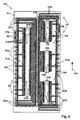
- the substrate 10 of the invention is represented in plan view in Fig. 1, and comprises a wafer 11 of silicon of a generically rectangular shape having length L and width H, with a left side 11 a, a right side 11b, an upper side 11 c and a lower side 11d.
- the length L, defined by the sides 11 a and 11 b, is greater than the width H, defined by the sides 11 c and 11d.
- the long sides 11a and 11b define a vertical or longitudinal direction, corresponding to the arrow 13, of the substrate 10, whereas the short sides 11 c and 11 d define a horizontal or transversal direction, corresponding to the arrow 14, of this substrate 10.
- this substrate 10 represents an essential component for the manufacture of an ink jet printhead, in particular of the type working on the principle of cyclically heating the ink contained in the head before emitting a plurality of ink droplets, and on this account also called thermal ink jet head.
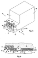
- a printhead of this type incorporating the substrate 10, is depicted in general in a perspective view in Fig. 5, where it is designated with the numeral 50, and in greater detail in a limited area in Fig. 6.
- the head 50 is provided with an outer shell 54 containing inside a volume of ink 61, and a nozzle plate 51, which in turn comprises a plurality of nozzles 52 suitable for ejecting ink droplets 58 on a printing medium 59, such as a sheet of paper, for printing symbols, characters and images on the latter-named.
- a printing medium 59 such as a sheet of paper
- the head 50 is typically of the colour type and is adapted for ejecting droplets of various colours, formed from colour inks, to produce colour prints on the printing medium 59 according to widely known printing arrangements.
- a layer 64 of a suitable material such as a photopolymer, is coupled by lamination on the surface of the substrate 10, and then etched by means of a known process, for instance photoetching, in order to reproduce the hydraulic circuit suitable for conveying the ink 61 to the actuators 16.
- the nozzle plate 51 is secured on the layer 64, and accordingly made integral with the substrate 10, so that the nozzles 52 are arranged exactly in correspondence with the actuators 16.
- the substrate 10 is secured on the outer shell 54 in correspondence with a front side 53 of the printhead 50, which, when in use, is arranged facing the printing medium 59 for ejecting on the latter-named the droplets 58 of ink, as illustrated in Fig. 6.
- the substrate 10 is arranged on the printhead 50 with the long sides 11a and 11b oriented perpendicular to the printing direction, indicated by the arrow 57, according to which the printhead 50 moves forward and back in front of the printing medium 59, during the printing step, for ejecting the ink droplets.
- the arrow 14 which defines the horizontal direction of the substrate 10 is parallel to the motion assumed by the printhead 50, during the printing motion, while the arrow 13, which defines the vertical direction of the substrate 10, is disposed transversally to the direction of the printing motion.
- the substrate 10 is made according to a widely known process and not therefore described in detail herein starting from a silicon wafer, generally circular in shape, subdivided into a plurality of elementary areas each corresponding to a substrate 10 to be manufactured.
- this silicon wafer is subjected to a series of work steps, in correspondence with the various elementary areas, such as the deposition of certain layers of materials on the surface of the wafer, the subsequent etching of these layers, and the formation of through slots in each of the elementary areas.
- the wafer is cut along the edges of the various elementary areas so as to form a plurality of substrates 10, such as the one depicted in Fig. 1.
- the substrate 10 Inside the rectangular perimeter of the wafer 11, the substrate 10 comprises three slots 12a, 12b, and 12c of elongated shape and formed in such a way as to fully traverse the thickness of the wafer 11.
- slots 12a-12c may be made using various techniques during manufacture of the substrate 10, for example by selectively etching the surface of the wafer 11 by means of a sand-blasting process.
- each of the three slots 12a-12c has the function of conveying a corresponding colour ink coming from an ink reserve, in turn accommodated inside the shell 54 of the printhead 50.
- the three slots 12a-12c are arranged for receiving respectively a magenta ink, a cyan ink and a yellow ink from respective and distinct main tanks provided in the printhead 50, and for conveying these colour inks to the zone of the nozzles 52, so that they are selectively ejected in the form of droplets and thus form upon the printing medium, by composition of the colour dots corresponding to the droplets emitted, colour symbols, characters and images.
- the slots 12a-12c are arranged for receiving the colour inks from the respective tanks through corresponding hydraulic circuits hermetically separated from one another, so as to avoid all forms of contamination between one ink and another.
- These hydraulic circuits comprise various elements such as micro-ducts, chambers, filters, of appropriate dimensions to ensure correct feeding of the inks from the respective tanks to the nozzles zone.
- the substrate 10 on account of there being numerous slots, is typically intended for being applied in a colour printing context, for use with various colour inks, it may also be used on a black and white type head, or a mixed type head capable of both black and colour printing, in which case one or more of the slots 12a-12c may be arranged for conveying black ink.
- the three slots 12a-12c extend in the longitudinal direction parallel to the long sides 11a and 11b of the wafer 11, and therefore according to the vertical direction defined by the arrow 13, each one comprising two long sides or edges, opposite and parallel as also is the arrow 13, and two short edges defining an upper and a lower end of the slot.
- the three slots 12a-12c which are of substantially the same length longitudinally, are formed on the surface of the wafer 11 in such a way as to define a Y-shape configuration, in which the two slots 12a and 12b are arranged in an upper semi-portion 10a of the substrate 10, perfectly in a line one beside the other along the respective long sides and parallel to the direction 13, whereas the third slot 12c is arranged in a lower semi-portion 10b of the substrate 10 and is displaced, parallel to the direction 13, with respect to the couple formed by the other two slots 12a and 12b by a distance at least equal to or greater than the length of the latter-named.
- the upper slots 12a and 12b are arranged perfectly aligned and one in the shadow of the other, whereas the slot 12c is arranged completely displaced with respect to the slots 12a and 12b, with the upper end or edge of slot 12c positioned, in the direction 13, at a given distance D from the lower ends of the slots 12a and 12b.
- the slot 12c is arranged according to the Y-shape configuration in an intermediate position between the slots 12a and 12b, i.e. at about half of the pitch P, measured in direction 14, between the two slots 12a and 12b.
- the substrate also comprises three actuating banks, generically designated 16a, 16b, and 16c, corresponding respectively to the three slots 12a, 12b and 12c, in which each actuating bank is composed of a plurality of actuators 16 arranged around the corresponding slot and made in turn of micro-resistors.
- Each actuating bank, in sequence 16a, 16b and 16c, is divided into two rows, which are arranged each along a respective long edge of the corresponding slot, i.e. 12a, 12b, and 12c.
- the various rows formed by these actuators 16 extend practically along the entire length of the long opposite edges of the corresponding slots 12a-12c, at a very short distance from these edges, and therefore assume an extension in the longitudinal direction which is practically the same for all the rows of actuators.
- the different rows of actuators which make up the actuating banks 16a, 16b and 16c and which are formed along the edges of the slots 12a-12c, are in turn subdivided into elementary groups, designated with the numeral 17 and, for instance, each made up of three or four aligned and adjacent actuators, in which these groups are arranged in succession, but which are slightly slanting one with respect to the other.
- This configuration of the actuators 16, also termed “staggered” configuration, has in particular the purpose of avoiding the actuators 16, adjacent to one another, being excited simultaneously, with the resultant danger of causing disturbance and interference of a hydraulic nature, the so-called hydraulic intermodulations, between two nearby nozzles, during operation of the printhead 50 incorporating the substrate 10.
- the actuators 16 arranged adjacently in each actuating bank 16a-16c are always slightly staggered in the direction 14, corresponding in turn to the direction of motion of the head 50, so that two actuators 16, arranged close to one another, transit at different times in front of an ideal line parallel to the direction 13, and must not therefore be excited simultaneously to print two dots lying in this direction 13.
- the arrangement of the nozzles 52 on the surface of the nozzle plate 51 exactly reproduces the arrangement of the actuators 16 on the long opposite sides of the slots 12a-12c of the substrate 10.
- the nozzles 52 of the plate 51 define a Y-shape configuration formed by three pairs of rows of nozzles, in which each pair of rows of nozzles corresponds to one slot of the substrate 10.
- the first pair is formed by the rows 52a and 52a' of nozzles, and corresponds to the slot 12a
- the second pair is formed by the rows 52b and 52b' and corresponds to the slot 12b
- the third pair is formed by rows 52c and 52c' and corresponds to the slot 12c.
- the actuators 16, made as stated of micro-resistors, are struck by the ink conveyed by the slots 12a-12c and are selectively heated impulsively, so as to bring the ink that is in their immediate vicinity rapidly to boiling point.
- each actuator 16 excited results in the formation, in its immediate vicinity, of a bubble of ink vapour which, in turn, by expanding, compresses the ink disposed in the zone about the excited actuator, thereby determining a wave of pressure that causes the ejection of an ink droplet through the nozzle corresponding to that excited actuator.
- the substrate 10 also comprises a plurality of drive circuits, also called drivers and designated with the numeral 18 in Fig. 1, which are arranged for controlling each actuator 16 in a selective way through suitable control signals.
- the tracks that connect the drive circuits 18 with the various actuators 16 are designated with the numeral 19, and constitute a very dense network, represented only in part and by way of example in Fig. 1, wherein the various connection tracks 19, without interfering with one another, perform the function of carrying the control signals to each actuator 16.
- these drive circuits 18 are not represented in detail but merely schematically in a dot and dash line, and are generically subdivided into three portions, respectively 18a, 18b and 18c, each arranged about a corresponding actuating bank, in the order 16a, 16b and 16c.
- each portion 18a, 18b and 18c of the drive circuits 18 extends on the surface of the substrate 10 adjacently to and at opposite ends with respect to the corresponding actuating bank 16a, 16b and 16c, but in an area slightly further away from the relative slots 12a, 12b and 12c.
- the various portions 18a, 18b and 18c of the drive circuits 18 assume a generically rectangular shape, and are arranged parallel to and around the rows of actuators 16 placed along the long edges of the slots 12a-12c.
- These drive circuits 18 possess known characteristics and are substantially made of a multiplicity of transistors or equivalent circuits, or other elementary circuits, in particular suitable for being addressed to work as switches and/or breakers.
- the drive circuits 18 are made on the surface of the substrate 10 with processes that are also widely known, for instance by depositing and selectively etching one or more layers of certain materials, and typically using technologies consolidated for making integrated circuits.
- these drive circuits 18 are reciprocally interconnected so as to define a matrix structure through which to address and therefore selectively drive the various actuators 16 with a low number of signals, and with a corresponding low number of terminals made on the substrate 10.
- the substrate 10 also comprises a plurality of terminals, generically designated with the numeral 21 and also called “pads”, which are electrically connected to the drive circuits 18 and are arranged along the vertical sides 11a and 11b of the substrate 10 for receiving from the outside the signals intended for selectively driving the actuators 16, as will be better described in the following.
- each terminal 21 is associated with a corresponding track for transmitting the signals received to the various circuits of the substrate 10.
- These terminals 21 are defined by the grid-like structure of the drive circuits 18 and are therefore considerably lesser in total number than the actuators 16.
- the terminals 21 are divided into a first and a second addressing group in which, as in a grid, the terminals belonging to the first addressing group and the terminals belonging to the second addressing group are suitable for defining in combination and unambiguously each actuator 16.
- terminals 21 of the first addressing group are designated with the numeral 21a and are represented alone without the corresponding track, while those of the second addressing group are designated with 21b and are represented with at least a portion of the corresponding track, in turn drawn with a dashed line at 45° and uniform step.
- the terminals 21a and 21b of the two groups are arranged in alternation along the vertical sides 11a and 11b of the substrate 10.
- terminals 21a and 21b of each addressing group are arranged for receiving as input, from the control circuit of the printer that the head 50 is mounted on, the signals that selectively command the actuators 16 by means of the drive circuits 18.
- the actuators 16 of the various actuating banks can be selectively addressed and driven through a combination of two signals sent to the terminals 21, so that, as already said, the number of terminals 21 actually needed to drive the actuators may be much less than that of the terminals 21 themselves.
- a given actuator 16 may be unambiguously addressed and commanded through a first and a second input signal, in which the first signal is sent to a given terminal 21 a belonging to the first addressing group, and the second signal is sent to another terminal 21 b belonging to the second addressing group.
- the signals received by terminals 21a are essentially logic type, i.e. characterized by currents of very feeble intensity, and generally have the function of enabling the ports of the transistors that comprise the drive circuits 18 in order to selectively address the actuators 16.
- the signals passing through the terminals 21b correspond to the power which is absorbed by the actuators 16 when they are activated and are thus characterized by current levels that are much higher than the signals fed to the terminals 21 a.
- the terminals 21 are divided into four groups or portions designated respectively with numerals 21-1, 21-2, 21-3 and 21-4, with the portions 21-1 and 21-2 arranged on the left side 11a, and the portions 21-3 and 21-4 arranged on the right side 11b.
- the terminals 21 a belonging to the first addressing group are connected to the drive circuits 18 through a plurality of tracks or lines, also called "buses", which are grouped and arranged one beside the other so as to define bunches 22 of tracks.
- bunches of tracks 22 are schematically represented in Fig. 1 with a dashed line formed by slanting lines in groups of two, and extend in a direction parallel to the edges of the substrate 10.
- the tracks comprising the bunches 22 are reduced in width with respect to the tracks, described in greater detail later, which transmit the through signals via the terminals 21 b.
- the bunch of tracks 22 is made in a first metallization process and subsequent selective etching on a lower layer of the substrate 10, upon which other layers will be deposited to produce other circuits, as will be better described in the following.
- bunches of tracks 22 comprises five main rectilinear portions, indicated 22a, 22b, 22c, 22d and 22e, which extend adjacent and parallel to corresponding portions of the drive circuits 18 in the vertical direction 13, in which in particular the portion 22a separates, on side 11 a, group 21-1 from group 21-2 of terminals 21b, whereas the portion 22b separates, on side 11b, group 21-3 from group 21-4 of terminals 21b.
- the bunches of tracks 22 also comprise portions 22f and 22g oriented parallel to the direction 14 for connecting the vertical portions of the bunches 22 to one another.
- the bunches of tracks 22 permit the signals received by the terminals 21 a to reach those components of the drive circuits 18 adapted for driving the actuators 16 selected in function of the printing program that controls emission of the droplets.
- the terminals 21 b of the second addressing group are connected with the drive circuits 18 through a plurality of other tracks, indicated 23, which, as already anticipated, are characterized by the fact that they are of greater width than the tracks, described above, defining the bunches 22.
- the tracks 23 generally have the function of transmitting the currents and therefore the power absorbed by the resistors that constitute the actuators 16, when they are heated impulsively to determine ejection of the droplets.
- These tracks 23 are partially represented in Fig. 1 with a dashed line of uniform step at 45 degrees and are made by the selective etching of a metallic layer, in turn deposited in a second metallization process above the layer corresponding to the bunches of tracks 22, after being suitably isolated from the latter.
- the tracks 23 run above the tracks of the bunches 22 in such a way that they straddle them without creating short-circuits with them.
- the tracks 23 each extend between a corresponding terminal 21 b and a zone adjacent to the row of actuators 16, where the tracks 23 widen, forming a T-shape end, so as to connect to the common terminals of a group of adjacent resistors which make up the actuators 16.
- the track 23a extends on top of the bus 22 between the relative terminal 21 b and the zone of the actuators 16, where the track 23a assumes, as said, a greater width than the remaining portion adjacent to the terminal 21 b, so as to connect to the common point of a large number of actuators 16.
- the terminals 21 b are variously positioned along the sides 11a and 11b of the substrate 10..
- four terminals 21b constitute the portion 21-1, of which two are connected with two respective groups of actuators 16 arranged on the left side of the slot. 12a, and the other two are connected with two respective groups of actuators 16 arranged on the right side of the slot 12a.
- terminals 21b constitute the portion 21-3, of which two are connected with two respective groups of actuators 16 arranged on the left side of the slot 12b, and the other two are connected with two respective groups of actuators 16 arranged on the right side of the slot 12b.
- terminals 21 b are placed on the sides 11 a and 11b under the portions 22a and 22b of the bunches 22 and are connected with the remaining groups of actuators 16, adjacent to the slots 12a and 12b, which are not connected with the terminals 21 b mentioned above and constituting the portions 21-1 and 21-3.
- the terminals 21b corresponding to the actuators 16 adjacent to the two slots 12a and 12b, arranged in the upper portion 10a of the substrate 10, are disposed symmetrically on top of and under each slot 12a and 12b, so as to allow the tracks 23 which feed the actuators 16 of the slots 12a and 12b to extend according to regular, limited paths.
- the terminals 21 are electrically connected via a flexible cable 56 with a plurality of contacts or pads 62 arranged on an outer side, not shown, of the head 50, which is oriented according to a plane perpendicular to the front side 53.
- the flexible cable 56 also called “flat cable”
- the flexible cable 56 defines a plurality of tracks 63 which connect each terminal 21 with a corresponding pad 62.
- the flexible cable 56 is glued on the surface of the shell 54, both on the front side 53 and on the side not in view bearing the contacts 62, and is bent in correspondence with an edge 60 arranged between these two sides.
- the pads 62 are provided for connecting with corresponding contacts arranged in the suitable seat of the printer in which the printhead 50 itself is removably accommodated.
- the terminals 21 can receive the signals sent by the printer control circuit, before addressing them through the tracks 22 and 23 to the drive circuits 18 and, as a result, selectively activating the actuators 16.
- the substrate 10 also comprises an earth network 31 which is represented with a criss-cross dashed line and is made up of a multiplicity of portions, indicated by way of example with 31a, 31b, 31c, which are interconnected with one another, and which run along the surface of the substrate 10 between the various slots 12a-12c.
- an earth network 31 which is represented with a criss-cross dashed line and is made up of a multiplicity of portions, indicated by way of example with 31a, 31b, 31c, which are interconnected with one another, and which run along the surface of the substrate 10 between the various slots 12a-12c.
- This earth network 31 has essentially the function of conveying feedback currents generated during activation of the actuators 16 to the outside of the substrate 10 and is connected with corresponding earth terminals, indicated with 31d, arranged along the edges of the same substrate 10.
- two earth terminals 31d may be arranged respectively in an upper zone of the side 11a and in an upper zone of the side 11b, between the group of adjacent terminals 21b constituting the portions 21-1 and 21-3 and the portions 22a and 22b of the bunches 22 arranged on the sides 11a and 11b.
- Other earth terminals 31d may be variously arranged along the lower zones of the sides 11a and 11b, not occupied by the bunch 22, between terminals of type 21a and 21b.
- the substrate 10 comprises a plurality of protecting elements, indicated with 32 and represented with dark-filled areas, which are suitably arranged in numerous zones of the substrate 10 for the purpose of protecting the various circuits, and most particularly for avoiding the accidental overvoltages and electrostatic discharges which could damage these circuits.
- the protecting elements 32 are arranged along the edges 11a and 11b between each terminal 21 and the one adjacent thereto, and are connected at one end with the track they have to protect and at the other end with the earth network 31.
- this substrate lies in the disposition and orientation of the lines of terminals 21 with respect to the slots 12a-12c arranged for conveying the ink, and in the corresponding actuating banks 16a-16c.
- the substrate 10 may to advantage be produced with a low value of width H.
- the terminals 21b which receive the power signals for the actuating banks 16a and 16b adjacent to the upper slots 12a and 12b are arranged symmetrically, partly in an upper zone and partly in a lower zone, with respect to the slots 12a and 12b and as close as possible to them, and therefore to the corresponding actuating banks 16a and 16b.
- the tracks 23, having a T-shape end, that connect the terminals 21b with the groups of actuators 16 adjacent to the slots 12a and 12b assume as reduced an extension as possible and one that is therefore optimal in terms of the dissipation of energy and quality of the signals transmitted.
- terminals 21 a adapted for receiving the logic signals for addressing of the actuators 16 of the actuating banks 16a-16c adjacent to the three slots 12a-12c are arranged, in alternation with terminals 21b associated with the actuating bank 16c, at opposite ends with respect to the fatter-named slot 16c and along lower portions of the opposite ends 11a and 11b having an extension substantially corresponding to that of the slot 12c.
- the length L of the substrate 10 may to advantage assume a low value with respect to the substrates of the known art
- each actuating bank the 68 actuators of each row are arranged in a line in a vertical direction according to a step 'equal to 1/300 of an inch, also indicated 1/300", i.e. equal to 0.0846 mm, whereas the two rows are staggered still in the vertical direction by a distance equal to one half of the step between the actuators of each row.
- the actuators of the two rows considered as a whole are reciprocally staggered according to a step of 1/600" in the vertical direction.
- the actuators 16 of each actuating bank 16a-16c and the corresponding ejection nozzles 52 are capable of printing with a printing resolution of 1/600°, when the printhead 50 moves during its printing stroke in a direction parallel to the arrow 57, with the actuating banks 16a-16c oriented perpendicular to this printing motion.
- the distance D that separates, in the vertical direction 13, the two upper slots 12a and 12b from the lower slot 12c, and therefore the two actuating banks 16a and 16b from the actuating bank 16c, may be between 0.45 and 0.95 mm.
- the length L of the substrate 10 assumes a value of about 15 mm.
- the number of terminal 21 that may be arranged along the two sides 11a and 11b of the substrate 10 can be variable, depending on the characteristics of the drive circuits 18, on their grid structure, and on the number of actuators 16 to be commanded.
- the terminals 21 may be divided, on each side 11a or 11b, into an upper group and a lower group separated by a portion of the bunch 22 of lines, in which the upper group is made up of a certain number, for example four, of terminals of type 21b and is arranged adjacent to an end of the respective side 11a or 11b, and the lower group is made up of a greater number of terminals 21, both of the type 21a and of the type 21b.
- the remaining length of the edges 11a and 11b is more than sufficient to support a suitable number of terminals for control of the actuators 16.
- the substrate 10 assumes a considerably more reduced area than that of the known substrates bearing a roughly equivalent number of actuators.
- the substrate 10 with the three slots 12a, 12b and 12c, and with the actuators 16 divided into three groups arranged along the opposite sides of the respective slots may be used for manufacturing a colour ink jet printhead capable of operating with a print definition of 1/600 of an inch, in which in particular the actuators 16 of the first group of actuators arranged along the sides of the slot 12a are provided for commanding the ejection of droplets of a first colour, the actuators of the second group arranged along the sides of the slot 12b are provided for commanding the ejection of droplets of a second colour, and the actuators of the third group arranged along the sides of the slot 12c are provided for commanding the ejection of droplets of a third colour.
- FIG. 2 A second embodiment of the substrate according to the invention is depicted in Fig. 2 and is generically indicated with the numeral 110.
- the substrate 110 comprises a rectangular silicon plate 111 having two long opposite sides 111a e 111b which are oriented in a vertical direction 113, and two short sides 111c and 111d parallel to a horizontal direction 114, corresponding in turn to the motion of the substrate 110 during printing.
- the substrate 110 differs from the substrate 10 in that, instead of three, it has four slots 112a, 112b, 112c and 112d, parallel to one another, extending in the lengthwise direction parallel to the vertical direction 113.
- slots 112a, 112b, 112c and 112d are divided into an upper pair consisting of the slots 112a and 112b and are arranged in an upper semi-portion 110a of the substrate 110, and into a lower pair consisting of the slots 112c and 112d and arranged in a lower semi-portion 110b of the substrate 110.
- the slots 112a-112b and the slots 112c-112d of each pair are arranged side by side and each perfectly in the shadow of the other if observed in the horizontal direction 114.
- the slots 112a and 112c are arranged in perfect alignment if observed according to the vertical direction 113.
- the slots 112a-112d define a configuration, alternative to the Y-shape configuration relative to the substrate 10, that is rectangular, in Which the upper slots 112a and 112b are staggered with respect to the lower slots 112c and 112d in the direction 113 by a distance D1, and both the upper slots 112a-112b and the lower slots 112c-112d are arranged side by side lengthwise at a same distance or step P1.
- Three of the slots 112a-112d may be arranged for conveying colour inks, while the remaining slot may be arranged for conveying black ink.
- the substrate 110 also comprises a plurality of parts, such as actuators, drive circuits, etc... which are perfectly similar to those already described with reference to the substrate 10, and in particular four actuating banks 116a, 116b, 116c and 116d, each consisting of a plurality of actuators 116 arranged along both the long opposite edges of a corresponding slot, in order 112a, 112b, 112c and 112d, a plurality of drive circuits 118, and a plurality of connecting tracks 119 for connecting the drive circuits 118 with the actuators 116.
- actuating banks 116a, 116b, 116c and 116d each consisting of a plurality of actuators 116 arranged along both the long opposite edges of a corresponding slot, in order 112a, 112b, 112c and 112d, a plurality of drive circuits 118, and a plurality of connecting tracks 119 for connecting the drive circuits 118 with the actuators 116.
- the substrate 110 also comprises a plurality of terminals 121, arranged along the sides 111a and 111b, and a plurality of tracks 122 for connecting each terminal 121 with the drive circuits 118.
- the tracks 122 are normally grouped in the form of bunches and extend along the surface of the substrate 190 between terminals 121 and the drive circuits 118 according to an optimal configuration, in particular such as to occupy the lowest possible portion of surface of the substrate 110.
- the terminals 121 are divided into two groups of terminals 121a and 121b, reciprocally intertwined, in order to define a grid suitable for selectively addressing, by the combination of a signal received by a given terminal 121 a of the first group and of another signal received by a given terminal 121b of the second group, a given actuator 116.
- the tracks and bunches of tracks that connect the terminals 121 with the drive circuits 118 are represented schematically with various types of dash, overlaid one on top of the other.
- the method of using the substrate 110 during the manufacturing process of a corresponding ink jet printhead is perfectly similar to the substrate 10.
- the substrate 110 has the advantage, with respect to known substrates, of having the terminals 121 arranged, as stated, for receiving the external control signals intended for selectively commanding the ejection actuators 116; which are arranged in a line parallel to the direction of orientation of the slots 112a-112d and along two opposite sides on the outside of the zone of the same slots 112a-112d.
- connection cable which, in the structure of the printhead incorporating the substrate 110, is intended for conveying control signals to the terminals 121 from the zone of the contacts for the electrical connection with the outside of the printhead.
- FIG. 3 A third embodiment of the substrate the subject of this invention is illustrated in Fig. 3 and is designated with the numeral 210.
- the substrate 210 comprises a rectangular silicon plate 211 having two long opposite sides 211a and 211b which are oriented in a vertical direction 213, and two short sides 211 c and 211 d oriented in a horizontal direction 214, corresponding in turn to the motion of the substrate 210 during printing.
- the substrate 210 also comprises four slots 212a, 212b, 212c and 212d, which extend parallel to one another lengthwise according to the vertical direction 213.
- slots 212a, 212b, 212c and 212d are divided into an upper pair consisting of the slots 212a and 212b and arranged in an upper semi-portion 210a of the substrate 210, and into a lower pair consisting of the slots 212c and 212d and arranged in a lower semi-portion 210b of the substrate 210.
- the slots 212a-212b and the slots 212c-212d of each pair are disposed side by side and each perfectly in the shadow of the other, if observed in the horizontal direction 114 but, unlike the substrate 110, the slots 212a-212b of the upper pair and the slots 212c-212d of the lower pair are disposed, if observed according to the vertical direction 113, staggered by a distance equal to about half of the step P2 between the slots of each pair.
- the slots 212a-212d define a staggered rectangular type configuration, alternative to both the Y-shape configuration of the substrate 10 and the perfectly symmetrical and rectangular configuration of the substrate 110.
- the upper slots 212a and 212b are staggered with respect to the lower slots 212c and 212d in the direction 213 by a distance D2, and furthermore, as already said, the upper slots 212a-212b and the lower slots 212c-212d are arranged reciprocally staggered in the direction 214 by a distance equal to about half of their step P2.
- the substrate 210 also comprises other parts such as actuating banks consisting of a plurality of ejection actuators, drive circuits, terminals, connecting tracks, etc... which are perfectly similar to those already described with reference to the preceding embodiments.
- the substrate 210 comprises a plurality of actuators 216 arranged along the edges of the four slots 212a-212d and a corresponding plurality of terminals 221 arranged in a line along the two sides 211a and 211b, accordingly parallel to the direction of extension of the slots 212a-212d, in which these terminals 221 are adapted for receiving the external signals for selectively addressing and driving the actuators 216.
- the terminals 221 of the substrate 210 are divided into two addressing groups, in accordance with a grid-type addressing structure of the actuators 216, in which the terminals of the first addressing group are indicated 221a and are adapted for receiving logic signals, characterized by having currents of feeble intensity, whereas the terminals belonging to the second addressing group are indicated 221b and are adapted for receiving power signals, characterized by currents of higher intensity.
- the terminals 221a of the first addressing group are connected with the circuits that drive the actuators 216 through a plurality of tracks that run side by side along the surface of the substrate 210 in such a way as to define bunches of tracks designated with the numeral 222.
- bunches extend in various zones of the substrate 210 between the slots 212a-212d and between the respective actuating banks.
- Fig. 1 illustrates a configuration of the substrate 210 in which the terminals 221 are arranged along the entire length of the sides 211a and 211b, and immediately adjacent to the latter-named, with the bunches 222 which are arranged slightly further back along the sides 211a and 211b, with respect to the terminals 221.
- the substrate 210 in which for example the terminals 221 may be missing along given stretches of the sides 211a and 211b, with- in place of these - portions of the bunches 222.
- the bunch of tracks 222 may extend immediately adjacent to the side 211a, or to the side 211b, or to both the sides, along stretches having a length substantially corresponding to that of the slots 212a-212d, so as to have the terminals 221 located in the remaining zones of the sides 211a and 211b not occupied by the bunch 222.
- a fourth embodiment, generically designated with the numeral 310, of the substrate the subject of this invention is represented schematically in Fig. 4.
- this fourth embodiment of the substrate corresponding to those of the first embodiment 10 shall be designated with the same reference numerals plus 300.
- the substrate 310 comprises a thin rectangular plate of silicon 311 defining one right side or edge 311a and a left side or edge 311b, and which also has one long slot 312a arranged along a left portion of the substrate 310, and three short slots, indicated respectively with 312b, 312c and 312d, arranged along a left portion of the substrate 314, wherein all four slots are made through the thickness of the plate 311 and are oriented in a vertical direction 313 parallel to the sides 311a and 311b.
- the three short slots 312b, 312c and 312d are arranged in a line among one another, alongside the right side of the long slot 312a.
- a plurality of actuators 316 are arranged along the opposite sides, parallel to the direction 313, of each slot of the substrate 310, in such a way as to form four actuating banks 316a, 316b, 316c, and 316d corresponding respectively to the slots 312a, 312b, 312c and 312d.
- drive circuits indicated generically with 318 and arranged adjacent to and around the actuating banks 316a, 316b, 316c and 316d in various zones of the surface of the substrate 310, are associated with the actuators 316 for selectively controlling each one thereof.
- the substrate 310 further comprises a plurality of terminals 321 which are suitable for receiving the external signals for controlling the drive circuits, and by means of the latter-named for selectively driving the actuators 316.
- These terminals 321 are arranged in a line along the sides 311a and 311b, i.e.
- the terminals 321 are disposed along the entire length of the edges 311a and 311b, without any portions of tracks or bunches of tracks interposed for connection of the terminals 321 with the drive circuits 318.
- the substrate 310 further comprises a multiplicity of protecting elements 332, shown only in part in Fig. 4, whose function is to protect the circuits 318.
- the long slot 312a is arranged for conveying a black ink, whereas the three slots 312b, 312c and 312d are arranged each for conveying a corresponding colour ink, to the corresponding ejection actuators.
- the three colours conveyed by the three slots 312b, 312c and 312d correspond to the three basic colours so as to enable the formation, by composition of dots printed with these colours, of colour print-outs.
- a substrate of this type may serve to produce a colour ink jet printhead
- the first actuating bank 316a consists in toto of 208 nozzles arranged in two rows side by side along the long opposite sides of the slot 312a, and is adapted for ejecting black ink droplets
- the other three actuating banks 312b, 312c, and 312d are each made up of 64 nozzles arranged in two rows side by side along the long opposite sides of the corresponding slot, namely 312b, 312c and 312d, for ejecting respectively the three basic colour inks.
Landscapes
- Particle Formation And Scattering Control In Inkjet Printers (AREA)
- Inks, Pencil-Leads, Or Crayons (AREA)
- Ink Jet (AREA)
Abstract
Description
Claims (19)
- Substrate (10; 110; 210; 310) for an ink jet printhead (50), in particular though not exclusively of the colour type, comprising:wherein at least two (12a, 12b; 112a, 112b; 212a, 212b; 312a, 312b) of said at least three slots are arranged on the surface of said substrate (10; 110; 210; 310) one beside the other along the respective long sides, and therefore parallel to said given vertical direction (13; 113; 213; 313), andat least three actuating banks (16a, 16b, 16c; 116a, 116b, 116c, 116d; 316a, 316b, 316c, 316d) and at least three slots (12a, 12b, 12c; 112a, 112b, 112c, 112d; 212a, 212b, 212c, 212d; 312a, 312b, 312c, 312d) of elongated shape corresponding to said three actuating banks (16a, 16b, 16c; 116a, 116b, 116c, 116d; 316a, 316b, 316c, 316d), said at least three slots (12a, 12b, 12c, 112a, 112b, 112c, 112d; 212a, 212b, 212c, 212d; 312a, 312b, 312c, 312d) being oriented lengthwise parallel to a given vertical direction (13; 113; 213; 313), each of said at least three slots (12a, 12b, 12c; 112a, 112b, 112c, 112d; 212a, 212b, 212c, 212d; 312a, 312b, 312c, 312d) being made through the thickness of said substrate (10, 110; 210; 310) for conveying a flow of ink to the corresponding actuating bank (16a, 16b, 16c; 116a, 116b, 116c, 116d; 316a, 316b, 316c, 316d), each of said three actuating banks (16a, 16b, 16c; 116a, 116b, 116c, 116d; 316a, 316b, 316c, 316d) consisting in turn of a plurality of ejection actuators (16; 116; 216; 316) arranged substantially in a line along the long opposite sides of the corresponding slot,a plurality of terminals (21, 21a, 21b; 121, 121a, 121b; 221; 321, 321 a, 321b) arranged on the surface of said substrate (10; 110; 210; 310) for receiving a plurality of external signals suitable for selectively addressing and driving said actuators (16; 116; 216; 316), anda plurality of drive circuits (18; 118; .318) arranged between said terminals (21, 21a, 21b; 121, 121a, 121b; 221; 321, 321a, 321b) and said actuating banks (16a, 16b, 16c; 116a, 116b, 116c, 116d; 316a, 316b, 316c, 316d) for selectively controlling, in response to the external signals received by said terminals (21; 121; 221; 321), the ejection actuators (16; 116; 216; 316) of said three actuating banks (16a, 16b, 16c; 116a, 116b, 116c, 116d; 316a, 316b, 316c, 316d), said drive circuits (18; 118; 318) extending, around said actuating banks (16a, 16b, 16c; ,116a, 116b, 116c, 116d), along portions of the surface of said substrate, of elongated shape and substantially parallel to said at least three slots (12a, 12b, 12c; 112a, 112b, 112c, 112d; 212a, 212b, 212c, 212d; 312a, 342b, 312c, 312d) and therefore to said given vertical direction (13; 113; 213; 313), said drive circuits (18; 118; 318) being interconnected according to a grid configuration defining said terminals (21, 21a, 21b; 121, 121a, 121b; 221; 321) and such as to allow said ejection actuators (16; 116; 216; 316) to be addressed with a lesser number of terminal (21; 121; 221; 321) than that of said ejection actuators (16; 116; 216; 316),
wherein said terminals (21, 21a, 21b; 121, 121a, 121 b; 221; 321, 321 a, 321 b) associated with the drive circuits (18; 118; 318) for selectively addressing and driving the ejection actuators (16; 116; 216; 316) are arranged in a zone external to said at least three slots (12a, 12b, 12c; 112a, 112b, 112c, 112d; 212a, 212b, 212c, 212d; 312a, 312b, 312c, 312d) and to said drive circuits (18; 118; 318), substantially in a line with one another parallel to said given vertical direction (13; 113; 213; 313). - Substrate (10; 110; 210) according to claim 1, characterized in that a first (12a; 112a; 212a) and a second (12b; 112b; 212b) of said at least three slots are of substantially equal length and are arranged on an upper portion (10a; 110a; 210a) of said substrate (10; 110; 210), one beside the other according to a given step (P; P1; P2) substantially over the entire extent of the respective long sides, parallel to said given vertical direction (13; 113; 213), so that the two actuating banks (16a, 16b; 116a, 116b) corresponding respectively to said first (12a; 112a; 212a) and to said second slot (12b; 112b; 212b) are arranged side by side on said upper portion (10a; 110a; 210a),
and in that a third (12c; 112c, 112d; 212c, 212d) of said at least three slots is arranged, on a lower portion (10b; 110b; 210b) of said substrate (10; 110; 210), completely displaced with respect to the other two slots (12a, 12b; 112a, 112b; 212a, 212b) along said given vertical direction (13; 113; 213), according to a given distance (D; D1; D2), so that the actuating bank (16c; 116c, 116d) corresponding to said third slot (12c; 112c, 112d; 212c, 212d) is arranged on said lower portion (10b; 110b; 210b) and is displaced with respect to the other two (16a, 16b; 116a, 116b) along said vertical direction (13; 113; 213). - Substrate (10) according to claim 2, characterized in that the third (12c) of said at least three slots (12a, 12b, 12c), arranged in the lower portion of said substrate (10), is displaced with respect to the other two slots (12a, 12b), in turn arranged in the upper portion of said substrate (10), along a given horizontal direction (14) perpendicular to said given vertical direction (13), according to a distance equal to about half of the step (P) between the other two slots (12a, 12b), so that said three slots (12a, 12b, 12c) together define a Y-shape configuration on the surface of said substrate (10).
- Substrate (110) according to claim 2, characterized in that it comprises, in addition to said first (112a) and to said second (112b) slots arranged in the upper portion (110a) of said substrate (110), a third (112c) and a fourth (112d) slot substantially equal in length and arranged in the lower portion (110b) of said substrate (110), wherein said first (112a), second (112b), third (112c) and fourth (112d) slots are substantially aligned with one another two by due, both if observed along said given horizontal direction (113) and if observed along said given vertical direction (114), so that the four slots (112a, 112b, 112c; 112d) together define a rectangular type configuration on the surface of said substrate (110).
- Substrate (210) according to claim 2, characterized in that it comprises, in addition to said first (212a) and to said second (212b) slots arranged in the upper portion (210a) of said substrate (210), a third (212c) and a fourth (212d) slot substantially equal in length and arranged in the lower portion (210b) of said substrate (210), wherein said third (212c) and fourth (212d) slots are, like said first and second slots, arranged beside one another substantially over the entire extent of the respective long sides, according to a step substantially equal to that between said first and second slot (212a, 212b), but are however displaced, with respect to the latter (212a, 212b), along said given horizontal direction (214) perpendicular to said given vertical direction (213), by a distance equal to about half of said step (P2), so that said four slots (212a, 212b, 212c, 212d) together define a staggered rectangular type configuration on the surface of said substrate (210).
- Substrate (310) according to claim 1, characterized in that it comprises a first long slot (312a), and three short slots (312b, 312c, 312d) parallel to one another according to said given vertical direction (313), wherein said three short slots (312b, 312c, 312d) are arranged substantially in a line with one another lengthwise, i.e. parallel to said given vertical direction, alongside said first long slot (312a).
- Substrate (10, 110) according to claim 1 or 2, wherein said terminals (21; 121) are connected with said drive circuits (18; 118) through a plurality of adjacent tracks forming a bunch (22; 122) for the transmission to the drive circuits of the signals received by the terminals (21; 121), characterized in that said bunch (22; 122) extends on the surface of said substrate (10; 110) between said at least three slots (12a, 12b, 12c; 112a, 112b, 112c, 112d), and in particular comprises at least a rectilinear portion (22c) which extends between the two slots (12a, 12b; 112a, 112b) which are arranged one beside the other on said upper portion (10a; 110a) of the substrate (10; 110), and also parallel thereto.
- Substrate (10) according to claim 7, characterized in that said terminals (21, 21a, 21 b) are grouped in four portions (21-1,21-2, 21-3, 21-4), two of which (21-1, 21-2) are arranged along a first side (11a) of said substrate and are separated by a portion of the bunches of tracks (22) which connect said terminals with the drive circuits (18), and the remaining two (21-3, 21-4) are arranged along the second side (11b) opposite the first of said substrate (10), these also being separated by a portion of the bunches (22) of tracks.
- Substrate according to claim 1, characterized in that said terminals (21; 121; 221; 321) are arranged one beside the other along two opposite sides (11a, 11b; 111a, 111b; 211a, 211b; 311a, 311b) of said substrate (10; 110; 210; 310), parallel to said given vertical direction (13; 113; 213; 313).
- Substrate (310) according to claim 9, characterized in that said terminals (321, 321a, 321b) are arranged parallel to said given vertical direction (313), substantially along the entire length of said sides (311 a, 311 b).
- Substrate according to claim 9, characterized in that said terminals (21; 121; 221; 321) are divided into a first addressing group and into a second addressing group defined by the grid structure of said drive circuits (18; 118; 218; 318), wherein the terminals (21a; 121a; 321a) belonging to said first addressing group are electrically connected to said drive circuits (18; 118; 218; 318) via one or more bunches (22; 122) of adjacent tracks, and the terminals (21b; 121b; 321 b) belonging to said second addressing group are each electrically connected to a plurality of terminals common to a group of actuators (16; 116; 216; 316).
- Substrate according to claim 11, characterized in that the tracks (23) which connect the terminals (21b; 121b; 321b) belonging to the second addressing group to the various groups of actuators (16; 116; 216; 316) are of substantially greater thickness than the tracks that define the bunches (22; 122) which connect the terminals (21 a; 121a; 321a) belonging to the first addressing group to said drive circuits (18; 118; 218; 318).
- Substrate according to claim 11, characterized in that said terminals (21a, 21b; 121a, 121b; 321a, 321b) belonging to said first and to said second addressing group are arranged in reciprocal alternation along said two opposite sides (11a, 11b) of said substrate (10).
- Substrate according to claim 11, characterized in that it comprises a first and a second plurality (21-1, 21-3) of terminals (21b) arranged side by side with one another and belonging to said second addressing group, wherein said first (21-1) and said second (21-3) plurality of terminals are arranged in two zones adjacent respectively to an upper end of a first (11a) and to an upper end of a second (11b) of said opposite sides (11a, 11b) of said substrate (10), and wherein the terminals of said first plurality (21-1) are connected with the actuators (16) arranged along a first slot (12a), and the terminals of said second plurality (21-3) are connected with the actuators arranged along a second slot (12b).
- Substrate according to claim 14, characterized in that part of the terminals (21b) of each of said first and second plurality are connected with the actuators (16) arranged along one side of the corresponding slot (12a, 12b), and the remaining terminals (21b) of each of said first and second plurality are connected with the actuators (16) arranged along the opposite side of the corresponding slot (12a, 12b).
- Substrate according to any one of the previous claims, characterized in that it comprises an earth network (31) extending along the surface of said substrate (10) and having essentially the function of conveying to the outside of said substrate (10) the feedback currents that are generated during activation of the actuators (16), wherein said earth network (31) is connected with one or more corresponding earth terminals (31d) arranged along the sides of said substrate parallel to said given vertical direction (13).
- Ink jet printhead (50) characterized in that it comprises a substrate (10; 110; 210; 310) according to claim 1.
- Ink jet printhead (50) comprising:wherein at least two (12a, 12b) of said at least three slots and correspondingly at least two (16a, 16b) of said banks of ejection actuators (16) are arranged side by side with one another parallel to said vertical direction (13), anda nozzle plate (52) for the emission of droplets (58) of ink, said nozzle plate (52)
being provided with at least three banks of nozzles (52a, 52a', 52b, 52b', 52c, 52c'), distinct from one another, having an elongated shape and arranged parallel to a vertical direction (13), anda substrate (10) associated with said nozzle plate (52), having:at least three slots (12a, 12b, 12c) substantially rectilinear and parallel to said vertical direction (13), each of said at least three slots (12a, 12b, 12c) being formed through the thickness of said substrate for conveying a flow of ink to a corresponding bank of nozzles (52a, 52a', 52b, 52b', 52c, 52c'),at least three actuating banks (16a, 16b, 16c) corresponding to said at least three banks of nozzles (52a, 52a', 52b, 52b', 52c, 52c'), each of said three actuating banks being made up of a plurality of ejection actuators (16) arranged on said substrate along the opposite rectilinear sides of a corresponding slot (12a, 12b, 12c),a plurality of drive circuits (18) connected with the ejection actuators (16) of said three actuating banks (16a, 16b, 16c), said drive circuits (18) extending on said substrate (10) adjacency to said ejection actuators (16) so as to assume a configuration substantially parallel to said three actuating banks (16a, 16b, 16c) and therefore to said vertical direction (13), anda plurality of terminals (21, 21a, 21b) connected with said drive circuits (18) and suitable for receiving as input a plurality of external signals for selectively addressing and activating said ejection actuators (16), said terminals (21, 21a, 21b) being divided into two addressing groups defined by a grid structure of said drive circuits (18) to be able to selectively address and drive said ejection actuators (16) with a lesser number of terminals (21, 21a, 21b) than that of said ejection actuators (16),
wherein said terminals (21, 21a, 21b) connected with the drive circuits (18) and adapted for receiving the control signals of said at least three actuating banks (16a, 16b, 16c) are arranged externally to and perimetrally with respect to said drive circuits (18) along two opposite sides (11a, 11b) of said substrate, substantially parallel to said vertical direction (13). - Printhead (50) according to claim 17, wherein said substrate is arranged on a front side (53) of said head, comprising:wherein said contacts (62) are arranged on a contact side of said printhead oriented according to a plane substantially perpendicular to said front side (53), said contact side being adjacent to said front side (53) along an edge (60), and wherein said connecting cable (56) extends along both said front side and said contact side and is bent in correspondence with said edge.a plurality of contacts (62) corresponding to said terminals (21, 21a, 21b) for enabling the electrical connection of said printhead (50) with the outside, anda connecting cable (56) for connecting each of said terminals (21, 21a, 21b) with a corresponding contact (62),
Applications Claiming Priority (3)
| Application Number | Priority Date | Filing Date | Title |
|---|---|---|---|
| ITTO20010266 | 2001-03-21 | ||
| IT2001TO000266A ITTO20010266A1 (en) | 2001-03-21 | 2001-03-21 | SUBSTRATE FOR A HEAT INK JET HEAD, IN PARTICULAR OF THE COLOR TYPE, AND AN INCORPORATING PRINT HEAD SUCH ON |
| PCT/IT2002/000163 WO2002074545A1 (en) | 2001-03-21 | 2002-03-18 | Substrate for a thermal ink jet printhead, a colour printhead in particular, and ink jet printhead incorporation this substrate |
Publications (2)
| Publication Number | Publication Date |
|---|---|
| EP1372966A1 EP1372966A1 (en) | 2004-01-02 |
| EP1372966B1 true EP1372966B1 (en) | 2005-03-09 |
Family
ID=11458714
Family Applications (1)
| Application Number | Title | Priority Date | Filing Date |
|---|---|---|---|
| EP02722655A Expired - Lifetime EP1372966B1 (en) | 2001-03-21 | 2002-03-18 | Substrate for a thermal ink jet printhead, a colour printhead in particular, and ink jet printhead incorporating this substrate |
Country Status (7)
| Country | Link |
|---|---|
| US (1) | US7008047B2 (en) |
| EP (1) | EP1372966B1 (en) |
| AT (1) | ATE290467T1 (en) |
| DE (1) | DE60203167T2 (en) |
| ES (1) | ES2239714T3 (en) |
| IT (1) | ITTO20010266A1 (en) |
| WO (1) | WO2002074545A1 (en) |
Families Citing this family (12)
| Publication number | Priority date | Publication date | Assignee | Title |
|---|---|---|---|---|
| JP4350408B2 (en) | 2003-04-10 | 2009-10-21 | キヤノン株式会社 | Printhead substrate, printhead, and printing apparatus |
| EP1617999B1 (en) * | 2003-04-28 | 2011-01-05 | Panasonic Corporation | Ink jet head unit and ink jet recording apparatus mounted with the same |
| US7240997B2 (en) * | 2004-02-25 | 2007-07-10 | Hewlett-Packard Development Company, L.P. | Fluid ejection device metal layer layouts |
| CN1311974C (en) * | 2004-03-24 | 2007-04-25 | 财团法人工业技术研究院 | Printing device, inkjet head, inkjet head driving control circuit and control method thereof |
| CN100503248C (en) * | 2004-06-02 | 2009-06-24 | 佳能株式会社 | Head substrate, recording head, head cartridge, recorder, and method for inputting/outputting information |
| GB0503996D0 (en) * | 2005-02-26 | 2005-04-06 | Xaar Technology Ltd | Droplet deposition apparatus |
| US20060232627A1 (en) * | 2005-03-31 | 2006-10-19 | Lexmark International, Inc. | Power distribution routing to reduce chip area |
| US7290864B2 (en) * | 2005-09-30 | 2007-11-06 | Lexmark International, Inc. | Heater chips with a reduced number of bondpads |
| US7361966B2 (en) * | 2006-02-13 | 2008-04-22 | Lexmark International, Inc. | Actuator chip for inkjet printhead with electrostatic discharge protection |
| JP2015054410A (en) * | 2013-09-10 | 2015-03-23 | キヤノン株式会社 | Liquid discharge head and liquid discharge apparatus |
| CN106663656B (en) * | 2014-08-18 | 2018-09-11 | 惠普发展公司有限责任合伙企业 | Alternative ground wire for slot bay grounding |
| JP6708945B2 (en) * | 2015-10-30 | 2020-06-10 | セイコーエプソン株式会社 | Liquid ejector |
Family Cites Families (7)
| Publication number | Priority date | Publication date | Assignee | Title |
|---|---|---|---|---|
| US4812859A (en) * | 1987-09-17 | 1989-03-14 | Hewlett-Packard Company | Multi-chamber ink jet recording head for color use |
| US5030971B1 (en) | 1989-11-29 | 2000-11-28 | Xerox Corp | Precisely aligned mono- or multi-color roofshooter type printhead |
| US5455610A (en) | 1993-05-19 | 1995-10-03 | Xerox Corporation | Color architecture for an ink jet printer with overlapping arrays of ejectors |
| US5719605A (en) * | 1996-11-20 | 1998-02-17 | Lexmark International, Inc. | Large array heater chips for thermal ink jet printheads |
| US6123410A (en) | 1997-10-28 | 2000-09-26 | Hewlett-Packard Company | Scalable wide-array inkjet printhead and method for fabricating same |
| US6213587B1 (en) * | 1999-07-19 | 2001-04-10 | Lexmark International, Inc. | Ink jet printhead having improved reliability |
| US6318846B1 (en) * | 1999-08-30 | 2001-11-20 | Hewlett-Packard Company | Redundant input signal paths for an inkjet print head |
-
2001
- 2001-03-21 IT IT2001TO000266A patent/ITTO20010266A1/en unknown
-
2002
- 2002-03-18 DE DE60203167T patent/DE60203167T2/en not_active Expired - Lifetime
- 2002-03-18 WO PCT/IT2002/000163 patent/WO2002074545A1/en not_active Ceased
- 2002-03-18 ES ES02722655T patent/ES2239714T3/en not_active Expired - Lifetime
- 2002-03-18 AT AT02722655T patent/ATE290467T1/en not_active IP Right Cessation
- 2002-03-18 EP EP02722655A patent/EP1372966B1/en not_active Expired - Lifetime
- 2002-03-18 US US10/472,178 patent/US7008047B2/en not_active Expired - Fee Related
Also Published As
| Publication number | Publication date |
|---|---|
| DE60203167T2 (en) | 2005-08-11 |
| ATE290467T1 (en) | 2005-03-15 |
| WO2002074545A1 (en) | 2002-09-26 |
| EP1372966A1 (en) | 2004-01-02 |
| US7008047B2 (en) | 2006-03-07 |
| US20040183866A1 (en) | 2004-09-23 |
| ITTO20010266A1 (en) | 2002-09-23 |
| ITTO20010266A0 (en) | 2001-03-21 |
| ES2239714T3 (en) | 2005-10-01 |
| DE60203167D1 (en) | 2005-04-14 |
Similar Documents
| Publication | Publication Date | Title |
|---|---|---|
| CN100473531C (en) | Liquid discharging apparatus and liquid discharging method | |
| US10052872B2 (en) | Liquid discharge apparatus and method for manufacturing the same | |
| US6883898B2 (en) | Printing using a print head with staggered nozzle arrangements | |
| US7008047B2 (en) | Substrate for a thermal ink jet printhead, a colour printhead in particular, and ink jet printhead incorporation this substrate | |
| JP2000289233A (en) | Print head | |
| JP4059168B2 (en) | Inkjet recording apparatus, inkjet recording method and program | |
| JP3552011B2 (en) | Ink jet recording head | |
| US7163280B2 (en) | Ink-jet head, and ink-jet recording apparatus including the ink-jet head | |
| US5757402A (en) | Module assembly for an ink-jet printer | |
| JP4726159B2 (en) | Liquid ejection head, liquid ejection apparatus, and image forming apparatus | |
| JP2002059568A (en) | Inkjet printer | |
| JPH03277552A (en) | Superposable liquid drop producing device for use in ink jet printer | |
| JP4810908B2 (en) | Inkjet head | |
| JP4525094B2 (en) | Inkjet head manufacturing method | |
| JP2005022117A (en) | Inkjet head and printing apparatus | |
| US8690284B2 (en) | Liquid discharge apparatus | |
| JP4792848B2 (en) | Inkjet recording device | |
| CN100421947C (en) | Ink jet head and ink cartridge using the same | |
| JP2005231038A (en) | Inkjet head | |
| US7708373B2 (en) | Ink-jet head and ink-jet printer | |
| EP1806228B1 (en) | Ink-jet head | |
| JP4631474B2 (en) | Droplet discharge head and droplet discharge apparatus | |
| US20250296326A1 (en) | Discharge element substrate and recording apparatus | |
| JP2003334947A (en) | Inkjet printer head | |
| JP4696764B2 (en) | Inkjet recording device |
Legal Events
| Date | Code | Title | Description |
|---|---|---|---|
| PUAI | Public reference made under article 153(3) epc to a published international application that has entered the european phase |
Free format text: ORIGINAL CODE: 0009012 |
|
| 17P | Request for examination filed |
Effective date: 20031020 |
|
| AK | Designated contracting states |
Kind code of ref document: A1 Designated state(s): AT BE CH CY DE DK ES FI FR GB GR IE IT LI LU MC NL PT SE TR |
|
| RAP1 | Party data changed (applicant data changed or rights of an application transferred) |
Owner name: OLIVETTI I-JET S.P.A. |
|
| GRAP | Despatch of communication of intention to grant a patent |
Free format text: ORIGINAL CODE: EPIDOSNIGR1 |
|
| GRAS | Grant fee paid |
Free format text: ORIGINAL CODE: EPIDOSNIGR3 |
|
| GRAA | (expected) grant |
Free format text: ORIGINAL CODE: 0009210 |
|
| RAP1 | Party data changed (applicant data changed or rights of an application transferred) |
Owner name: OLIVETTI I-JET S.P.A. |
|
| AK | Designated contracting states |
Kind code of ref document: B1 Designated state(s): AT BE CH CY DE DK ES FI FR GB GR IE IT LI LU MC NL PT SE TR |
|
| PG25 | Lapsed in a contracting state [announced via postgrant information from national office to epo] |
Ref country code: AT Free format text: LAPSE BECAUSE OF FAILURE TO SUBMIT A TRANSLATION OF THE DESCRIPTION OR TO PAY THE FEE WITHIN THE PRESCRIBED TIME-LIMIT Effective date: 20050309 Ref country code: TR Free format text: LAPSE BECAUSE OF FAILURE TO SUBMIT A TRANSLATION OF THE DESCRIPTION OR TO PAY THE FEE WITHIN THE PRESCRIBED TIME-LIMIT Effective date: 20050309 Ref country code: CH Free format text: LAPSE BECAUSE OF FAILURE TO SUBMIT A TRANSLATION OF THE DESCRIPTION OR TO PAY THE FEE WITHIN THE PRESCRIBED TIME-LIMIT Effective date: 20050309 Ref country code: BE Free format text: LAPSE BECAUSE OF FAILURE TO SUBMIT A TRANSLATION OF THE DESCRIPTION OR TO PAY THE FEE WITHIN THE PRESCRIBED TIME-LIMIT Effective date: 20050309 Ref country code: LI Free format text: LAPSE BECAUSE OF FAILURE TO SUBMIT A TRANSLATION OF THE DESCRIPTION OR TO PAY THE FEE WITHIN THE PRESCRIBED TIME-LIMIT Effective date: 20050309 Ref country code: FI Free format text: LAPSE BECAUSE OF FAILURE TO SUBMIT A TRANSLATION OF THE DESCRIPTION OR TO PAY THE FEE WITHIN THE PRESCRIBED TIME-LIMIT Effective date: 20050309 |
|
| REG | Reference to a national code |
Ref country code: GB Ref legal event code: FG4D |
|
| REG | Reference to a national code |
Ref country code: CH Ref legal event code: EP |
|
| PG25 | Lapsed in a contracting state [announced via postgrant information from national office to epo] |
Ref country code: IE Free format text: LAPSE BECAUSE OF NON-PAYMENT OF DUE FEES Effective date: 20050318 Ref country code: LU Free format text: LAPSE BECAUSE OF NON-PAYMENT OF DUE FEES Effective date: 20050318 Ref country code: CY Free format text: LAPSE BECAUSE OF FAILURE TO SUBMIT A TRANSLATION OF THE DESCRIPTION OR TO PAY THE FEE WITHIN THE PRESCRIBED TIME-LIMIT Effective date: 20050318 |
|
| PG25 | Lapsed in a contracting state [announced via postgrant information from national office to epo] |
Ref country code: MC Free format text: LAPSE BECAUSE OF NON-PAYMENT OF DUE FEES Effective date: 20050331 |
|
| REG | Reference to a national code |
Ref country code: IE Ref legal event code: FG4D |
|
| REF | Corresponds to: |
Ref document number: 60203167 Country of ref document: DE Date of ref document: 20050414 Kind code of ref document: P |
|
| PG25 | Lapsed in a contracting state [announced via postgrant information from national office to epo] |
Ref country code: GR Free format text: LAPSE BECAUSE OF FAILURE TO SUBMIT A TRANSLATION OF THE DESCRIPTION OR TO PAY THE FEE WITHIN THE PRESCRIBED TIME-LIMIT Effective date: 20050609 Ref country code: DK Free format text: LAPSE BECAUSE OF FAILURE TO SUBMIT A TRANSLATION OF THE DESCRIPTION OR TO PAY THE FEE WITHIN THE PRESCRIBED TIME-LIMIT Effective date: 20050609 |
|
| PG25 | Lapsed in a contracting state [announced via postgrant information from national office to epo] |
Ref country code: PT Free format text: LAPSE BECAUSE OF FAILURE TO SUBMIT A TRANSLATION OF THE DESCRIPTION OR TO PAY THE FEE WITHIN THE PRESCRIBED TIME-LIMIT Effective date: 20050907 |
|
| REG | Reference to a national code |
Ref country code: CH Ref legal event code: PL |
|
| REG | Reference to a national code |
Ref country code: ES Ref legal event code: FG2A Ref document number: 2239714 Country of ref document: ES Kind code of ref document: T3 |
|
| REG | Reference to a national code |
Ref country code: IE Ref legal event code: MM4A |
|
| PLBE | No opposition filed within time limit |
Free format text: ORIGINAL CODE: 0009261 |
|
| STAA | Information on the status of an ep patent application or granted ep patent |
Free format text: STATUS: NO OPPOSITION FILED WITHIN TIME LIMIT |
|
| ET | Fr: translation filed | ||
| 26N | No opposition filed |
Effective date: 20051212 |
|
| PG25 | Lapsed in a contracting state [announced via postgrant information from national office to epo] |
Ref country code: SE Free format text: LAPSE BECAUSE OF FAILURE TO SUBMIT A TRANSLATION OF THE DESCRIPTION OR TO PAY THE FEE WITHIN THE PRESCRIBED TIME-LIMIT Effective date: 20050609 |
|
| REG | Reference to a national code |
Ref country code: FR Ref legal event code: PLFP Year of fee payment: 14 |
|
| PGFP | Annual fee paid to national office [announced via postgrant information from national office to epo] |
Ref country code: NL Payment date: 20150224 Year of fee payment: 14 |
|
| PGFP | Annual fee paid to national office [announced via postgrant information from national office to epo] |
Ref country code: ES Payment date: 20150309 Year of fee payment: 14 Ref country code: DE Payment date: 20150219 Year of fee payment: 14 Ref country code: IT Payment date: 20150225 Year of fee payment: 14 |
|
| REG | Reference to a national code |
Ref country code: DE Ref legal event code: R082 Ref document number: 60203167 Country of ref document: DE Representative=s name: PATENTANWAELTE WEICKMANN & WEICKMANN, DE Ref country code: DE Ref legal event code: R082 Ref document number: 60203167 Country of ref document: DE Representative=s name: WEICKMANN & WEICKMANN PATENTANWAELTE - RECHTSA, DE |
|
| PGFP | Annual fee paid to national office [announced via postgrant information from national office to epo] |
Ref country code: GB Payment date: 20150226 Year of fee payment: 14 Ref country code: FR Payment date: 20150319 Year of fee payment: 14 |
|
| REG | Reference to a national code |
Ref country code: DE Ref legal event code: R119 Ref document number: 60203167 Country of ref document: DE |
|
| REG | Reference to a national code |
Ref country code: NL Ref legal event code: MM Effective date: 20160401 |
|
| GBPC | Gb: european patent ceased through non-payment of renewal fee |
Effective date: 20160318 |
|
| REG | Reference to a national code |
Ref country code: FR Ref legal event code: ST Effective date: 20161130 |
|
| PG25 | Lapsed in a contracting state [announced via postgrant information from national office to epo] |
Ref country code: DE Free format text: LAPSE BECAUSE OF NON-PAYMENT OF DUE FEES Effective date: 20161001 Ref country code: GB Free format text: LAPSE BECAUSE OF NON-PAYMENT OF DUE FEES Effective date: 20160318 Ref country code: NL Free format text: LAPSE BECAUSE OF NON-PAYMENT OF DUE FEES Effective date: 20160401 Ref country code: FR Free format text: LAPSE BECAUSE OF NON-PAYMENT OF DUE FEES Effective date: 20160331 |
|
| PG25 | Lapsed in a contracting state [announced via postgrant information from national office to epo] |
Ref country code: IT Free format text: LAPSE BECAUSE OF NON-PAYMENT OF DUE FEES Effective date: 20160318 |
|
| PG25 | Lapsed in a contracting state [announced via postgrant information from national office to epo] |
Ref country code: ES Free format text: LAPSE BECAUSE OF NON-PAYMENT OF DUE FEES Effective date: 20160319 |
|
| REG | Reference to a national code |
Ref country code: ES Ref legal event code: FD2A Effective date: 20181205 |