EP1372366A2 - Electronic device and method for using the same - Google Patents
Electronic device and method for using the same Download PDFInfo
- Publication number
- EP1372366A2 EP1372366A2 EP03011347A EP03011347A EP1372366A2 EP 1372366 A2 EP1372366 A2 EP 1372366A2 EP 03011347 A EP03011347 A EP 03011347A EP 03011347 A EP03011347 A EP 03011347A EP 1372366 A2 EP1372366 A2 EP 1372366A2
- Authority
- EP
- European Patent Office
- Prior art keywords
- attaching
- substrate
- substrates
- electronic device
- attached
- Prior art date
- Legal status (The legal status is an assumption and is not a legal conclusion. Google has not performed a legal analysis and makes no representation as to the accuracy of the status listed.)
- Granted
Links
Images






Classifications
-
- H—ELECTRICITY
- H05—ELECTRIC TECHNIQUES NOT OTHERWISE PROVIDED FOR
- H05K—PRINTED CIRCUITS; CASINGS OR CONSTRUCTIONAL DETAILS OF ELECTRIC APPARATUS; MANUFACTURE OF ASSEMBLAGES OF ELECTRICAL COMPONENTS
- H05K7/00—Constructional details common to different types of electric apparatus
- H05K7/14—Mounting supporting structure in casing or on frame or rack
-
- G—PHYSICS
- G05—CONTROLLING; REGULATING
- G05B—CONTROL OR REGULATING SYSTEMS IN GENERAL; FUNCTIONAL ELEMENTS OF SUCH SYSTEMS; MONITORING OR TESTING ARRANGEMENTS FOR SUCH SYSTEMS OR ELEMENTS
- G05B19/00—Program-control systems
- G05B19/02—Program-control systems electric
- G05B19/04—Program control other than numerical control, i.e. in sequence controllers or logic controllers
- G05B19/042—Program control other than numerical control, i.e. in sequence controllers or logic controllers using digital processors
- G05B19/0421—Multiprocessor system
Definitions
- the present invention relates to an electronic device equipped with a plurality of substrates and a method for using the same and, more specifically, to an electronic device such as a temperature regulator for performing temperature regulation or a digital panel meter for measuring various types of inputs, and a method for using the same.
- An object of the present invention is to make circuit substrates sharable among different models of electronic devices.
- an electronic device is equipped with a plurality of substrates, and includes: a base substrate which has a connection part and shared wiring connected to the connection part; an attaching substrate which has a special circuit in accordance with a function thereof and which is attached to the connection part so as to connect the special circuit with the shared wiring; and a control circuit which is mounted on either the base substrate or the attaching substrate, and which is connected to the shared wiring, wherein the control circuit discriminates the attaching substrate attached to the connection part of the base substrate, thereby making the electronic device operate as a required model out of a plurality of models.
- a "connection part” is a member for connecting the base substrate with an attaching substrate to be attached and, for example, is formed of a connector to connect the shared wiring of the base substrate with a special circuit of the attaching substrate to be attached.
- the "shared wiring” indicates wiring to be shared and, for example, wiring shared among a plurality of attaching substrates or a plurality of models.
- the "model” indicates a type of device, and it is not only the kind of electronic device itself such as a temperature regulator or a digital panel meter, but also the type of function such as a high-end model or a low-end model in the same kind of electronic device such as a temperature regulator. It also indicates the type such as input/output points or output form.
- the required model of electronic device can be formed.
- the "case being of the same size" indicates not only completely the same size, but also approximately the same size with minor difference in the shape of a terminal portion or the like.
- different models having the same size can share the base substrate and the attaching substrate.
- the control circuit for control operation, which is mounted on the attaching substrate, offers more flexibility in designing models with various functions than the control circuit which is mounted on the base substrate.
- the attaching substrates are designed to have different side shapes from each other, and electronic components are properly arranged in the vicinity of the connection part of the base substrate. This prevents the attaching substrates other than the necessary attaching substrate from being attached to the connection part of the base substrate by causing the side to bring into contact with the electronic component, and allows the attachment of the necessary attaching substrate with a different side shape by not causing the contact.
- the electronic device can be operated as a temperature regulator or a measuring device, and the other attaching substrates can be shared between the temperature regulator and the measuring device, thereby further increasing the number of sharable attaching substrates
- the present invention it is possible to share the base substrate and the attaching substrate among a plurality of models having the same size. Furthermore, since the size of the attaching substrate is made to correspond to the smallest model of the plurality of models with cases different in size, it is possible to attach the attaching substrate not only to the model with the smallest size but also to the models having larger sizes, thereby increasing the number of models which can share the attaching substrate.
- Figs. 1A, 1B and 1C are perspective views of temperature regulators 1A, 1B. and 1C as an electronic device according to the embodiment of the present invention.
- the power-supply module 9 includes a power-supply circuit 19 to supply an AC power supply or a DC power supply to each unit, and is formed of a plurality of substrates for AC power supply and DC power supply as attaching substrates detachably attached to the base substrate via connectors. These substrates for power supply can be shared among the large-size, middle-size and small-size models, and the necessary substrates for power supply are selected according to the voltage specification and the like and are attached to the base substrate forming the front module 7.
- the base substrate 23b of the middle-size temperature regulator 1B shown in Fig. 3B is provided with five connectors 24 for attaching the module substrates . In the diagonally shaded areas, as many as five module substrates can be attached.
- the base substrates 23a to 23c each forming the front module 7 have buses as shared wiring to connect the modules 8, 9 and 10, and the bus structure in the present embodiment is as follows.
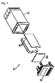
- Figs. 5 to 7 show exploded perspective views of the large-size, middle-size and small-size temperature regulators 1A to 1C, respectively, which include the base substrates 23a to 23c and the module substrates 25 to be housed in the cases 4a to 4c, respectively.
- the electronic components to be mounted on the substrates are not illustrated.
- module substrates 25 include a substrate for temperature regulation which forms the input module 8, a substrate for power supply which forms the power-supply module 9, and substrates for output/communication which form the output/communication module 10.
- the small-size temperature regulator 1C shown in Fig. 7 shows an example where three module substrates 25 are attached to the base substrate 23c which forms the front module 7.
- module substrates 25 include a substrate for temperature regulation which forms the input module 8, a substrate for power supply which forms the power-supply module 9, and a substrate for output/communication which forms the output/communication module 10. These three substrates corresponding to the modules 8, 9 and 10 are fundamental.
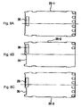
- a first module substrate 25-1 shown in Fig. 8A has an almost straight side which is the side having the connector 26; a second module substrate 25-2 shown in Fig. 8B has a cut portion 34 across half the length of the side having the connector 26; and a third module substrate 25-3 shown in Fig. 8C has a cut portion 35 with a shorter width than the cut portion 34 of the second module substrate 25-2.
- the first and third module substrates 25-1 and 25-3 place the connector 26 in the same position in the width direction of the side (vertical direction in the figure), and the second module substrate places the connector 26 in a different position.
- the electronic components mounted in the vicinity of the connectors 24 of the base substrates 23a to 23c are arranged in the necessary positions.
- misplacement of module substrates is prevented by combining the arrangement of electronic components in the vicinity of the connectors 24 of the base substrates 23a to 23c, the shapes of the sides of the module substrates 25 and the arrangement of the connectors 26 in the module substrate 25 in such a manner that the previously assigned module substrate 25 can be attached to the connector 24 of the base substrates 23a to 23c, but the non-assigned module substrates 25 cannot be attached. It is possible to prevent misplacement of module substrates by using different types of connectors having different numbers of pins from each other as the connectors 24 of the base substrates 23a to 23c and the connectors 26 of the module substrates 25, and by assigning the module substrates 25 more minutely to the base substrates 23a to 23c.
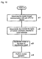
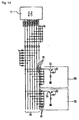
- the flowchart shown in Fig. 10 describes the control operation of the main CPU 17 of the temperature regulators 1A to 1C where a plurality of module substrates 25 forming the input module 8, the power- supplymodule 9, and the output/communication module 10 are attached to the base substrates 23a to 23c.
- Fig. 11 is a flowchart for describing the normal operation.
- step n5 it is determined whether the display communication flag indicative of a request for display process or communication process is on or not (step n5); when it is on, the display communication process is carried out (step n6); it is determined whether an HMI (Human Machine Interface) activation flag indicating whether there is a key operation and it is necessary to carry out the corresponding process (step n7); and when it is on, the HMI process corresponding to the key operation is carried out (step n8). Then, it is determined whether the control activation flag indicating whether the control process is necessary or not is on or not (step n9), and when it is on, a temperature regulation process is performed to return to step n5 (step n10)
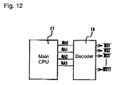
- the main CPU 17, as shown in Fig. 12. outputs 4-bit module address signals MA0 to MA3 to sequentially designate 11 connectors 24 at the maximum of the base substrate 23a to the decoder 16 shown in Fig. 2 of the base substrates 23a to 23c.
- the decoder 16 decodes the module address signals, and outputs reverse MS signals to designate any module corresponding to the 11 connectors 24.
- the further reversed MS signals turn on the transistors 37 of the corresponding module substrates 25 as shown in Fig. 13.
- Each module substrate 25 has a plurality of diodes 38 which are made conductive when the transistor 37 is turned on, and the number of the diodes 38 corresponds to the type of the module substrate 25.
- type signals TYPE0 to TYPE6 corresponding to the number of the diodes 38 of the module substrate 25 attached to the designated connector 24 are given to the main CPU 17 via the type bus 30, which makes the main CPU bus 17 identify the type of the module substrate 25 attached to the designated connector 24.
- the module substrates are discriminated to decide the model, thereby performing the corresponding control operation.
- the module substrates forming the input module, the power-supply module, and the output/communication module are shared among the large-size, middle-size and small-size temperature regulators 1A to 1C, as compared with the conventional example in which the module substrates are separately designed for each model, it becomes possible to reduce the cost by lowing the design cost, simplifying the assembly, and increasing the number of the same substrates to be mass-produced.
- Fig. 14 is an exploded perspective view of a digital panel mater as an electronic device according to another embodiment of the present invention.
- the digital panel meter 40 includes a case 45 formed of a front case 43 equipped with a display unit 41 for displaying a measurement value and the like and a plurality of operation keys 42, and a rear case 44.
- the case 45 houses a base substrate 46 and in this case three module substrates 25.
- Each module substrate 25 is provided with terminal stands 47 and a terminal cover 48 which covers the terminal stands 47.
- the base substrate 46 has a size specially designed for the digital panel meter 40, and includes five connectors 24 for attaching the module substrate 25 as shown in Fig. 15. In the diagonally shaded areas, five module substrates 25 at the maximum can be attached.
- the software for display of the digital panel meter 40 is made the same as the software for display of the temperature regulators 1A to 1C, and the main CPU of the input module 8 discriminates between different models such as between a temperature regulator and a digital panel meter as described above, and displays only the HMI necessary for the model.
- the main CPU discriminates between different models such as between a temperature regulator and a digital panel meter, and displays only the items (parameters) necessary for the model, without displaying unnecessary Items, there is no increase in the number of set items to be displayed even when the software for display is shared among different models. This can facilitate the setting operation, and prevent setting mistakes.
- the module substrates 25 attached to the base substrate 46 form the input module 8, the power-supply module 9 and the output/communication module 10 shown in Fig. 2, and the power-supply module 9 and the output/communication module 10 are so designed to be able to share the module substrates of the temperature regulators 1A to 1C.
- the input module 8 includes a main CPU which controls the operation of each model of digital panel meter and an input circuit which is supplied with inputs from various sensors which are not shown, and is formed of a substrate for measurement process which is detachably attached to the base substrate 46 via connectors.
- This substrate for measurement process performs a measurement process as a digital panel meter, unlike the above-mentioned substrate for temperature regulation which performs a temperature regulation process.
- Fig. 16 is a flowchart for describing the normal operation of this digital panel meter 40.
- This normal operation is basically the same as the case of the temperature regulator of Fig. 11 except that a measurement process is carried out in place of a temperature regulation process.
- This digital panel meter 40 in the same manner as the conventional digital panel meters, displays measurement values and the like, and also provides an alarm output based on the results of comparison with the previously set comparison values.
- the temperature regulators 1A to 1C. can share the power-supply and output/communication module substrates. thereby realizing further cost reduction in design, fabrication and control of these models.
- the main CPU as a control circuit is installed in the input module; however, in another embodiment of the present invention the main CPU may be installed in the front module or another module.
- an additional module substrate with an optional function may be attached.
- the base substrate is arranged along the front surface of the case; however, it can be arranged in a position other than the front surface.
- the attaching substrates are attached to the connection parts provided in the base substrate; however, in another embodiment of the present invention, the connection parts can be provided, for example, in the substrate for connection instead of the base substrate and the shared wiring of the base substrate and the wiring of the attaching substrates can be connected via the substrate for connection.
Landscapes
- Engineering & Computer Science (AREA)
- Physics & Mathematics (AREA)
- General Physics & Mathematics (AREA)
- Automation & Control Theory (AREA)
- Microelectronics & Electronic Packaging (AREA)
- Combinations Of Printed Boards (AREA)
- Programmable Controllers (AREA)
Abstract
Description
Claims (16)
- An electronic device equipped with a plurality of substrates, comprising:a base substrate which has a connection part and shared wiring connected to the connection part;an attaching substrate which has a special circuit in accordance with a function thereof and which is attached to the connection part so as to connect the special circuit with the shared wiring; anda control circuit which is mounted on either the base substrate or the attaching substrate, and which is connected to the shared wiring, whereinthe control circuit discriminates the attaching substrate attached to the connection part of the base substrate, thereby making the electronic device operate as a required model out of a plurality of models.
- The electronic device according to claim 1, whereinthe connection part is a connector, andthe attaching substrate to be detachably attached to the connector is sharable among different models.
- The electronic device according to claim 1 or 2, further comprising:a case for housing the plurality of substrates, whereinthe plurality of models have the same size of case, the base substrate is shared among the plurality of models, and the control circuit is mounted on the attaching substrate.
- The electronic device according to claim 1 or 2, further comprising:a case for housing the plurality of substrates, whereinthe plurality of models include a model having a different size of case, and the attaching substrate has a size corresponding to the model having the smallest case.
- The electronic device according to claim 1 or 2, comprising:an attaching substrate for input, an attaching substrate for power supply, and an attaching substrate for output which are provided with an input circuit, a power-supply circuit, and an output circuit, respectively, as the special circuit.
- The electronic device according to claim 1 or 2, whereinthe connection part of the base substrate is assigned a necessary attaching substrate to be attached according to the model, andthe electronic device further comprises a erroneous attachment prevention means for allowing the necessary attaching substrate to be attached to the connection part while preventing an attaching substrate other than the necessary attaching substrate from being attached.
- The electronic device according to claim 6, whereinthe erroneous attachment prevention means prevents an attaching substrate other than the necessary attaching substrate from being attached by causing a side of the attaching substrate to bring into contact with an electronic component mounted on the base substrate or allows the necessary attaching substrate to be attached by not causing the contact.
- An electronic device equipped with a plurality of substrates, comprising:a base substrate which has a plurality of connectors and shared wiring connected to the connectors;a plurality of attaching substrates which have respective special circuits in accordance with functions thereof and which are detachably attached to the connectors so as to connect the special circuits with the shared wiring; anda control circuit which is mounted on either the base substrate or the attaching substrates, and which is connected to the shared wiring, whereinthe control circuit discriminates the attaching substrates attached to the connectors of the base substrate, thereby making the electronic device perform temperature regulating operation as a required model out of a plurality of models.
- An electronic device equipped with a plurality of substrates, comprising:a base substrate which has a plurality of connectors and shared wiring connected to the connectors;a plurality of attaching substrates which have respective special circuits in accordance with functions thereof and which are detachably attached to the connectors so as to connect the special circuits with the shared wiring; anda control circuit which is mounted on either the base substrate or the attaching substrates, and which is connected to the shared wiring, whereinthe control circuit discriminates the attaching substrates attached to the connectors of the base substrate, thereby making the electronic device perform measurement processing operation as a required model out of a plurality of models.
- The electronic device according to claim 8 or 9 further comprising:a case for housing the plurality of substrates, whereinthe base substrate is housed in the case along a front surface of the case and is provided with an operation part and a display part, andthe attaching substrates are shareable among different models.
- The electronic device according to claim 10, whereinthe plurality of attaching substrates include an attaching substrate which is sharable between the model performing the temperature regulating operation and the model performing the measurement processing operation, andthe control circuit which makes the model perform the temperature regulating operation and the control circuit which makes the model perform the measurement processing operation are mounted on different attaching substrates.
- The electronic device according to claim 10. whereinthe plurality of models include a model having a different size of case, and the attaching substrates have a size corresponding to the model having the smallest case.
- The electronic device according to claim 10, comprisingan attaching substrate for input, an attaching substrate for power supply, and an attaching substrate for output which are provided with an input circuit, a power-supply circuit, and an output circuit, respectively, as the special circuits.
- The electronic device according to claim 10, whereinthe connectors of the base substrate are assigned necessary attaching substrates to be attached according to the model, andthe electronic device further comprises erroneous attachment prevention means for allowing the necessary attaching substrates to be attached to the connectors while preventing attaching substrates other than the necessary attaching substrates from being attached.
- The electronic device of claim 14, whereinthe erroneous attachment prevention means prevents the attaching substrates other than the necessary attaching substrates from being attached by causing a side of each the attaching substrates to bring into contact with an electronic component mounted on the base substrate or allows the necessary attaching substrates to be attached by not causing the contact.
- A method for using an electronic device comprising:a base substrate which has a connection part and shared wiring connected to the connection part; an attaching substrate which has a special circuit in accordance with a function thereof and which is attached to the connection part so as to connect the special circuit with the shared wiring; and a control circuit which is mounted on either the base substrate or the attaching substrate, and which is connected to the shared wiring, the control circuit discriminating the attaching substrate attached to the connection part of the base substrate, thereby making the electronic device operate as a required model out of a plurality of models, the method comprising the steps of:selecting the attaching substrate from a plurality of attaching substrates having different functions from each other; andattaching the selected attaching substrate to the connection part of the base substrate so as to use the electronic device as the required model.
Applications Claiming Priority (2)
| Application Number | Priority Date | Filing Date | Title |
|---|---|---|---|
| JP2002144490A JP3584932B2 (en) | 2002-05-20 | 2002-05-20 | Electronics |
| JP2002144490 | 2002-05-20 |
Publications (3)
| Publication Number | Publication Date |
|---|---|
| EP1372366A2 true EP1372366A2 (en) | 2003-12-17 |
| EP1372366A3 EP1372366A3 (en) | 2006-06-21 |
| EP1372366B1 EP1372366B1 (en) | 2008-02-27 |
Family
ID=29561176
Family Applications (1)
| Application Number | Title | Priority Date | Filing Date |
|---|---|---|---|
| EP03011347A Expired - Lifetime EP1372366B1 (en) | 2002-05-20 | 2003-05-19 | Electronic device and method for using the same |
Country Status (7)
| Country | Link |
|---|---|
| US (1) | US7031168B2 (en) |
| EP (1) | EP1372366B1 (en) |
| JP (1) | JP3584932B2 (en) |
| KR (1) | KR100525245B1 (en) |
| CN (1) | CN1258699C (en) |
| DE (1) | DE60319304T2 (en) |
| TW (1) | TW588579B (en) |
Cited By (1)
| Publication number | Priority date | Publication date | Assignee | Title |
|---|---|---|---|---|
| WO2021116267A1 (en) * | 2019-12-10 | 2021-06-17 | Schenck Process Europe Gmbh | Processing apparatus for controlling, measuring and regulating |
Families Citing this family (14)
| Publication number | Priority date | Publication date | Assignee | Title |
|---|---|---|---|---|
| JP2004063299A (en) * | 2002-07-30 | 2004-02-26 | Omron Corp | Equipment terminal block structure |
| DE10256648A1 (en) * | 2002-12-03 | 2004-06-17 | Endress + Hauser Wetzer Gmbh + Co Kg | Signal processing unit for process automation technology for mounting on a top-hat rail |
| DE50308254D1 (en) * | 2003-01-03 | 2007-10-31 | Rohde & Schwarz | gauge |
| JP4144436B2 (en) * | 2003-06-02 | 2008-09-03 | セイコーエプソン株式会社 | Electro-optic module and electronic device |
| US20060255608A1 (en) * | 2005-04-25 | 2006-11-16 | Siemens Aktiengesellschaft | Arrangement of groups of electronic components in a vehicle cockpit |
| JP5055878B2 (en) * | 2006-08-01 | 2012-10-24 | タイガー魔法瓶株式会社 | Electric rice cooker |
| JP5194971B2 (en) * | 2008-04-09 | 2013-05-08 | パナソニック株式会社 | microwave |
| JP5093270B2 (en) * | 2010-03-12 | 2012-12-12 | オムロン株式会社 | Control equipment |
| CN102162670B (en) * | 2011-05-06 | 2013-10-23 | 山东大学 | A central air-conditioning split type network intelligent temperature controller |
| JP2016015100A (en) * | 2014-07-03 | 2016-01-28 | パナソニックIpマネジメント株式会社 | Communication apparatus and communication module |
| USD867304S1 (en) * | 2018-05-31 | 2019-11-19 | Kabushiki Kaisha Toshiba | Protection relays |
| USD915313S1 (en) * | 2018-10-15 | 2021-04-06 | Abb Schweiz Ag | Electronic device housing |
| USD1085027S1 (en) * | 2018-10-18 | 2025-07-22 | Abb Schweiz Ag | Human machine interface for protection relay |
| US11888255B2 (en) | 2019-07-15 | 2024-01-30 | Panduit Corp. | Single pair ethernet connector |
Family Cites Families (10)
| Publication number | Priority date | Publication date | Assignee | Title |
|---|---|---|---|---|
| DE3509405A1 (en) * | 1985-03-13 | 1986-09-18 | Siemens AG, 1000 Berlin und 8000 München | ELECTRONIC DEVICE FOR CONTROL PANEL OR PANEL INSTALLATION WITH A SHEATH-LIKE HOUSING |
| JPH0599705A (en) * | 1991-10-11 | 1993-04-23 | Chino Corp | Recorder |
| US5428535A (en) * | 1992-09-17 | 1995-06-27 | Kansei Corporation | Vehicle control unit structure |
| US5339219A (en) * | 1993-04-05 | 1994-08-16 | Alex Urich | Modulated electronic breadboard |
| JPH0818258A (en) * | 1994-06-27 | 1996-01-19 | Matsushita Electric Ind Co Ltd | Preventing incorrect insertion of printed circuit board |
| JPH0920469A (en) * | 1995-07-04 | 1997-01-21 | Hitachi Ltd | Elevator control device |
| JPH10170311A (en) * | 1996-12-12 | 1998-06-26 | Nippon Seiki Co Ltd | Vehicle instrumentation |
| US6038138A (en) * | 1998-02-18 | 2000-03-14 | Nvision, Inc. | Connection arrangement for electronic equipment to provide functional expansion in at least one dimension |
| US6253266B1 (en) * | 1999-02-19 | 2001-06-26 | Inet Technologies, Inc. | Apparatus and method for controlling information flow in a card cage having multiple backplanes |
| US6268991B1 (en) * | 1999-06-25 | 2001-07-31 | General Electric Company | Method and arrangement for customizing electronic circuit interrupters |
-
2002
- 2002-05-20 JP JP2002144490A patent/JP3584932B2/en not_active Expired - Lifetime
-
2003
- 2003-05-14 CN CNB031313698A patent/CN1258699C/en not_active Expired - Lifetime
- 2003-05-15 US US10/438,333 patent/US7031168B2/en not_active Expired - Lifetime
- 2003-05-15 KR KR10-2003-0030887A patent/KR100525245B1/en not_active Expired - Fee Related
- 2003-05-19 EP EP03011347A patent/EP1372366B1/en not_active Expired - Lifetime
- 2003-05-19 TW TW092113417A patent/TW588579B/en not_active IP Right Cessation
- 2003-05-19 DE DE60319304T patent/DE60319304T2/en not_active Expired - Lifetime
Cited By (2)
| Publication number | Priority date | Publication date | Assignee | Title |
|---|---|---|---|---|
| WO2021116267A1 (en) * | 2019-12-10 | 2021-06-17 | Schenck Process Europe Gmbh | Processing apparatus for controlling, measuring and regulating |
| US12563678B2 (en) | 2019-12-10 | 2026-02-24 | Qlar Europe Gmbh | Processing apparatus for controlling, measuring and regulating |
Also Published As
| Publication number | Publication date |
|---|---|
| TW588579B (en) | 2004-05-21 |
| CN1258699C (en) | 2006-06-07 |
| EP1372366B1 (en) | 2008-02-27 |
| CN1460909A (en) | 2003-12-10 |
| JP2003338674A (en) | 2003-11-28 |
| US20040008492A1 (en) | 2004-01-15 |
| JP3584932B2 (en) | 2004-11-04 |
| KR100525245B1 (en) | 2005-10-31 |
| DE60319304T2 (en) | 2009-02-19 |
| EP1372366A3 (en) | 2006-06-21 |
| US7031168B2 (en) | 2006-04-18 |
| TW200403017A (en) | 2004-02-16 |
| KR20030090511A (en) | 2003-11-28 |
| DE60319304D1 (en) | 2008-04-10 |
Similar Documents
| Publication | Publication Date | Title |
|---|---|---|
| US7031168B2 (en) | Electronic component and the method of using it | |
| US7978465B2 (en) | Function expanding method for small-sized display device | |
| US4180860A (en) | Display station having universal module for interface with different single loop controllers | |
| US20070173960A1 (en) | Compact modular programmable logic controller | |
| EP1703347B1 (en) | Programmable logic controller device and programmable logic controller system | |
| KR100596919B1 (en) | Misconnection judging method and Electronic Equipment | |
| US5398711A (en) | Modular fluid characteristic sensor and additive controller | |
| KR20050084397A (en) | Process-oriented board with modular spc integration and expansion | |
| US5642290A (en) | Expansion chassis for a voltage regulator controller | |
| US5315071A (en) | Line branching printed circuit board for a computer numerical controller | |
| JP2853128B2 (en) | Control electronics | |
| US10108216B2 (en) | Power tap with adjustable configuration | |
| JPH1078806A (en) | Programmable display device | |
| JP2004030528A (en) | Module identification method and electronic device | |
| CN214850884U (en) | Integrated motor | |
| JP2004280373A (en) | Electronics | |
| JPH09179606A (en) | Servo control device | |
| EP4086639A1 (en) | Electrical indicator and method for displaying an electrical value using a digital display | |
| JPH07110703A (en) | Functional circuit block mechanism | |
| Controls | Operator Interface | |
| KR19990067322A (en) | Meter drive | |
| JPH10267699A (en) | Vehicle instrumentation | |
| JP3355301B2 (en) | Remote I/O Devices | |
| JPH03136115A (en) | Data processor | |
| JPH0535302A (en) | Control device |
Legal Events
| Date | Code | Title | Description |
|---|---|---|---|
| PUAI | Public reference made under article 153(3) epc to a published international application that has entered the european phase |
Free format text: ORIGINAL CODE: 0009012 |
|
| AK | Designated contracting states |
Kind code of ref document: A2 Designated state(s): AT BE BG CH CY CZ DE DK EE ES FI FR GB GR HU IE IT LI LU MC NL PT RO SE SI SK TR |
|
| AX | Request for extension of the european patent |
Extension state: AL LT LV MK |
|
| PUAL | Search report despatched |
Free format text: ORIGINAL CODE: 0009013 |
|
| AK | Designated contracting states |
Kind code of ref document: A3 Designated state(s): AT BE BG CH CY CZ DE DK EE ES FI FR GB GR HU IE IT LI LU MC NL PT RO SE SI SK TR |
|
| AX | Request for extension of the european patent |
Extension state: AL LT LV MK |
|
| RIC1 | Information provided on ipc code assigned before grant |
Ipc: G05B 19/042 20060101AFI20060512BHEP Ipc: H05K 7/14 20060101ALI20060512BHEP |
|
| RIN1 | Information on inventor provided before grant (corrected) |
Inventor name: KIDO, MSAKAZU,801, MINAMIFUDODO-CHO Inventor name: YONEDA, GEN,801, MINAMIFUDODO-CHO Inventor name: KATO, SHIGEYUKI,801, MINAMIFUDODO-CHO Inventor name: TAKAISHI, AKIRA,801, MINAMIFUDODO-CHO Inventor name: SURGA, TOSHIMICHI,801, MINAMIFUDODO-CHO Inventor name: NAGAMI, YOSHIHIRO,801, MINAMIFUDODO-CHO Inventor name: HOSOKAWA, HIROFUMI,801, MINAMIFUDODO-CHO Inventor name: MUKAI, ATSUSHI,801, MINAMIFUDODO-CHO Inventor name: KISHI, TAKAFUMI,801, MINAMIFUDODO-CHO |
|
| 17P | Request for examination filed |
Effective date: 20061214 |
|
| AKX | Designation fees paid |
Designated state(s): DE FR GB IT |
|
| 17Q | First examination report despatched |
Effective date: 20070216 |
|
| GRAP | Despatch of communication of intention to grant a patent |
Free format text: ORIGINAL CODE: EPIDOSNIGR1 |
|
| GRAS | Grant fee paid |
Free format text: ORIGINAL CODE: EPIDOSNIGR3 |
|
| GRAA | (expected) grant |
Free format text: ORIGINAL CODE: 0009210 |
|
| AK | Designated contracting states |
Kind code of ref document: B1 Designated state(s): DE FR GB IT |
|
| REG | Reference to a national code |
Ref country code: GB Ref legal event code: FG4D |
|
| REF | Corresponds to: |
Ref document number: 60319304 Country of ref document: DE Date of ref document: 20080410 Kind code of ref document: P |
|
| ET | Fr: translation filed | ||
| PLBE | No opposition filed within time limit |
Free format text: ORIGINAL CODE: 0009261 |
|
| STAA | Information on the status of an ep patent application or granted ep patent |
Free format text: STATUS: NO OPPOSITION FILED WITHIN TIME LIMIT |
|
| 26N | No opposition filed |
Effective date: 20081128 |
|
| REG | Reference to a national code |
Ref country code: DE Ref legal event code: R082 Ref document number: 60319304 Country of ref document: DE Representative=s name: KILIAN KILIAN & PARTNER MBB PATENTANWAELTE, DE Ref country code: DE Ref legal event code: R082 Ref document number: 60319304 Country of ref document: DE Representative=s name: KILIAN KILIAN & PARTNER, DE |
|
| REG | Reference to a national code |
Ref country code: FR Ref legal event code: PLFP Year of fee payment: 14 |
|
| REG | Reference to a national code |
Ref country code: FR Ref legal event code: PLFP Year of fee payment: 15 |
|
| REG | Reference to a national code |
Ref country code: FR Ref legal event code: PLFP Year of fee payment: 16 |
|
| PGFP | Annual fee paid to national office [announced via postgrant information from national office to epo] |
Ref country code: IT Payment date: 20220412 Year of fee payment: 20 Ref country code: GB Payment date: 20220401 Year of fee payment: 20 Ref country code: FR Payment date: 20220408 Year of fee payment: 20 Ref country code: DE Payment date: 20220329 Year of fee payment: 20 |
|
| REG | Reference to a national code |
Ref country code: DE Ref legal event code: R071 Ref document number: 60319304 Country of ref document: DE |
|
| REG | Reference to a national code |
Ref country code: GB Ref legal event code: PE20 Expiry date: 20230518 |
|
| PG25 | Lapsed in a contracting state [announced via postgrant information from national office to epo] |
Ref country code: GB Free format text: LAPSE BECAUSE OF EXPIRATION OF PROTECTION Effective date: 20230518 |