EP1371747A1 - Zns-sio 2 sputtering target and optical recording medium having zns-sio 2 phase-change type optical disc protective film formed through use of that target - Google Patents
Zns-sio 2 sputtering target and optical recording medium having zns-sio 2 phase-change type optical disc protective film formed through use of that target Download PDFInfo
- Publication number
- EP1371747A1 EP1371747A1 EP01273953A EP01273953A EP1371747A1 EP 1371747 A1 EP1371747 A1 EP 1371747A1 EP 01273953 A EP01273953 A EP 01273953A EP 01273953 A EP01273953 A EP 01273953A EP 1371747 A1 EP1371747 A1 EP 1371747A1
- Authority
- EP
- European Patent Office
- Prior art keywords
- sio
- zns
- target
- sputtering target
- powder
- Prior art date
- Legal status (The legal status is an assumption and is not a legal conclusion. Google has not performed a legal analysis and makes no representation as to the accuracy of the status listed.)
- Withdrawn
Links
Images
Classifications
-
- G—PHYSICS
- G11—INFORMATION STORAGE
- G11B—INFORMATION STORAGE BASED ON RELATIVE MOVEMENT BETWEEN RECORD CARRIER AND TRANSDUCER
- G11B7/00—Recording or reproducing by optical means, e.g. recording using a thermal beam of optical radiation by modifying optical properties or the physical structure, reproducing using an optical beam at lower power by sensing optical properties; Record carriers therefor
- G11B7/24—Record carriers characterised by shape, structure or physical properties, or by the selection of the material
- G11B7/241—Record carriers characterised by shape, structure or physical properties, or by the selection of the material characterised by the selection of the material
- G11B7/252—Record carriers characterised by shape, structure or physical properties, or by the selection of the material characterised by the selection of the material of layers other than recording layers
- G11B7/257—Record carriers characterised by shape, structure or physical properties, or by the selection of the material characterised by the selection of the material of layers other than recording layers of layers having properties involved in recording or reproduction, e.g. optical interference layers or sensitising layers or dielectric layers, which are protecting the recording layers
- G11B7/2578—Record carriers characterised by shape, structure or physical properties, or by the selection of the material characterised by the selection of the material of layers other than recording layers of layers having properties involved in recording or reproduction, e.g. optical interference layers or sensitising layers or dielectric layers, which are protecting the recording layers consisting essentially of inorganic materials
-
- C—CHEMISTRY; METALLURGY
- C23—COATING METALLIC MATERIAL; COATING MATERIAL WITH METALLIC MATERIAL; CHEMICAL SURFACE TREATMENT; DIFFUSION TREATMENT OF METALLIC MATERIAL; COATING BY VACUUM EVAPORATION, BY SPUTTERING, BY ION IMPLANTATION OR BY CHEMICAL VAPOUR DEPOSITION, IN GENERAL; INHIBITING CORROSION OF METALLIC MATERIAL OR INCRUSTATION IN GENERAL
- C23C—COATING METALLIC MATERIAL; COATING MATERIAL WITH METALLIC MATERIAL; SURFACE TREATMENT OF METALLIC MATERIAL BY DIFFUSION INTO THE SURFACE, BY CHEMICAL CONVERSION OR SUBSTITUTION; COATING BY VACUUM EVAPORATION, BY SPUTTERING, BY ION IMPLANTATION OR BY CHEMICAL VAPOUR DEPOSITION, IN GENERAL
- C23C14/00—Coating by vacuum evaporation, by sputtering or by ion implantation of the coating forming material
- C23C14/06—Coating by vacuum evaporation, by sputtering or by ion implantation of the coating forming material characterised by the coating material
-
- C—CHEMISTRY; METALLURGY
- C23—COATING METALLIC MATERIAL; COATING MATERIAL WITH METALLIC MATERIAL; CHEMICAL SURFACE TREATMENT; DIFFUSION TREATMENT OF METALLIC MATERIAL; COATING BY VACUUM EVAPORATION, BY SPUTTERING, BY ION IMPLANTATION OR BY CHEMICAL VAPOUR DEPOSITION, IN GENERAL; INHIBITING CORROSION OF METALLIC MATERIAL OR INCRUSTATION IN GENERAL
- C23C—COATING METALLIC MATERIAL; COATING MATERIAL WITH METALLIC MATERIAL; SURFACE TREATMENT OF METALLIC MATERIAL BY DIFFUSION INTO THE SURFACE, BY CHEMICAL CONVERSION OR SUBSTITUTION; COATING BY VACUUM EVAPORATION, BY SPUTTERING, BY ION IMPLANTATION OR BY CHEMICAL VAPOUR DEPOSITION, IN GENERAL
- C23C14/00—Coating by vacuum evaporation, by sputtering or by ion implantation of the coating forming material
- C23C14/22—Coating by vacuum evaporation, by sputtering or by ion implantation of the coating forming material characterised by the process of coating
- C23C14/34—Sputtering
- C23C14/3407—Cathode assembly for sputtering apparatus, e.g. Target
- C23C14/3414—Metallurgical or chemical aspects of target preparation, e.g. casting, powder metallurgy
-
- G—PHYSICS
- G11—INFORMATION STORAGE
- G11B—INFORMATION STORAGE BASED ON RELATIVE MOVEMENT BETWEEN RECORD CARRIER AND TRANSDUCER
- G11B7/00—Recording or reproducing by optical means, e.g. recording using a thermal beam of optical radiation by modifying optical properties or the physical structure, reproducing using an optical beam at lower power by sensing optical properties; Record carriers therefor
- G11B7/24—Record carriers characterised by shape, structure or physical properties, or by the selection of the material
- G11B7/241—Record carriers characterised by shape, structure or physical properties, or by the selection of the material characterised by the selection of the material
- G11B7/252—Record carriers characterised by shape, structure or physical properties, or by the selection of the material characterised by the selection of the material of layers other than recording layers
- G11B7/254—Record carriers characterised by shape, structure or physical properties, or by the selection of the material characterised by the selection of the material of layers other than recording layers of protective topcoat layers
-
- G—PHYSICS
- G11—INFORMATION STORAGE
- G11B—INFORMATION STORAGE BASED ON RELATIVE MOVEMENT BETWEEN RECORD CARRIER AND TRANSDUCER
- G11B7/00—Recording or reproducing by optical means, e.g. recording using a thermal beam of optical radiation by modifying optical properties or the physical structure, reproducing using an optical beam at lower power by sensing optical properties; Record carriers therefor
- G11B7/24—Record carriers characterised by shape, structure or physical properties, or by the selection of the material
- G11B7/26—Apparatus or processes specially adapted for the manufacture of record carriers
-
- G—PHYSICS
- G11—INFORMATION STORAGE
- G11B—INFORMATION STORAGE BASED ON RELATIVE MOVEMENT BETWEEN RECORD CARRIER AND TRANSDUCER
- G11B7/00—Recording or reproducing by optical means, e.g. recording using a thermal beam of optical radiation by modifying optical properties or the physical structure, reproducing using an optical beam at lower power by sensing optical properties; Record carriers therefor
- G11B7/24—Record carriers characterised by shape, structure or physical properties, or by the selection of the material
- G11B7/241—Record carriers characterised by shape, structure or physical properties, or by the selection of the material characterised by the selection of the material
- G11B7/252—Record carriers characterised by shape, structure or physical properties, or by the selection of the material characterised by the selection of the material of layers other than recording layers
- G11B7/257—Record carriers characterised by shape, structure or physical properties, or by the selection of the material characterised by the selection of the material of layers other than recording layers of layers having properties involved in recording or reproduction, e.g. optical interference layers or sensitising layers or dielectric layers, which are protecting the recording layers
- G11B2007/25705—Record carriers characterised by shape, structure or physical properties, or by the selection of the material characterised by the selection of the material of layers other than recording layers of layers having properties involved in recording or reproduction, e.g. optical interference layers or sensitising layers or dielectric layers, which are protecting the recording layers consisting essentially of inorganic materials
- G11B2007/25706—Record carriers characterised by shape, structure or physical properties, or by the selection of the material characterised by the selection of the material of layers other than recording layers of layers having properties involved in recording or reproduction, e.g. optical interference layers or sensitising layers or dielectric layers, which are protecting the recording layers consisting essentially of inorganic materials containing transition metal elements (Zn, Fe, Co, Ni, Pt)
-
- G—PHYSICS
- G11—INFORMATION STORAGE
- G11B—INFORMATION STORAGE BASED ON RELATIVE MOVEMENT BETWEEN RECORD CARRIER AND TRANSDUCER
- G11B7/00—Recording or reproducing by optical means, e.g. recording using a thermal beam of optical radiation by modifying optical properties or the physical structure, reproducing using an optical beam at lower power by sensing optical properties; Record carriers therefor
- G11B7/24—Record carriers characterised by shape, structure or physical properties, or by the selection of the material
- G11B7/241—Record carriers characterised by shape, structure or physical properties, or by the selection of the material characterised by the selection of the material
- G11B7/252—Record carriers characterised by shape, structure or physical properties, or by the selection of the material characterised by the selection of the material of layers other than recording layers
- G11B7/257—Record carriers characterised by shape, structure or physical properties, or by the selection of the material characterised by the selection of the material of layers other than recording layers of layers having properties involved in recording or reproduction, e.g. optical interference layers or sensitising layers or dielectric layers, which are protecting the recording layers
- G11B2007/25705—Record carriers characterised by shape, structure or physical properties, or by the selection of the material characterised by the selection of the material of layers other than recording layers of layers having properties involved in recording or reproduction, e.g. optical interference layers or sensitising layers or dielectric layers, which are protecting the recording layers consisting essentially of inorganic materials
- G11B2007/2571—Record carriers characterised by shape, structure or physical properties, or by the selection of the material characterised by the selection of the material of layers other than recording layers of layers having properties involved in recording or reproduction, e.g. optical interference layers or sensitising layers or dielectric layers, which are protecting the recording layers consisting essentially of inorganic materials containing group 14 elements except carbon (Si, Ge, Sn, Pb)
-
- G—PHYSICS
- G11—INFORMATION STORAGE
- G11B—INFORMATION STORAGE BASED ON RELATIVE MOVEMENT BETWEEN RECORD CARRIER AND TRANSDUCER
- G11B7/00—Recording or reproducing by optical means, e.g. recording using a thermal beam of optical radiation by modifying optical properties or the physical structure, reproducing using an optical beam at lower power by sensing optical properties; Record carriers therefor
- G11B7/24—Record carriers characterised by shape, structure or physical properties, or by the selection of the material
- G11B7/241—Record carriers characterised by shape, structure or physical properties, or by the selection of the material characterised by the selection of the material
- G11B7/252—Record carriers characterised by shape, structure or physical properties, or by the selection of the material characterised by the selection of the material of layers other than recording layers
- G11B7/257—Record carriers characterised by shape, structure or physical properties, or by the selection of the material characterised by the selection of the material of layers other than recording layers of layers having properties involved in recording or reproduction, e.g. optical interference layers or sensitising layers or dielectric layers, which are protecting the recording layers
- G11B2007/25705—Record carriers characterised by shape, structure or physical properties, or by the selection of the material characterised by the selection of the material of layers other than recording layers of layers having properties involved in recording or reproduction, e.g. optical interference layers or sensitising layers or dielectric layers, which are protecting the recording layers consisting essentially of inorganic materials
- G11B2007/25715—Record carriers characterised by shape, structure or physical properties, or by the selection of the material characterised by the selection of the material of layers other than recording layers of layers having properties involved in recording or reproduction, e.g. optical interference layers or sensitising layers or dielectric layers, which are protecting the recording layers consisting essentially of inorganic materials containing oxygen
-
- G—PHYSICS
- G11—INFORMATION STORAGE
- G11B—INFORMATION STORAGE BASED ON RELATIVE MOVEMENT BETWEEN RECORD CARRIER AND TRANSDUCER
- G11B7/00—Recording or reproducing by optical means, e.g. recording using a thermal beam of optical radiation by modifying optical properties or the physical structure, reproducing using an optical beam at lower power by sensing optical properties; Record carriers therefor
- G11B7/24—Record carriers characterised by shape, structure or physical properties, or by the selection of the material
- G11B7/241—Record carriers characterised by shape, structure or physical properties, or by the selection of the material characterised by the selection of the material
- G11B7/252—Record carriers characterised by shape, structure or physical properties, or by the selection of the material characterised by the selection of the material of layers other than recording layers
- G11B7/257—Record carriers characterised by shape, structure or physical properties, or by the selection of the material characterised by the selection of the material of layers other than recording layers of layers having properties involved in recording or reproduction, e.g. optical interference layers or sensitising layers or dielectric layers, which are protecting the recording layers
- G11B2007/25705—Record carriers characterised by shape, structure or physical properties, or by the selection of the material characterised by the selection of the material of layers other than recording layers of layers having properties involved in recording or reproduction, e.g. optical interference layers or sensitising layers or dielectric layers, which are protecting the recording layers consisting essentially of inorganic materials
- G11B2007/25716—Record carriers characterised by shape, structure or physical properties, or by the selection of the material characterised by the selection of the material of layers other than recording layers of layers having properties involved in recording or reproduction, e.g. optical interference layers or sensitising layers or dielectric layers, which are protecting the recording layers consisting essentially of inorganic materials containing sulfur
-
- G—PHYSICS
- G11—INFORMATION STORAGE
- G11B—INFORMATION STORAGE BASED ON RELATIVE MOVEMENT BETWEEN RECORD CARRIER AND TRANSDUCER
- G11B7/00—Recording or reproducing by optical means, e.g. recording using a thermal beam of optical radiation by modifying optical properties or the physical structure, reproducing using an optical beam at lower power by sensing optical properties; Record carriers therefor
- G11B7/24—Record carriers characterised by shape, structure or physical properties, or by the selection of the material
- G11B7/241—Record carriers characterised by shape, structure or physical properties, or by the selection of the material characterised by the selection of the material
- G11B7/252—Record carriers characterised by shape, structure or physical properties, or by the selection of the material characterised by the selection of the material of layers other than recording layers
- G11B7/258—Record carriers characterised by shape, structure or physical properties, or by the selection of the material characterised by the selection of the material of layers other than recording layers of reflective layers
- G11B7/2585—Record carriers characterised by shape, structure or physical properties, or by the selection of the material characterised by the selection of the material of layers other than recording layers of reflective layers based on aluminium
Definitions
- the present invention relates particularly to a ZnS-SiO 2 sputtering target effective in forming a ZnS-SiO 2 phase change optical disc protective film capable of reducing particles (raising dust) and nodules generated at the time of sputtering upon forming a film with sputtering, and improving the productivity of high-density products without much variation in the quality, as well as to an optical recording medium having formed thereon the ZnS-SiO 2 phase change optical disc protective film using such a target.
- phase change optical disc In recent years, high-density recordable optical disc technology capable of recording/playing without requiring a magnetic head has been developed, and is rapidly attracting attention.
- This optical disc can be classified into the three categories of read-only, write-once and rewritable. Particularly, the phase change method employed in the write-once and rewritable type discs is attracting attention.
- the fundamental principle of the recording/ playing employing this phase change optical disc is briefly described below.
- This phase change optical disc performs the recording/ playing of information by heating and increasing the temperature of a recording thin film on a substrate by irradiating a laser beam thereto, and generating a crystallographic phase change (amorphous ⁇ crystal) in the structure of such recording thin film. More specifically, the playing of information is conducted by detecting the change in the reflectivity caused by the change in the optical constant of the phase.
- the aforementioned phase change is performed with the irradiation of a laser beam narrowed down to a diameter of approximately 1 to several ⁇ m.
- a 1 ⁇ m laser beam passes through at a linear velocity of 10m/s, light is irradiated to a certain point on the optical disc for 100ns, and it is necessary to perform the aforementioned phase change and detect the reflectivity within such time frame.
- the peripheral dielectric protective layer and aluminum alloy reflective layer will also be repeatedly adject thereto.
- a phase change optical disc has a four-layer structure wherein, for instance, both sides of a Ge-Sb-Te recording thin film layer are sandwiched with a protective layer of ZnS-SiO 2 high-melting point dielectric, and an aluminum alloy reflective layer is additionally provided thereto.
- the reflective layer and protective layer are also demanded of a function for preventing the deformation caused by the moisture resistance or heat of the recording thin film as well as a function for controlling the thermal conditions upon recording (c.f. "Kogaku" magazine, volume 26, no. 1, pages 9 to 15).
- the protective layer of a high-melting point dielectric must be durable against repeated thermal stress caused by the heating and cooling, must not allow such thermal effect to influence the reflective film or other areas, and it is also required to be thin, of low reflectivity, and possess strength to prevent deterioration. From this perspective, the dielectric protective layer plays an important role.
- the dielectric protective layer described above is usually formed with the sputtering method.
- This sputtering method makes a positive electrode target and a negative electrode target face each other, and generates an electric field by applying a high voltage between the substrates thereof and the targets under an inert gas atmosphere.
- the sputtering method employs a fundamental principle where plasma is formed pursuant to the collision of electrons, which are ionized at such time, and the inert gas, the positive ion in this plasma extrudes the target structured atoms by colliding with the target (negative electrode) surface, and the extruded atoms adhere to the opposing substrate surface.
- sputtering is conducted with a ceramic target such as ZnS-SiO 2 in order to form a thin film of approximately 1000 to 2000 ⁇ .
- These materials are deposited with a high-frequency sputtering (RF) device, a magnetron-sputtering device, or with a DC (direct current) sputtering device upon conducting special processing to the target material.
- RF high-frequency sputtering
- magnetron-sputtering device magnetron-sputtering device
- DC (direct current) sputtering device upon conducting special processing to the target material.
- the sputtering face of the target can be made even and smooth by miniaturizing and highly densifying the crystal grain of the ZnS-SiO 2 target, whereby yielding a characteristic of reducing particles and nodules as well as prolonging the target life. It is well known that the productivity of optical discs can be improved as a result thereof.
- SiO 2 used in a conventional ZnS-SiO 2 target employed were those having a high purity of 4N or more and having an average grain diameter of 0.1 to 20 ⁇ m, and are ordinarily manufactured by being sintered between 800 and 1200°C. With this temperature range, however, the SiO 2 itself will not deform or react with ZnS.
- a ZnS-SiO 2 target manufactured as above easily creates a space between the ZnS and SiO 2 , which becomes more noticeable when the SiO 2 is miniaturized, and, since the precision of the ZnS is also hindered thereby, there is a problem in that the target density will deteriorate.
- the hot pressing device may be enlarged in order to enlarge the graphite mold itself, this will lead to increased costs for such hot pressing device and graphite mold.
- An object of the present invention is to enable the stable manufacture of a target at low cost and in which the crystal grain is minute and of a high density of 90% or more, and to thereby obtain a sputtering target for forming an optical disc protective film capable of further improving the evenness of deposition and increasing the productivity rate, and an optical recording medium having formed thereon a ZnS-SiO 2 phase change optical disc protective film upon employing the ZnS-SiO 2 sputtering target.
- the present inventors discovered that by employing a SiO 2 glass material in which an additive is added to the SiO 2 , space between the ZnS can be reduced, high densification can be easily realized even upon miniaturizing the SiO 2 , generation of particles and nodules arising at the time of sputtering can be reduced without detriment to the characteristics as a protective film, and evenness of the film thickness can also be improved.
- the present invention provides:
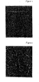
- Fig. 1 is a microphotograph of the target surface obtained pursuant to Example 1;
- Fig. 2 is a microphotograph of the target surface obtained pursuant to Example 2; and
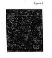
- Fig. 3 is a microphotograph of the target surface obtained in Comparative Example 1.
- the present invention employs SiO 2 glass powder containing, as an additive, a total of 0.01 to 20wt% of one or more types selected from a metal element, boron, phosphorus, arsenic or the oxides thereof.
- a metal element in particular, it is desirable to use lithium, sodium, magnesium, aluminum, potassium, calcium, barium, or lead.
- a significant characteristic of the present invention is to use SiO 2 glass material.
- the additive Since the additive will be ineffective if the additive amount of the additive is less than 0.01wt%, and the film characteristics will change largely, which is not preferable, if the additive amount exceeds 20wt%, the total amount has been set between 0.01 and 20wt%.
- the target is manufactured by evenly dispersing and mixing to 50mol% of the SiO 2 glass powder containing the foregoing additive elements and the remnant ZnS powder, and sintering this with hot pressing or the like.
- SiO 2 powder it is further possible to add 0.01 to 30mol% of SiO 2 powder to the foregoing SiO 2 glass powder, evenly dispersing and mixing this with the remnant ZnS powder, and sintering this with hot pressing or the like.
- the additive amount of the foregoing metal element may be reduced in accordance with the purpose of use, and high densification is possible even if the amount of SiO 2 composition is great.
- each of the additive materials is of high purity, and, for example, although those having 99.99wt% or more are employed, the additive materials are not necessarily limited to this range.
- Obtained thereby is a sputtering target for forming the ZnS-SiO 2 phase change optical disc protective film with not much space between the ZnS and SiO 2 , and which has a relative density of 90% or more.
- the ZnS-SiO 2 target crystal grain can be miniaturized and highly densified, and, therefore, yielded is a significant effect where the sputtering face of the target can be made even and smooth, particles and nodules at the time of sputtering can be reduced, and the target life can be prolonged.
- the productivity of the optical recording medium having formed thereon a ZnS-SiO 2 phase change optical disc protective film will increase, and a material superior in quality can be obtained thereby.
- SiO 2 glass powder having as its constitutional composition SiO 2 -0.5 wt% Na 2 O was evenly mixed with ZnS at a ratio of 20mol%.
- This mixed powder was filled in a graphite die, and hot pressed under the conditions of an Ar atmosphere, a bearing of 150kg/cm 2 , and a temperature of 1000°C.
- the target obtained thereby had a relative density of 99%.
- the microphotograph of the surface of this target is shown in Fig. 1.
- the black spherical shapes in Fig. 1 represent the SiO 2 , and the average grain diameter of the SiO 2 crystal grain was 5 ⁇ m or less, and space between the surfaces of ZnS and SiO 2 could hardly be acknowledged. As a result, obtained was a high-density sputtering target for forming a ZnS-SiO 2 phase change optical disc protective film.
- SiO 2 glass powder having as its constitutional composition SiO 2 -0.5wt% B 2 O 3 was evenly mixed with ZnS at a ratio of 20mol%.
- This mixed powder was filled in a graphite die, and hot pressed under the conditions of an Ar atmosphere, a bearing of 150kg/cm 2 , and a temperature of 1000°C.
- the target obtained thereby had a relative density of 97%.
- obtained was a high-density sputtering target for forming a ZnS-SiO 2 phase change optical disc protective film.
- the SEM photograph thereof is shown in Fig. 2.
- the black spherical shapes in Fig. 2 represent the SiO 2 , and the average grain diameter of the SiO 2 crystal grain was 10 ⁇ m or less, and it is evident that the space between the surfaces of ZnS and SiO 2 is minimal.
- SiO 2 powder having a purity of 99.99% or higher was evenly mixed with ZnS at a ratio of 20mol%.
- This mixed powder was filled in a graphite die, and hot pressed under the conditions of an Ar atmosphere, a bearing of 150kg/cm 2 , and a temperature of 1000°C.
- the target obtained thereby had a relative density of 94%.
- obtained was a sputtering target for forming a ZnS-SiO 2 phase change optical disc protective film inferior to the density yielded in the Examples of the present invention.
- Fig. 3 The microphotograph of the surface of this target is shown in Fig. 3. Similar to the above, the black spherical shapes in Fig. 3 represent the SiO 2 , and many spaces between the surfaces of ZnS and SiO 2 could be acknowledged.
- the SiO 2 glass material of the present invention in which an additive was added to SiO 2 , space between the ZnS can be reduced, and high densification can be easily realized even upon miniaturizing the SiO 2 .
- a superior effect is yielded of being able to obtain a sputtering target for forming an optical disc protective film capable of suppressing the generation of particles (raising dust) and nodules arising at the time of sputtering without detriment to the characteristics as a protective film, improving the evenness of deposition and increasing the productivity rate, and an optical recording medium having formed thereon a ZnS-SiO 2 phase change optical disc protective film upon employing the ZnS-SiO 2 sputtering target.
Landscapes
- Chemical & Material Sciences (AREA)
- Engineering & Computer Science (AREA)
- Metallurgy (AREA)
- Organic Chemistry (AREA)
- Chemical Kinetics & Catalysis (AREA)
- Materials Engineering (AREA)
- Mechanical Engineering (AREA)
- Manufacturing & Machinery (AREA)
- Inorganic Chemistry (AREA)
- Manufacturing Optical Record Carriers (AREA)
- Physical Vapour Deposition (AREA)
- Optical Record Carriers And Manufacture Thereof (AREA)
- Compositions Of Oxide Ceramics (AREA)
Abstract
Description
Claims (5)
- A ZnS-SiO2 sputtering target having a relative density of 90% or more characterized in being sintered with powder wherein 1 to 50mol% of SiO2 glass powder containing, as an additive, a total of 0.01 to 20wt% of one or more types selected from a metal element, boron, phosphorus, arsenic or the oxides thereof, and the remnant ZnS powder are evenly dispersed and mixed.
- A ZnS-SiO2 sputtering target having a relative density of 90% or more characterized in being sintered with powder wherein 1 to 50mol% of SiO2 glass powder containing, as an additive, a total of 0.01 to 20wt% of one or more types selected from a metal element, boron, phosphorus, arsenic or the oxides thereof, 0.01 to 30mol% of SiO2 powder, and the remnant ZnS powder are evenly dispersed and mixed.
- A ZnS-SiO2 sputtering target according to claim 1 or claim 2, characterized in that the metal element is lithium, sodium, magnesium, aluminum, potassium, calcium, or barium.
- A ZnS-SiO2 sputtering target according to each of claims 1 to 3, characterized in that the average grain diameter of the SiO2 crystal grain is 0.1 to 30 µm.
- An optical recording medium having formed thereon a ZnS-SiO2 phase change optical disc protective film upon employing the ZnS-SiO2 sputtering target according to each of claims 1 to 4.
Applications Claiming Priority (3)
| Application Number | Priority Date | Filing Date | Title |
|---|---|---|---|
| JP2001068317 | 2001-03-12 | ||
| JP2001068317A JP3916125B2 (en) | 2001-03-12 | 2001-03-12 | ZnS-SiO2 sputtering target and optical recording medium on which a ZnS-SiO2 phase change optical disk protective film is formed using the target |
| PCT/JP2001/010509 WO2002072910A1 (en) | 2001-03-12 | 2001-11-30 | Zns-sio2 sputtering target and optical recording medium having zns-sio2 phase-change type optical disc protective film formed through use of that target |
Publications (2)
| Publication Number | Publication Date |
|---|---|
| EP1371747A1 true EP1371747A1 (en) | 2003-12-17 |
| EP1371747A4 EP1371747A4 (en) | 2008-08-20 |
Family
ID=18926526
Family Applications (1)
| Application Number | Title | Priority Date | Filing Date |
|---|---|---|---|
| EP01273953A Withdrawn EP1371747A4 (en) | 2001-03-12 | 2001-11-30 | ZNS-SIO2 SPRAY TARGET AND OPTICAL RECORDING MEDIUM WITH PHASE CHANGE TYPE ZNS-SIO2 OPTICAL DISK PROTECTION MEDIA ESTABLISHED THROUGH THIS TARGET |
Country Status (5)
| Country | Link |
|---|---|
| EP (1) | EP1371747A4 (en) |
| JP (1) | JP3916125B2 (en) |
| CN (1) | CN1235213C (en) |
| TW (1) | TWI237668B (en) |
| WO (1) | WO2002072910A1 (en) |
Cited By (3)
| Publication number | Priority date | Publication date | Assignee | Title |
|---|---|---|---|---|
| EP1380670A4 (en) * | 2001-04-13 | 2007-07-18 | Nippon Mining Co | ZNS-SIO2 CATHODIC SPUTTER TARGET AND OPTICAL RECORDING MEDIUM HAVING ZNS-SIO2 PROTECTIVE LAYER FOR OPTICAL PHASE TRANSITION DISK FORMED THEREFROM |
| EP1394284A4 (en) * | 2001-06-01 | 2008-08-20 | Nippon Mining Co | SPRAY TARGET FOR CREATING A PHASE MODIFICATION OPTICAL DISK PROTECTIVE FILM AND OPTICAL RECORDING MEDIUM HAVING THE PROTECTIVE FILM OBTAINED USING THE SAME |
| WO2009132726A1 (en) * | 2008-04-18 | 2009-11-05 | Sony Dadc Austria Ag | Method for manufacturing an optical waveguide, optical waveguide, and sensor arrangement |
Families Citing this family (1)
| Publication number | Priority date | Publication date | Assignee | Title |
|---|---|---|---|---|
| JP5019343B2 (en) * | 2004-01-27 | 2012-09-05 | Jx日鉱日石金属株式会社 | ZnS powder for sputtering target and sputtering target |
Family Cites Families (6)
| Publication number | Priority date | Publication date | Assignee | Title |
|---|---|---|---|---|
| JP4250686B2 (en) * | 1998-05-28 | 2009-04-08 | 東ソー株式会社 | Sputtering target |
| JP3358548B2 (en) * | 1998-07-21 | 2002-12-24 | 三菱マテリアル株式会社 | Sputtering target for optical recording medium protective film formation without spatter cracking |
| JP3533333B2 (en) * | 1998-08-21 | 2004-05-31 | Tdk株式会社 | Sputtering target for interference film of optical recording medium and method of manufacturing the same |
| JP3468136B2 (en) * | 1998-12-18 | 2003-11-17 | 三菱マテリアル株式会社 | Sputtering target for forming optical recording medium protective film |
| JP2001064766A (en) * | 1999-08-26 | 2001-03-13 | Mitsubishi Materials Corp | Sputtering target for optical recording protective film formation with less generation of particles |
| JP2001192819A (en) * | 2000-01-06 | 2001-07-17 | Mitsubishi Materials Corp | Sputtering target for optical recording protective film formation capable of DC sputtering |
-
2001
- 2001-03-12 JP JP2001068317A patent/JP3916125B2/en not_active Expired - Lifetime
- 2001-11-30 WO PCT/JP2001/010509 patent/WO2002072910A1/en not_active Ceased
- 2001-11-30 CN CN01822686.8A patent/CN1235213C/en not_active Expired - Lifetime
- 2001-11-30 EP EP01273953A patent/EP1371747A4/en not_active Withdrawn
-
2002
- 2002-03-04 TW TW091103902A patent/TWI237668B/en not_active IP Right Cessation
Cited By (4)
| Publication number | Priority date | Publication date | Assignee | Title |
|---|---|---|---|---|
| EP1380670A4 (en) * | 2001-04-13 | 2007-07-18 | Nippon Mining Co | ZNS-SIO2 CATHODIC SPUTTER TARGET AND OPTICAL RECORDING MEDIUM HAVING ZNS-SIO2 PROTECTIVE LAYER FOR OPTICAL PHASE TRANSITION DISK FORMED THEREFROM |
| EP1394284A4 (en) * | 2001-06-01 | 2008-08-20 | Nippon Mining Co | SPRAY TARGET FOR CREATING A PHASE MODIFICATION OPTICAL DISK PROTECTIVE FILM AND OPTICAL RECORDING MEDIUM HAVING THE PROTECTIVE FILM OBTAINED USING THE SAME |
| WO2009132726A1 (en) * | 2008-04-18 | 2009-11-05 | Sony Dadc Austria Ag | Method for manufacturing an optical waveguide, optical waveguide, and sensor arrangement |
| US8811790B2 (en) | 2008-04-18 | 2014-08-19 | Sony Dadc Austria Ag | Method for manufacturing an optical waveguide, optical waveguide, and sensor arrangement |
Also Published As
| Publication number | Publication date |
|---|---|
| TWI237668B (en) | 2005-08-11 |
| WO2002072910A1 (en) | 2002-09-19 |
| JP3916125B2 (en) | 2007-05-16 |
| JP2002266070A (en) | 2002-09-18 |
| EP1371747A4 (en) | 2008-08-20 |
| CN1533446A (en) | 2004-09-29 |
| CN1235213C (en) | 2006-01-04 |
Similar Documents
| Publication | Publication Date | Title |
|---|---|---|
| EP1475795B1 (en) | Sputtering target containing zinc sulfide as major component, optical recording medium on which phase change optical disk protective film containing zinc sulfide as major component is formed by using the target, and method for manufacturing the sputtering target | |
| JPWO2009078306A1 (en) | Thin film mainly composed of titanium oxide, sintered compact sputtering target suitable for production of thin film mainly composed of titanium oxide, and method for producing thin film mainly composed of titanium oxide | |
| EP1380670A1 (en) | Zns-sio2 sputtering target and optical recording medium having zns-sio2 protective film for phase change type optical disk formed by using said target | |
| EP1394284A1 (en) | Sputtering target for forming phase change optical disc protective film and optical recording medium having phase change optical disc protective film formed using that target | |
| KR100663616B1 (en) | Germanium-chromium alloy sputtering target and manufacturing method thereof | |
| JP3916125B2 (en) | ZnS-SiO2 sputtering target and optical recording medium on which a ZnS-SiO2 phase change optical disk protective film is formed using the target | |
| JP5080527B2 (en) | Sputtering target | |
| JP4817137B2 (en) | Sputtering target and optical recording medium | |
| JP2001011615A (en) | Sputtering target for forming protective film for optical disk | |
| JP4579224B2 (en) | Method of manufacturing sputtering target for forming phase change type optical disk protective film | |
| JP4279533B2 (en) | Sputtering target and optical recording medium | |
| JP4625050B2 (en) | ZnS-SiO2 sputtering target | |
| JP4807679B2 (en) | Powder for sintering sputtering target | |
| JP4685177B2 (en) | Sputtering target for forming phase change optical disc protective film and optical recording medium having phase change optical disc protective film formed using the target | |
| JP2005239532A (en) | ZnS POWDER FOR SPUTTERING TARGET, AND SPUTTERING TARGET | |
| JP2002266069A (en) | METHOD FOR MANUFACTURING ZnS-SiO2 SPUTTERING TARGET | |
| WO2003044241A1 (en) | Spattering target for use in forming preventive film for optical recording medium, method for preparing the target, and optical recording medium having preventive film formed by use of the target |
Legal Events
| Date | Code | Title | Description |
|---|---|---|---|
| PUAI | Public reference made under article 153(3) epc to a published international application that has entered the european phase |
Free format text: ORIGINAL CODE: 0009012 |
|
| 17P | Request for examination filed |
Effective date: 20030808 |
|
| AK | Designated contracting states |
Kind code of ref document: A1 Designated state(s): AT BE CH CY DE DK ES FI FR GB GR IE IT LI LU MC NL PT SE TR |
|
| AX | Request for extension of the european patent |
Extension state: AL LT LV MK RO SI |
|
| RAP1 | Party data changed (applicant data changed or rights of an application transferred) |
Owner name: NIKKO MATERIALS CO., LTD. |
|
| REG | Reference to a national code |
Ref country code: DE Ref legal event code: 8566 |
|
| RAP1 | Party data changed (applicant data changed or rights of an application transferred) |
Owner name: NIPPON MINING & METALS CO., LTD. |
|
| A4 | Supplementary search report drawn up and despatched |
Effective date: 20080722 |
|
| 17Q | First examination report despatched |
Effective date: 20081008 |
|
| RAP1 | Party data changed (applicant data changed or rights of an application transferred) |
Owner name: JX NIPPON MINING & METALS CORPORATION |
|
| STAA | Information on the status of an ep patent application or granted ep patent |
Free format text: STATUS: THE APPLICATION IS DEEMED TO BE WITHDRAWN |
|
| 18D | Application deemed to be withdrawn |
Effective date: 20130920 |