EP1371746A1 - Film forming method and film forming device - Google Patents
Film forming method and film forming device Download PDFInfo
- Publication number
- EP1371746A1 EP1371746A1 EP02710513A EP02710513A EP1371746A1 EP 1371746 A1 EP1371746 A1 EP 1371746A1 EP 02710513 A EP02710513 A EP 02710513A EP 02710513 A EP02710513 A EP 02710513A EP 1371746 A1 EP1371746 A1 EP 1371746A1
- Authority
- EP
- European Patent Office
- Prior art keywords
- substrate
- film
- target material
- deposition
- film deposition
- Prior art date
- Legal status (The legal status is an assumption and is not a legal conclusion. Google has not performed a legal analysis and makes no representation as to the accuracy of the status listed.)
- Granted
Links
Images




Classifications
-
- C—CHEMISTRY; METALLURGY
- C23—COATING METALLIC MATERIAL; COATING MATERIAL WITH METALLIC MATERIAL; CHEMICAL SURFACE TREATMENT; DIFFUSION TREATMENT OF METALLIC MATERIAL; COATING BY VACUUM EVAPORATION, BY SPUTTERING, BY ION IMPLANTATION OR BY CHEMICAL VAPOUR DEPOSITION, IN GENERAL; INHIBITING CORROSION OF METALLIC MATERIAL OR INCRUSTATION IN GENERAL
- C23C—COATING METALLIC MATERIAL; COATING MATERIAL WITH METALLIC MATERIAL; SURFACE TREATMENT OF METALLIC MATERIAL BY DIFFUSION INTO THE SURFACE, BY CHEMICAL CONVERSION OR SUBSTITUTION; COATING BY VACUUM EVAPORATION, BY SPUTTERING, BY ION IMPLANTATION OR BY CHEMICAL VAPOUR DEPOSITION, IN GENERAL
- C23C14/00—Coating by vacuum evaporation, by sputtering or by ion implantation of the coating forming material
- C23C14/22—Coating by vacuum evaporation, by sputtering or by ion implantation of the coating forming material characterised by the process of coating
- C23C14/225—Oblique incidence of vaporised material on substrate
-
- C—CHEMISTRY; METALLURGY
- C23—COATING METALLIC MATERIAL; COATING MATERIAL WITH METALLIC MATERIAL; CHEMICAL SURFACE TREATMENT; DIFFUSION TREATMENT OF METALLIC MATERIAL; COATING BY VACUUM EVAPORATION, BY SPUTTERING, BY ION IMPLANTATION OR BY CHEMICAL VAPOUR DEPOSITION, IN GENERAL; INHIBITING CORROSION OF METALLIC MATERIAL OR INCRUSTATION IN GENERAL
- C23C—COATING METALLIC MATERIAL; COATING MATERIAL WITH METALLIC MATERIAL; SURFACE TREATMENT OF METALLIC MATERIAL BY DIFFUSION INTO THE SURFACE, BY CHEMICAL CONVERSION OR SUBSTITUTION; COATING BY VACUUM EVAPORATION, BY SPUTTERING, BY ION IMPLANTATION OR BY CHEMICAL VAPOUR DEPOSITION, IN GENERAL
- C23C14/00—Coating by vacuum evaporation, by sputtering or by ion implantation of the coating forming material
- C23C14/06—Coating by vacuum evaporation, by sputtering or by ion implantation of the coating forming material characterised by the coating material
- C23C14/08—Oxides
- C23C14/087—Oxides of copper or solid solutions thereof
-
- C—CHEMISTRY; METALLURGY
- C23—COATING METALLIC MATERIAL; COATING MATERIAL WITH METALLIC MATERIAL; CHEMICAL SURFACE TREATMENT; DIFFUSION TREATMENT OF METALLIC MATERIAL; COATING BY VACUUM EVAPORATION, BY SPUTTERING, BY ION IMPLANTATION OR BY CHEMICAL VAPOUR DEPOSITION, IN GENERAL; INHIBITING CORROSION OF METALLIC MATERIAL OR INCRUSTATION IN GENERAL
- C23C—COATING METALLIC MATERIAL; COATING MATERIAL WITH METALLIC MATERIAL; SURFACE TREATMENT OF METALLIC MATERIAL BY DIFFUSION INTO THE SURFACE, BY CHEMICAL CONVERSION OR SUBSTITUTION; COATING BY VACUUM EVAPORATION, BY SPUTTERING, BY ION IMPLANTATION OR BY CHEMICAL VAPOUR DEPOSITION, IN GENERAL
- C23C14/00—Coating by vacuum evaporation, by sputtering or by ion implantation of the coating forming material
- C23C14/22—Coating by vacuum evaporation, by sputtering or by ion implantation of the coating forming material characterised by the process of coating
- C23C14/24—Vacuum evaporation
- C23C14/28—Vacuum evaporation by wave energy or particle radiation
-
- C—CHEMISTRY; METALLURGY
- C23—COATING METALLIC MATERIAL; COATING MATERIAL WITH METALLIC MATERIAL; CHEMICAL SURFACE TREATMENT; DIFFUSION TREATMENT OF METALLIC MATERIAL; COATING BY VACUUM EVAPORATION, BY SPUTTERING, BY ION IMPLANTATION OR BY CHEMICAL VAPOUR DEPOSITION, IN GENERAL; INHIBITING CORROSION OF METALLIC MATERIAL OR INCRUSTATION IN GENERAL
- C23C—COATING METALLIC MATERIAL; COATING MATERIAL WITH METALLIC MATERIAL; SURFACE TREATMENT OF METALLIC MATERIAL BY DIFFUSION INTO THE SURFACE, BY CHEMICAL CONVERSION OR SUBSTITUTION; COATING BY VACUUM EVAPORATION, BY SPUTTERING, BY ION IMPLANTATION OR BY CHEMICAL VAPOUR DEPOSITION, IN GENERAL
- C23C14/00—Coating by vacuum evaporation, by sputtering or by ion implantation of the coating forming material
- C23C14/22—Coating by vacuum evaporation, by sputtering or by ion implantation of the coating forming material characterised by the process of coating
- C23C14/50—Substrate holders
- C23C14/505—Substrate holders for rotation of the substrates
-
- H—ELECTRICITY
- H10—SEMICONDUCTOR DEVICES; ELECTRIC SOLID-STATE DEVICES NOT OTHERWISE PROVIDED FOR
- H10N—ELECTRIC SOLID-STATE DEVICES NOT OTHERWISE PROVIDED FOR
- H10N60/00—Superconducting devices
- H10N60/01—Manufacture or treatment
- H10N60/0268—Manufacture or treatment of devices comprising copper oxide
- H10N60/0296—Processes for depositing or forming copper oxide superconductor layers
- H10N60/0408—Processes for depositing or forming copper oxide superconductor layers by sputtering
Definitions
- the present invention relates to a film deposition method and a film deposition apparatus, and more particularly to a film deposition method and a film deposition apparatus allowing deposition for a substrate having a large area.
- Laser ablation has conventionally been known as one of techniques of forming an oxide superconductor thin film.
- the laser ablation is a technique of forming a prescribed thin film by irradiating a surface of a solid body such as a target material with intensive laser light to locally heat the solid body, thereby scattering atoms or ions from the solid body surface into the air, and depositing these scattered atoms and the like on a surface of another body.
- the conventional deposition method using such laser ablation includes, for example, a film deposition method as disclosed in Japanese Patent Laying-Open No. 8-246136.
- Fig. 11 is a schematic view illustrating the conventional deposition method disclosed in Japanese Patent Laying-Open No. 8-246136. Referring to Fig. 11, the conventional deposition method will be described.
- a substrate 112 is arranged to be opposed to a target material 114 that is to be irradiated with laser light 116.
- the surface of substrate 112 is approximately parallel to the surface of target material 114.
- irradiation of the surface of target material 114 with laser light 116 causes target material 114 to be locally heated.
- a plume 115 is formed of the atoms and the like scattered from the heated part of target material 114.
- the atoms and the like that form plume 115 are deposited on the surface of substrate 112 that is opposed to plume 115, resulting in an oxide superconductor thin film .
- the deposition rate in substrate 112 is greater at a region closer to the center of plume 115.
- a thin film having an approximately uniform film thickness over the entire substrate 112 can be formed by moving substrate 112 in the direction as indicated by the arrows 113 and 114 and the direction vertical to the plane of the drawing.
- substrate 112 on which a thin film is formed should be increased in size
- substrate 112 when excessively increased in size, would block laser light 116 incident on target material 114. Therefore, the conventional film deposition method shown in Fig. 11 has its limits in increasing the size of substrate 112.
- An object of the present invention is to provide a film deposition method and a film deposition capable of forming a film on a substrate having a large area.
- a film is formed by scattering a deposition material from a surface of a target material and depositing the scattered deposition material onto a surface of a substrate.
- the film deposition method includes: a step of arranging the substrate and the target material such that the surface of the substrate forms an angle to the surface of the target material, and a deposition step of forming the film on the substrate in such a manner that an area of a film surface is continuously increased in a two-dimensional direction, while moving a relative position of the substrate to the target material.
- the target material is irradiated with energy rays such as laser light in order to scatter the deposition material from the surface of the target material.
- energy rays such as laser light
- These energy rays are applied in an oblique direction with respect to the surface of the target material.
- the substrate and the target material are arranged such that the surface of the substrate forms an angle to the surface of the target material
- the substrate can be arranged such that the surface of the substrate has approximately the same direction as a path of these energy rays. This can prevent the interference of the substrate with the path of the energy ray, even when the substrate is increased in size. Therefore, a film can be formed on a larger substrate without the constraints of the path of energy rays.
- the relative position of the substrate with respect to the target material is moved in forming a film on the substrate, it is possible to form a film uniformly over the entire substrate.
- the angle between the surface of the substrate and the surface of the target material exceeds 0° and is equal to or less than 90°.
- the angle between the surface of the substrate and the surface of the target material exceeding 0° ensures that the substrate can be arranged to be inclined to the target material. Furthermore, as described above, the radiation direction of energy rays to the surface of the target material and the inclination direction of the substrate are the same, thereby preventing the substrate from blocking the path of energy rays when the substrate having a size larger than the conventional one is used.
- the angle between the surface of the substrate and the surface of the target material of 90° or less ensures that the deposition material scattered from the surface of the target material can reach the surface of the substrate on which a film is to be formed. As a result, a film can be formed on the substrate reliably.
- the energy rays may be applied to the surface of the target material in order to scatter the deposition material from the target material surface.
- the present invention can prevent the interference between the path of energy rays and the substrate. Therefore, the present invention is particularly effective where a substrate is increased in size, in a film deposition method using energy rays to scatter a deposition material from a target material.
- the angle between the path of energy rays and the surface of the target material may be smaller than the angle between the surface of the substrate and the surface of the target material.
- the angle between the surface of the substrate and the surface of the target material is larger than the angle of the path of energy rays to the surface of the target material (an incident angle of energy rays). Therefore, the inclination of the substrate in the same direction as the incident direction of energy rays can surely prevent the interference of the substrate with the path of energy rays on that surface side of the target material which is irradiated with the energy rays. As a result, the target material surface is irradiated with the energy rays reliably, with the substrate larger than the conventional one. Therefore, a film is reliably formed on the surface of the substrate having a large area.
- the path of energy rays is approximately parallel to the surface of the substrate.
- a film can be formed on the surface of a substrate of any size.
- the film deposition method in accordance with one aspect as described above may further include an angle varying step of changing an angle between the surface of the substrate and the surface of the target material by varying a relative position of the substrate with respect to the target material.
- the angle between the surface of the substrate and the surface of the target material (the inclination angle) can be varied arbitrarily.
- the deposition conditions such as a deposition rate on the substrate surface or a film property such as a density of particles in the formed film by varying the inclination angle. Therefore, it becomes possible to select the deposition conditions in accordance with the property of the formed film.
- a moving direction in which the relative position of the substrate with respect to the target material is moved may be approximately parallel to the surface of the substrate.
- the position of the substrate with respect to the target material can be moved with the angle of the surface of the substrate to the surface of the target material being always kept constant. Therefore, it is possible to keep the deposition conditions constant over the entire surface of the substrate on which a film is formed (a deposition surface of the substrate). As a result, a uniform film can readily be formed over the entire deposition surface of the substrate.
- the film may include an oxide superconductor.
- the present invention When the present invention is applied to a process of forming an oxide superconductor film, in this way, a uniform oxide superconductor film can be formed on the surface of the substrate of larger size. Since the film uniformity is one of the particularly important features in the oxide superconductor film, the present invention is suitable specifically for the process of manufacturing an oxide superconductor film.
- the oxide superconductor includes at least one kind selected from the group consisting of an RE123-based oxide superconductor and a bismuth-based oxide superconductor.
- the RE123-based oxide superconductor refers to a superconductor as approximately represented by REBa 2 Cu 3 O x
- RE refers to a rare-earth element such as yttrium (Y), or neodymium (Nd), samarium (Sm), holmium (Ho).
- Y yttrium
- Nd neodymium
- Sm samarium
- Ho holmium
- the bismuth-based oxide superconductor preferably used is an oxide superconductor essentially including 2223 phase, that is, a phase as approximately represented by (BixPb 1-X ) 2 Sr 2 Ca 2 Cu 3 O Y .
- the film deposition method in accordance with one aspect as described above may further include a step of forming an oxide superconductor on a film.
- This film may be an intermediate film positioned between the substrate and the oxide superconductor.
- an intermediate film is formed as an intermediate layer between a substrate and an oxide superconductor in order to maintain the good property of the oxide superconductor formed on the substrate.
- this intermediate film also need to have a uniform film thickness or property over the entire surface of the substrate.
- the film may include at least one kind selected from the group consisting of yttria-stabilized zirconia, cerium oxide, magnesium oxide, and strontium titanate.
- Yttria-stabilized zirconia and the like as described above exhibit an excellent property as an intermediate film.
- an intermediate film having an excellent film property can readily be obtained.
- a material forming the substrate may include at least one selected from the group consisting of sapphire, lanthanum aluminate, strontium titanate, LASAT (Lanthanum Strontium Aluminum Titanium Oxide).
- the substrate made of sapphire as described above is in conformity in lattice with the oxide superconductor and the intermediate film. Therefore, using a substrate made of the material described above to form an oxide superconductor and an intermediate film by the film deposition method of the present invention results in an oxide superconductor or an intermediate layer with a uniform and excellent film property.
- a thin film is formed by scattering a deposition material from a surface of a target material and depositing the scattered deposition material onto a surface of a substrate.
- the film deposition apparatus includes varying means for varying an angle of the surface of the substrate to the surface of the target material.
- a film deposition step can be carried out using the film deposition apparatus in accordance with the present invention, with an angle of the surface of the substrate with respect to the surface of the target material (an inclination angle) being set to an arbitrary angle.
- the deposition condition such as a deposition rate on a substrate can be varied by varying the inclination angle. Therefore, the deposition conditions can be arbitrarily varied to be adapted to the property of the formed film by varying the inclination angle.
- the target material is irradiated with energy rays such as laser light in order to scatter a deposition material from the surface of the target material.
- the energy rays are usually applied in an oblique direction with respect to the surface of the target material.
- the substrate is arranged such that the surface of the substrate has approximately the same direction as a path of the energy rays. This can prevent interference of the substrate with the path of energy rays, even with a substrate increased in size. Therefore, a film can be formed on a larger substrate without the constraints of the path of energy rays.
- the varying means may include an arc-shaped guide member and a substrate holding member movably mounted to the guide member for holding a substrate.
- the inclination angle can easily be varied by moving the substrate holding member holding the substrate along the guide member.
- the film deposition apparatus in another aspect as described above may include moving means for moving a relative position of the substrate with respect to the target material.
- the film in forming a film on a substrate, the film can be formed on the surface of the substrate while the relative position of the substrate with respect to the target material is moved. Therefore, by using the moving means to move the substrate relative to the target material, the deposition material scattered from the target material can be deposited uniformly over the entire surface of the substrate. As a result, a film can be formed uniformly over the entire surface of the substrate.
- the moving means may move the relative position of the substrate with respect to the target material in a direction approximately parallel to the surface of the substrate.
- the position of the substrate with respect to the target material can be moved with the angle of the surface of the substrate to the surface of the target material being always kept constant. Therefore, it is possible to keep the deposition conditions constant over the entire surface of the substrate on which a film is to be formed (a deposition surface of the substrate). As a result, a uniform film can readily be formed over the entire deposition surface of the substrate.
- the film deposition apparatus in accordance with another aspect as described above may further include irradiation means for irradiating the target material surface with energy rays in order to scatter the deposition material from the target material surface.
- the interference between the path of energy rays and the substrate can be prevented by using the varying means to vary the inclination angle of the substrate so that the incident direction of energy rays and the inclination direction of the substrate to the target material are aligned. Therefore, it is possible to increase the substrate size in the film deposition apparatus having irradiation means for irradiating the target material with energy rays for scattering a deposition material therefrom.
- FIGs. 1 and 2 an embodiment of a film deposition apparatus in accordance with the present invention will be described.
- a film deposition apparatus 1 includes a chamber 2 as a processing room, a target stage 13 arranged within chamber 2, an arc-shaped guide 4, an XY stage 9 movably attached to arc-shaped guide 4, a substrate stage 11 as a substrate holding member mounted to XY stage 9, a laser light source 18 for irradiating a target material 14 arranged on a target stage 13 with laser light 16, and an optical system 19 for use in determining an optical axis of laser light 16 with which target material 14 is irradiated.
- target stage 13 is arranged as described above, and target material 14 is mounted on target stage 13.
- Target stage 13 can be moved upward and downward.
- arch-shaped guide 4 is provided, which is fixed to chamber 2 by means of a support member 3.
- Arc-shaped guide 4 is provided with XY stage 9 by means of a support member 5.
- a guide connection portion 6, which is a connection portion between support member 5 and arc-shaped guide 4, is connected such that it can be moved through arc-shaped guide 4 in the direction as indicated by the arrows 33 and 34 in Fig. 1. Therefore, XY stage 9 can be moved along arc-shaped guide 4.
- XY stage 9 includes a stage base 7 connected to support member 5, and a stage moving portion 8 connected to stage base 7.
- Stage moving portion 8 is movable relative to stage base 7 in a direction approximately parallel to the surface of stage base 7. Movement of stage moving portion 8 is effected by driving means such as a stepping motor (not shown) mounted on stage base 7. Under the control of the driving means, the moving direction, moving speed and position of stage moving portion 8 with respect to stage base 7 can be varied.
- a substrate stage 11 is fixed to stage moving portion 8 with a base portion 10 interposed.
- a substrate 12 is fixed on that surface of substrate stage 11 which is opposed to target stage 13.
- Laser light source 18 oscillates laser light 16 incident on target material 14.
- the laser light 16 oscillated in laser light source 18 has its optical axis changed to a prescribed direction at optical system 19 and is directed into chamber 2 through an incident window 17 provided at chamber 2.
- the surface of target material 14 is irradiated with laser light 16, so that atoms and the like constituting target material 14 are scattered from the surface of target material 14.
- a plume 15 is formed of the atoms and the like scattered from target material 14. Plume 15 comes partially into contact with the surface of substrate 12, causing the atoms and the like to be deposited on the surface of substrate 12 as the deposition material. As a result, a prescribed film can be formed on the surface of substrate 12.
- the angle which the surface of substrate 12 forms with the surface of target material 14 can be varied arbitrarily by moving substrate stage 11 as the substrate holding member and XY stage 9 along arc-shaped guide 4 as the guide member. As can be seen from Fig. 1, XY stage 9 is moved in the direction of arrow 33 along arch-shaped 4, whereby substrate 12 can be inclined in the same direction as the inclination direction of the optical axis of laser light 16 with respect to target material 14.
- film deposition apparatus 1 in accordance with the present invention can be used to carry out the film deposition step with the angle of the surface of substrate 12 with respect to the surface of target material 14 (the inclination angle) being set at an arbitrary angle.
- the deposition conditions such as a deposition rate on substrate 12 can be varied by varying the inclination angle. Therefore, the deposition conditions can be varied arbitrarily to be adapted to the property of the formed film by changing the inclination angle.
- support member 3 allows arc-shaped guide 4 to be fixed at any position upward and downward.
- the distance between substrate 12 and target material 14 can readily be changed by changing the position of arc-shaped guide 4 upward and downward.
- the distance between substrate 12 and target material 14 can also be varied easily by moving target stage 13 upward and downward.
- Fig. 2 shows the configuration of film deposition apparatus 1 based on the function of each of equipment constituting film deposition apparatus 1.
- Film deposition apparatus 1 includes a laser light source 18, a substrate holding portion 22, a substrate angle varying portion 21, a substrate swinging portion 23, a substrate-target material distance varying portion 22, and a control portion 24.
- Laser light source 18 in Fig. 2 corresponds to laser light source 18 shown in Fig. 1.
- Substrate holding portion 20 corresponds to substrate stage 11 as the substrate holding member shown in Fig. 1.
- Substrate angle varying portion 21 as the varying means corresponds to arc-shaped guide 4, support member 5, and guide connection portion 6 shown in Fig. 1.
- Substrate swinging portion 23 as the moving means corresponds to XY stage 9 shown in Fig. 1.
- Substrate-target material distance varying portion 22 corresponds to target stage 13 and support member 3. These laser light source 18, substrate holding portion 20, substrate angle varying portion 21, substrate swinging portion 23, and substrate-target material distance varying portion 22 are controlled by a controller 2 as control portion 24, though not shown in Fig. 1. It is noted that film deposition apparatus 1 is provided with a gas supply portion, though not shown, which regulates a supply amount and a pressure of an atmosphere gas within chamber 2.
- the angle between target material 14 and substrate 12 can be varied arbitrarily, and in addition, the relative position of substrate 12 with respect to target material 14 can readily be changed using XY stage 9.
- a film can be formed on the surface of substrate 12 with the relative position of substrate 12 with respect to target material 14 being moved by operating XY stage 9. Therefore, it is possible to deposit the atoms and the like over the entire substrate 12 uniformly as the deposition material scattered from target material 14. As a result, a uniform film can be formed over the entire surface of substrate 12.
- stage moving portion 8 in XY stage 9 is approximately parallel to the surface of substrate 12. Therefore, the position of substrate 12 with respect to target material 14 can be moved with an angle ⁇ (see Fig. 4) of the surface of substrate 12 to the surface of target material 14 being always kept constant. Therefore, it is possible to keep the deposition conditions constant over the entire deposition surface of substrate 12. As a result, a uniform film can readily be formed over the entire deposition surface of substrate 12.
- plume 15 is formed by irradiating target material 14 with laser light 16 in a state where target material 14 and substrate 12 are arranged to be approximately parallel to each other.
- the atoms and the like from target material 14 as the deposition material are deposited from plume 15 onto the deposition surface of substrate 12 (that surface of substrate 12 which is opposed to target material 14), thereby forming a prescribed film on the deposition surface of substrate 12.
- the positional relation between substrate 12 and target material 14 here is schematically shown in Fig. 3.
- Fig. 3 is a schematic view illustrating a first exemplary deposition method using the film deposition apparatus shown in Figs. 1 and 2.
- target material 14 is irradiated with laser light 16 in a state where target material 14 and substrate 12 are arranged approximately parallel to each other. It is assumed that the incident angle of laser light 16 on the surface of target material 14 is represented as an angle ⁇ LT . Where the surface of target material 14 and the surface of substrate 12 are arranged approximately parallel to each other, substrate 12 may possibly block the optical axis of laser light 16 when substrate 12 is moved in the two-dimensional direction (the direction parallel to the surface of stage base 7) using XY stage 9. The size of substrate 12 is therefore restricted to such a size that does not cause the interference with the optical axis of laser light 16. Accordingly, though the arrangement as shown in Fig. 3 can be realized in the film deposition apparatus shown in Fig. 1, the arrangement shown in Fig. 3 imposes limitations on the increase in the area of substrate 12.
- the arrangement shown in Fig. 3 however, increases a deposition rate of the film formed on substrate 12, as compared with the substrate arrangement shown in Figs. 4 and 5 as described later. Therefore, when a priority is given to a deposition rate, the first exemplary deposition method shown in Fig. 3 can be applied.
- Fig. 4 The arrangement shown in Fig. 4 can be realized by moving guide connection portion 6 in the direction of arrow 33 on arc-shaped guide 4 and thereby tilting XY stage 9, base portion 10, and substrate stage 11 to target material 14.
- laser light 16 and the surface of substrate 12 are then approximately parallel to each other (in other words, incident angle ⁇ LT of laser light 16 to target material 14 is approximately equal to angle ⁇ of the surface of substrate 12 to target material 14).
- substrate 12 no longer blocks the path of laser light 16 as energy rays. Therefore, substrate 12 can be moved limitlessly in any direction in the two-dimensional plane along the surface of substrate 12 by operating XY stage 9 (in other words, substrate 12 does not interfere with the optical axis of laser light 16, with any movement of substrate 12, with any size of substrate 12). As a result, substrate 12 can readily be increased in area.
- XY stage 9 is operated to move the relative position of substrate 12 with respect to target material 14, thereby resulting in a uniform film over the entire surface of substrate 12.
- the present deposition method can be applied, for example, where it is desired to deposit a film having a good film property while maintaining an appropriate deposition rate.
- substrate 12 can be arranged approximately perpendicular to target material 14 by performing the step of moving XY stage 9 along arc-shaped guide 4 as the angle varying step, as shown in Fig. 5.
- the angle ⁇ of the surface of substrate 12 to the surface of target material is approximately 90°.
- substrate 12 can be moved limitlessly in any direction in the two-dimensional plane approximately parallel to the surface of substrate 12 by operating XY stage 9.
- substrate 12 can readily be increased in area.
- the angle ⁇ can be set at any value in the range exceeding 0° and not more than 90°.
- the deposition step can be carried out in the arrangement of substrate 12 where the angle ⁇ between the surface of target material 14 and the surface of substrate 12 is larger than the angle ⁇ LT between the surface of target material 14 and the optical axis (path) of laser light 16 (in other words, the arrangement of substrate 12 where the optical axis 25 of laser light 16 intersects extended line 26 in the direction in which the surface of substrate 12 extends).
- the step of moving XY stage 9 along arc-shaped guide 4 is carried out as the angle varying step to vary the angle ⁇ .
- the angle ⁇ LT is 45°, for example, the angle ⁇ is set at a value in the range exceeding 45° and not more than 90°. In this case, laser light 16 is not blocked by substrate 12 as well even when substrate 12 is moved in the direction along the surface thereof. Therefore, the effect similar to that in the deposition method shown in Figs. 4 and 5 can result.
- the deposition conditions such as the deposition rate on the substrate 12 surface can arbitrarily changed by varying the angle ⁇ . Therefore, the film property such as the particle density in the film can arbitrarily be varied by varying the angle ⁇ . Therefore, it becomes possible to select the deposition conditions in accordance with the property of the formed film.
- the moving direction in which the relative position of the substrate with respect to the target material is moved may be approximately parallel to the surface of the substrate.
- XY stage 9 can be operated to move the position of substrate 12 with respect to target material 14 with the angle ⁇ of the surface of substrate 12 to the surface of target material 14 being always kept constant, as described above. Therefore, any of the film deposition methods shown in Figs. 3-6 can readily result in a film uniform over the entire substrate 12.
- film deposition apparatus 1 is provided with XY stage 9, and substrate stage 11 is connected to stage moving portion 8 of XY stage 9.
- XY stage 9 is operated to allow the relative position between target material 14 and substrate 12 to be varied arbitrarily in the direction along the surface of substrate 12.
- the position of plume 15 hardly changes with respect to target material 14, as laser light 16 is applied to a particular point of target material 14. Therefore, the position of substrate 12 with respect to plume 15 can be varied by operating XY stage 9.
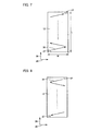
- FIGs. 7 and 8 show the deposition surface in substrate 12 (that surface which is opposed to target material 14).
- deposition region 27 in the surface of substrate 12 is a part of the entire surface of substrate 12.
- this deposition region 27 is gradually moved in the direction of arrow 30 as shown in Fig. 7, so that a prescribed film is formed continuously on the surface of substrate 12.
- Deposition region 27 moves from one end portion to the other end portion in the width W direction of substrate 12 as shown in Fig. 7, and at the same time, it gradually moves from one end portion toward the other end portion in the length L direction in the direction indicated by arrow 29.
- deposition region 27 in the surface of substrate 12 as shown in Fig. 7 can be realized in film deposition apparatus 1 shown in Fig. 1 in the following manner.
- plume 15 is formed by irradiating a prescribed region of target material 14 with laser light 16 with the position of target material 14 being kept constant.
- the position of plume 15 hardly moves, as the position of target material 14 and the optical axis of laser light 16 are fixed.
- XY stage 9 is operated to gradually move substrate 12 in the direction opposite to the direction of arrow 30.
- deposition region 27 can be moved in the surface of substrate 12.
- the speed at which substrate 12 is moved is determined in consideration of the deposition rate in deposition region 27, the size of deposition region 27, the size of substrate 12 (the width W and the length L), and the like.
- the moving speed and the moving direction of substrate 12 is determined so as not to cause a region where film is not formed in the surface of substrate 12 (in other words, the speed in the direction indicated by arrow 29 and the speed in the direction indicated by arrow 28 are balanced for the moving speed of substrate 12, so as not to cause a region that is not scanned by deposition region 27).
- deposition region 27 As shown in Fig. 7, after deposition region 27 reaches from the one end portion to the other end portion of substrate 12, substrate 12 is again moved in the direction opposite to that in the step shown in Fig. 7, as shown in Fig. 8. As a result, the deposition region can be moved from the other end portion to the one end portion in the length L direction in substrate 12. In this way, a film of a prescribed thickness can be formed by moving deposition region 27 in the surface of substrate 12.
- substrate 12 may be moved as shown in Fig. 9, in place of the method shown in Figs. 7 and 8.
- deposition region 27 is moved in the direction indicated by arrow 28, so that deposition region 27 is moved from the one end portion to the other end portion in the width direction of substrate 12.
- deposition region 27 is moved in the direction approximately parallel to arrow 29.
- Deposition region 27 is further moved in the direction opposite to the direction indicated by arrow 28, so that deposition region 27 is moved from the other end portion to the one end portion in the width direction of substrate 12.
- Deposition region 27 is then moved in the direction approximately parallel to arrow 29. The steps (a)-(d) above are repeated.
- deposition region 27 is moved in the direction approximately parallel to arrow 29 by a distance approximately equal in length to the width of deposition region 27 in the direction of arrow 29.
- a film can be formed densely and uniformly on the surface of substrate 12.
- the film deposition method using the film deposition apparatus shown in Figs. 1 and 2 can be applied to a deposition step for an oxide superconductor such as an RE123-based oxide superconductor or a bismuth-based oxide superconductor. In this case, it is possible to readily form a uniform oxide superconductor film on a large-area substrate.
- an oxide superconductor such as an RE123-based oxide superconductor or a bismuth-based oxide superconductor.
- the film deposition method using the film deposition apparatus in the present invention may be applied to a deposition step for an intermediate film arranged between a substrate and an oxide superconductor.
- the intermediate film formed by the deposition method in the present invention includes, for example, yttria-stabilized zirconia, cerium oxide, magnesium oxide, strontium titanate, or the like.
- substrate 12 on which an oxide superconductor film or an intermediate film is formed as described above sapphire, lanthanum aluminate, strontium titanate, or LSAT (Lanthanum Strontium Aluminum Titanium Oxide), or the like can be used.
- LSAT Long Strontium Aluminum Titanium Oxide
- the film deposition apparatus shown in Figs. 1 and 2 was used to prepare samples for measurement of film thicknesses, the number of particles, and the like, as described below.
- HoBa 2 Cu 3 O x superconductor film (referred to as HoBCO superconductor film hereinafter) was formed on a lanthanum aluminate substrate as a substrate using laser ablation.
- the lanthanum aluminate substrate used here is shaped like a rectangular having a width W of 3 cm and a length L of 10 cm.
- HoBCO sintered body of 20 centimeters square was used as a target material.
- the prepared samples include three kinds: a sample as a comparative example, and Samples 1 and 2 as examples.
- the deposition step for the sample as the comparative example employed the arrangement in which target material 14 and substrate 12 are approximately parallel to each other as shown in Fig. 3.
- the deposition step of Sample 1 as the example of the present invention employed the arrangement shown in Fig. 4 (specifically, the arrangement in which the direction of the optical axis of laser light 16 is approximately parallel to the direction of the surface of substrate 12).
- the deposition step of Sample 2 as an example employed the arrangement shown in Fig. 5 where target material 14 is perpendicular to substrate 12.
- XY stage 9 was operated to move deposition region 27 on substrate 12 using the method as shown in Figs. 7 and 8.
- the moving speed of substrate 12 was such that the speed in the direction parallel to arrow 29 shown in Fig. 7 and the speed in the direction parallel to arrow 28 were both 5 mm/sec.
- Substrate 12 was repeatedly scanned with deposition region 27, as shown in Figs. 7 and 8, thereby attaining a uniform thickness of HoBCO superconductor film formed on the surface of substrate 12.
- the same deposition conditions were basically used for these three kinds of sample, except the arrangement of the substrate.
- the temperature of substrate 12 in the deposition was 750°C.
- An oxygen gas atmosphere were introduced in chamber 2.
- the pressure within chamber 2 was set at 13.3Pa (100mTorr).
- the repetition frequency of laser light 16 was set at 20 Hz and the power of the laser light was set at 700 mJ.
- the incident angle ⁇ LT of laser light 16 with respect to the surface of target material 14 was set at 45°.
- the deposition time was 30 minutes for all of the samples.
- the thickest film was obtained in the sample of the comparative example where substrate 12 and target material 14 are arranged parallel to each other.
- the deposition time is consistently 30 minutes in any of the samples, the highest deposition rate was attained when substrate 12 and target material 14 are parallel to each other as in the comparative example, and the deposition rate is reduced with increasing inclination angle of the substrate with respect to the target material as Samples 1 and 2 of the examples.
- the number of particles in the formed film is greatest in the comparative example, and it is reduced in Samples 1 and 2 of the examples, accordingly. Therefore, it can be seen that it is effective to arrange the surface of substrate 12 approximately perpendicular to the surface of target material 14 as in Sample 2 of the example, in order to smooth significantly the surface of the formed film.
- substrate 12 does not interfere with the optical axis of laser light 16 even if substrate 12 is arbitrarily moved in the direction parallel to the surface thereof.
- the arrangement as in Sample 1 of the example allows substrate 12 to be increased in size without the constraints of the position of the optical axis of laser light.
- Samples 1 and 2 of the example have approximately equal critical current density Jc and exhibit a good property.
- the thickness of the formed superconductor film is reduced with increasing angle ⁇ between the substrate and the target (in other words, the deposition rate is lowered).
- the number of particles in the superconductor film is reduced.
- critical current density Jc exhibits a sufficient value.
- a sample as an example was prepared where HoBCO superconductor film was formed on substrate 12 using a rectangular-shaped lanthanum aluminate substrate having a width W of 5 cm and a length L of 20 cm as a substrate 12, with the angle ⁇ of 45° between target material 14 and substrate 12.
- substrate 12 was moved in the plane parallel to the surface of substrate 12. The moving speed of substrate 12 was such that both of the speed in the direction parallel to arrow 29 and the speed in the direction parallel to arrow 28 in Fig. 7 were 5 mm/sec.
- the other deposition conditions were basically similar to the deposition conditions for Sample 1 in Example 1.
- a sample was prepared as a comparative example where a deposition was performed using the following deposition conditions.
- the deposition conditions for the sample as the comparative example were similar to those in the aforementioned example in regard of the substrate temperature in deposition, the atmosphere gas and pressure, as well as the repetition frequency of laser and the laser power.
- a beam homogenizer of an optical system was used to expand irradiation region of laser light applied on the target material in order to form a deposition region larger than the width W in the shorter axial direction (the width W direction) of substrate 12.
- the energy variation of the beam homogenizer is ⁇ 5%, and a line beam having a width of 7 cm can be obtained.
- the size of plume 15 can be increased by irradiating the target material with the line beam with a width of 7 cm.
- the substrate is sized to have a width W of 5 cm and a length L of 20 cm. Therefore, the width of the deposition region on the substrate can be increased equivalently to the width W of the substrate. Accordingly, using the aforementioned beam homogenizer, a deposition region having a width equivalent to the width W of the substrate (5 cm) was formed on substrate 12 in the comparative example. Substrate 12 was transferred only in the length L direction (only in a single-dimensional direction) with the arrangement of the deposition region extending from the one end portion to the other end portion in the width W direction of the substrate. In this way, in the sample as the comparative example, an oxide superconductor film was formed over the entire substrate.
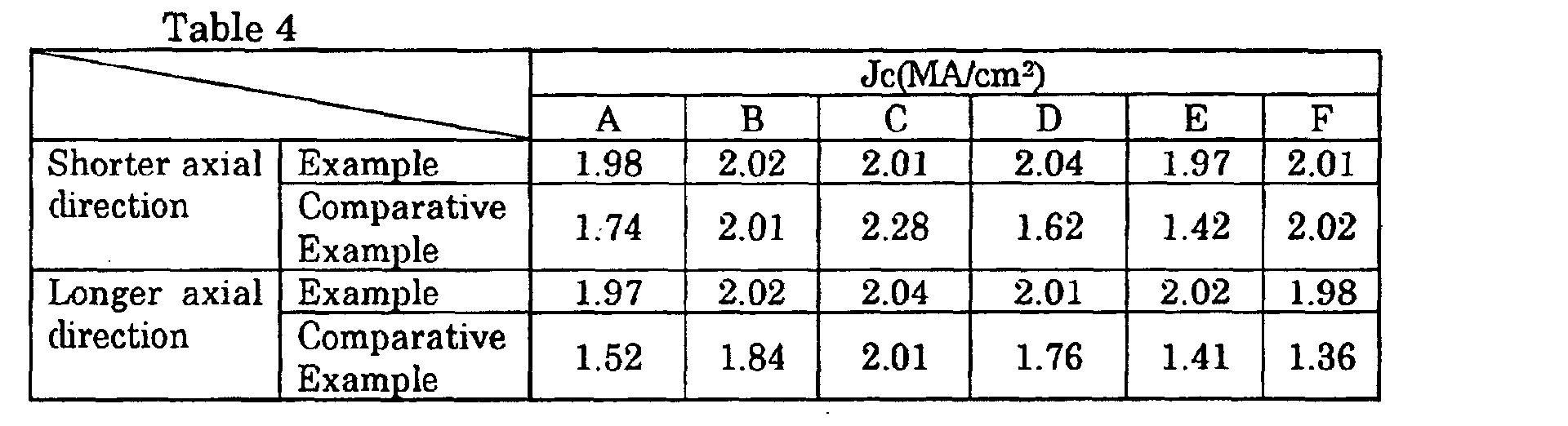
- the shorter axial direction refers to the width W direction shown in Figs. 7 and 8
- the longer axial direction refers to the length L direction shown in Figs 7 and 8.
- the thicknesses of the oxide superconductor film were measured at six points A-F arranged at regular intervals in each of these directions. As a result, as can be seen from Table 3, the sample of the example has a film thickness variation smaller than the comparative example.
- the example of the present invention has a critical current density Jc variation smaller than the comparative example.
- samples as the example and the comparative example were prepared where a cerium oxide intermediate layer was deposited on the sapphire substrate using laser ablation.
- the deposition step for the cerium oxide intermediate layer in the sample of the example employed the arrangement of target material 14, substrate 12 and laser light 16 which was similar to the arrangement in the deposition step for the sample as the example in Example 3.
- the substrate temperature in deposition was 600°C
- the atmosphere was argon gas
- the pressure of the atmosphere was 13.3 Pa (100mTorr)
- the repetition frequency of laser was 150 Hz
- the laser power was 600 mJ.
- substrate 12 was moved as shown in Figs. 7 and 8 in the manner similar to the sample as the example in Example 3.
- the conditions such as the moving speed at which substrate 12 is moved is similar to the conditions such as the moving speed of the substrate in the sample of the example in Example 3.
- a beam homogenizer was used in a manner similar to the comparative example in Example 3.
- the other deposition conditions were similar to the deposition conditions in the example in Example 4 described above.
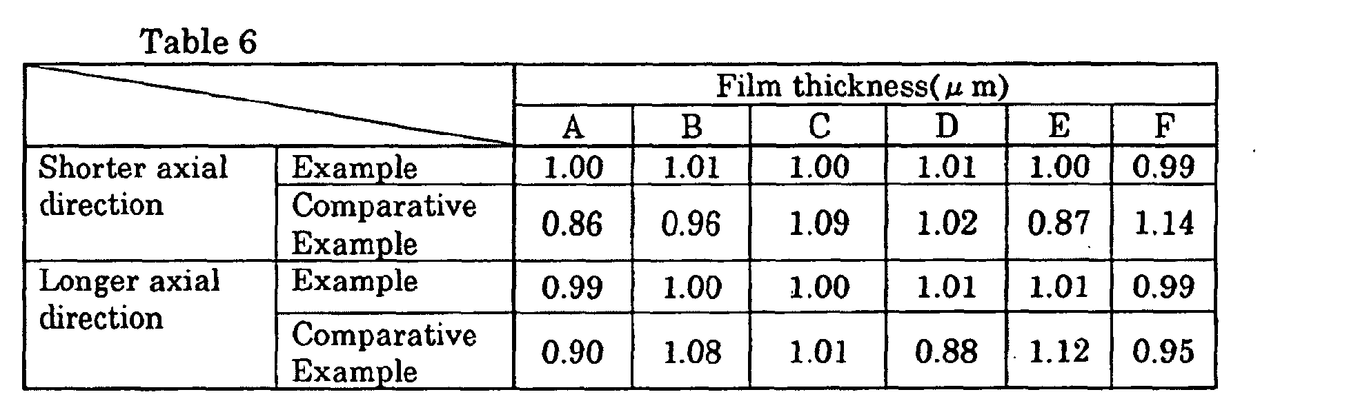
- the measurement was performed at six points of A-F arranged at regular intervals in both of the shorter axial direction and the longer axial direction, similarly to Example 3.
- the example has a film thickness variation in the cerium oxide intermediate layer smaller than the comparative example.
- the sample of the example in Example 5 was prepared by forming HoBCO superconductor film on the cerium oxide intermediate layer in the sample of the example in Example 4, under the deposition conditions similar to those in the sample of the example in Example 3.
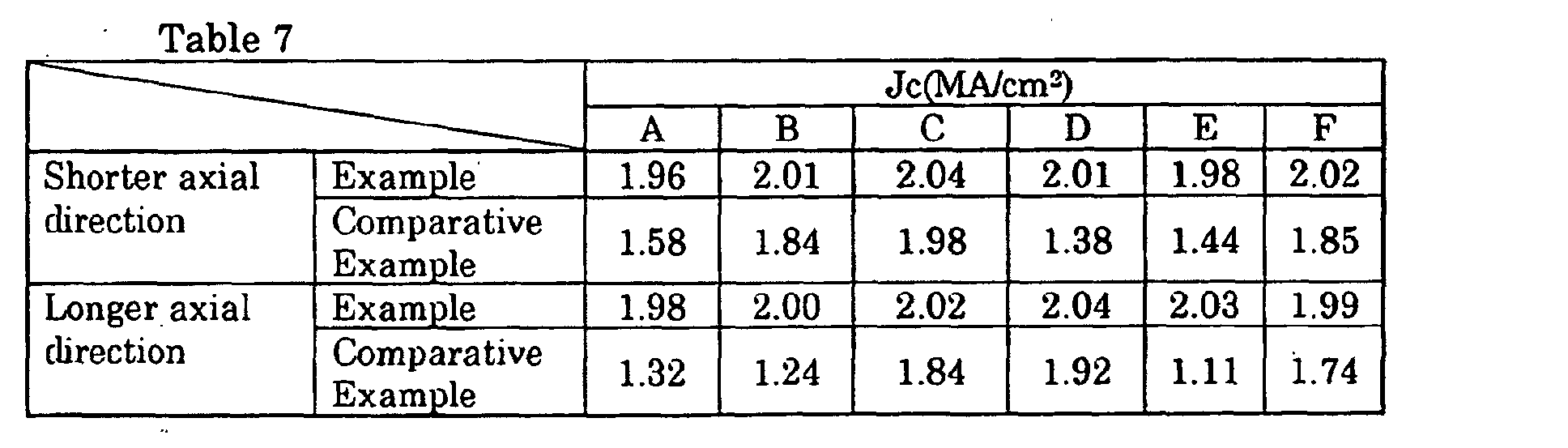
- HoBCO superconductor film was formed on the cerium oxide intermediate layer in the sample of the comparative example in Example 4, under the deposition conditions similar to those in the comparative example in Example 3 (that is, the conditions using a beam homogenizer).
- the film thickness and critical current density Jc were measured at the measurement points A-F arranged at regular intervals in each of the shorter axial direction and the longer axial direction, similarly to Examples 3 and 4.
- the example has a film thickness variation smaller than the comparative example and also has a smaller critical current density Jc variation.
- the film deposition method and apparatus in accordance with the present invention can be used as a method and apparatus for forming a film on a surface of a large-area substrate.
Landscapes
- Chemical & Material Sciences (AREA)
- Engineering & Computer Science (AREA)
- Chemical Kinetics & Catalysis (AREA)
- Materials Engineering (AREA)
- Mechanical Engineering (AREA)
- Metallurgy (AREA)
- Organic Chemistry (AREA)
- Toxicology (AREA)
- Health & Medical Sciences (AREA)
- Manufacturing & Machinery (AREA)
- Physical Vapour Deposition (AREA)
- Superconductors And Manufacturing Methods Therefor (AREA)
- Magnetic Heads (AREA)
- Preparing Plates And Mask In Photomechanical Process (AREA)
- Internal Circuitry In Semiconductor Integrated Circuit Devices (AREA)
- Manufacturing Of Electric Cables (AREA)
- Extrusion Moulding Of Plastics Or The Like (AREA)
- Physical Deposition Of Substances That Are Components Of Semiconductor Devices (AREA)
- Superconductor Devices And Manufacturing Methods Thereof (AREA)
Abstract
Description
| Film thickness (µm) | Number of particles (Number /100 µm2) | Jc (MA/cm2) | Others | ||
| Comparative Example | 6.25 | 107 | 3.12 | Substrate-target : parallel | |
| Example | Sample 1 | 4.01 | 53 | 3.15 | Substrate-laser light : |
| Sample | |||||
| 2 | 1.13 | 3 | 3.08 | Substrate-target: perpendicular |
| ID | Angle between substrate and target :(°) | Film thickness (µm) | Number of particles (Number/100µm2) | Jc (MA/cm2) |
| Sample 1 | 45 | 4.01 | 53 | 3.15 |
| | 60 | 3.16 | 37 | 3.14 |
| | 75 | 2.51 | 21 | 3.13 |
| | 90 | 1.13 | 3 | 3.08 |


Claims (17)
- A film deposition method of forming a film by scattering a deposition material from a surface of a target material (14) and depositing the scattered deposition material onto a surface of a substrate (12), comprising:a step of arranging said substrate (12) and said target material (14) such that the surface of said substrate (12) forms an angle to the surface of the target material (14); anda deposition step of forming said film on said substrate (12) in such a manner that an area of a surface of said film is continuously increased in a two-dimensional direction, while moving a relative position of said substrate (12) with respect to said target material (14).
- The film deposition method according to claim 1, wherein an angle () between the surface of said substrate (12) and the surface of said target material (14) exceeds 0° and is equal to or less than 90°.
- The film deposition method according to claim 1, wherein energy rays (16) are applied to the surface of said target material (14) in order to scatter the deposition material from the surface of said target material (14).
- The film deposition method according to claim 3, wherein an angle (LT) between a path (25) of said energy rays (16) and the surface of said target material (14) is smaller than an angle () between the surface of said substrate (12) and the surface of said target material (14).
- The film deposition method according to claim 3, wherein a path (25) of said energy rays (16) is approximately parallel to the surface of said substrate (12).
- The film deposition method according to claim 1, further comprising an angle varying step of changing an angle () between the surface of said substrate (12) and the surface of said target material (14) by varying a relative position of said substrate (12) with respect to said target material (14).
- The film deposition method according to claim 1, wherein, in said deposition step, a moving direction in which a relative position of said substrate (12) with respect to said target material (14) is moved is approximately parallel to the surface of said substrate (12).
- The film deposition method according to claim 1, wherein said film includes an oxide superconductor.
- The film deposition method according to claim 8, wherein said oxide superconductor includes one kind selected from the group consisting of an RE123-based oxide superconductor and a bismuth-based oxide superconductor.
- The film deposition method according to claim 1, further comprising a step of forming an oxide superconductor on said film, wherein
said film is an intermediate film positioned between said substrate (12) and said oxide superconductor. - The film deposition method according to claim 10, wherein said film includes at least one kind selected from the group consisting of yttria-stabilized zirconia, cerium oxide, magnesium oxide, and strontium titanate.
- The film deposition method according to claim 1, wherein a material forming said substrate (12) includes at least one selected from the group consisting of sapphire, lanthanum aluminate, strontium titanate, and LSAT.
- A film deposition apparatus (1) to form a thin film by scattering a deposition material from a surface of a target material (14) and depositing the scattered deposition material onto a surface of a substrate (12), comprising
varying means (4-6, 9-11, 21) for varying an angle of the surface of said substrate (12) to the surface of the target material (14). - The film deposition apparatus according to claim 13, wherein said varying means (4-6, 9-11, 21) includes
an arc-shaped guide member (4), and
a substrate holding member (11) movably mounted to said guide member (4) for holding said substrate (12). - The film deposition apparatus according to claim 13 further comprising moving means (9) for moving a relative position of said substrate (12) with respect to said target material (14).
- The film deposition apparatus according to claim 15, wherein said moving means (9) moves the relative position of said substrate (12) with respect to said target material (14) in the direction approximately parallel to the surface of said substrate (12).
- The film deposition apparatus according to claim 13 further comprising irradiation means for irradiating the surface of said target material (14) with energy rays (16) in order to scatter the deposition material from the surface of said target material (14).
Applications Claiming Priority (3)
| Application Number | Priority Date | Filing Date | Title |
|---|---|---|---|
| JP2001032280A JP2002235168A (en) | 2001-02-08 | 2001-02-08 | Film forming method and film forming apparatus |
| JP2001032280 | 2001-02-08 | ||
| PCT/JP2002/000936 WO2002063063A1 (en) | 2001-02-08 | 2002-02-05 | Film forming method and film forming device |
Publications (3)
| Publication Number | Publication Date |
|---|---|
| EP1371746A1 true EP1371746A1 (en) | 2003-12-17 |
| EP1371746A4 EP1371746A4 (en) | 2004-06-16 |
| EP1371746B1 EP1371746B1 (en) | 2006-03-22 |
Family
ID=18896239
Family Applications (1)
| Application Number | Title | Priority Date | Filing Date |
|---|---|---|---|
| EP02710513A Expired - Lifetime EP1371746B1 (en) | 2001-02-08 | 2002-02-05 | Film forming method and film forming device |
Country Status (13)
| Country | Link |
|---|---|
| US (1) | US20040096580A1 (en) |
| EP (1) | EP1371746B1 (en) |
| JP (1) | JP2002235168A (en) |
| KR (1) | KR100819719B1 (en) |
| CN (1) | CN1265016C (en) |
| AT (1) | ATE321154T1 (en) |
| AU (1) | AU2002228436B2 (en) |
| CA (1) | CA2436750C (en) |
| DE (1) | DE60210045T2 (en) |
| DK (1) | DK1371746T3 (en) |
| ES (1) | ES2261642T3 (en) |
| NZ (1) | NZ527521A (en) |
| WO (1) | WO2002063063A1 (en) |
Cited By (2)
| Publication number | Priority date | Publication date | Assignee | Title |
|---|---|---|---|---|
| DE102006028977B4 (en) * | 2006-06-23 | 2012-04-12 | Qimonda Ag | Sputterdepositions device |
| US12243715B2 (en) | 2017-12-22 | 2025-03-04 | Institute Of Geological And Nuclear Sciences Limited | Ion beam sputtering apparatus and method |
Families Citing this family (7)
| Publication number | Priority date | Publication date | Assignee | Title |
|---|---|---|---|---|
| JP5244725B2 (en) * | 2009-07-21 | 2013-07-24 | 株式会社日立ハイテクノロジーズ | Deposition equipment |
| MY174290A (en) * | 2012-02-03 | 2020-04-02 | Seagate Technology Llc | Methods of forming layers |
| CN106544634B (en) * | 2015-09-17 | 2019-03-12 | 宁波江丰电子材料股份有限公司 | A kind of forming method of film layer, target and target production method |
| CN107630188A (en) * | 2017-10-31 | 2018-01-26 | 安徽富芯微电子有限公司 | A kind of film-coating mechanism and its application method for being used to improve metal level plating film uniformity |
| CN108165934B (en) * | 2018-01-19 | 2020-06-16 | 武汉华美晨曦光电有限责任公司 | Evaporation plating equipment |
| CN114250164B (en) * | 2020-09-23 | 2023-11-17 | 中国农业大学 | A kind of Acinetobacter 1502IPR-05 with nitrogen-fixing and phosphorus-solubilizing ability and its application |
| US20240318301A1 (en) * | 2021-07-28 | 2024-09-26 | MAX-PLANCK-Gesellschaft zur Förderung der Wissenschaften e.V. | Apparatus for a thermal evaporation system and method of coating a coating region on a front surface of a substrate |
Family Cites Families (18)
| Publication number | Priority date | Publication date | Assignee | Title |
|---|---|---|---|---|
| JPS5736437A (en) * | 1980-08-14 | 1982-02-27 | Fuji Photo Film Co Ltd | Producing device of magnetic recording medium |
| JPS6194242A (en) * | 1984-10-16 | 1986-05-13 | Fuji Photo Film Co Ltd | Manufacture of magnetic recording medium |
| JPH0533124A (en) * | 1991-07-26 | 1993-02-09 | Olympus Optical Co Ltd | Laser flash deposition equipment |
| US5332133A (en) * | 1991-11-01 | 1994-07-26 | Nisshin Flour Milling Co., Ltd. | Powder supplying apparatus and powder spraying apparatus |
| JPH06101037A (en) * | 1992-09-22 | 1994-04-12 | Hitachi Ltd | Ion beam sputtering system |
| US5650378A (en) * | 1992-10-02 | 1997-07-22 | Fujikura Ltd. | Method of making polycrystalline thin film and superconducting oxide body |
| JP2996568B2 (en) * | 1992-10-30 | 2000-01-11 | 株式会社フジクラ | Method for producing polycrystalline thin film and method for producing oxide superconducting conductor |
| WO1994020295A1 (en) * | 1993-03-12 | 1994-09-15 | Neocera, Inc. | Superconducting films on alkaline earth fluoride substrates with multiple buffer layers |
| JPH06271394A (en) * | 1993-03-19 | 1994-09-27 | Chodendo Hatsuden Kanren Kiki Zairyo Gijutsu Kenkyu Kumiai | Target for laser deposition apparatus and method for manufacturing oxide superconductor using the same |
| US5411772A (en) * | 1994-01-25 | 1995-05-02 | Rockwell International Corporation | Method of laser ablation for uniform thin film deposition |
| JPH0870144A (en) * | 1994-08-26 | 1996-03-12 | Sumitomo Electric Ind Ltd | How to make superconducting parts |
| JPH08144051A (en) * | 1994-11-21 | 1996-06-04 | Matsushita Electric Ind Co Ltd | Thin film forming method using laser ablation and laser ablation apparatus |
| US5624722A (en) * | 1995-03-07 | 1997-04-29 | Sumitomo Electric Industries, Ltd. | Apparatus and method for depositing films on substrate via on-axis laser ablation |
| JPH08246134A (en) * | 1995-03-07 | 1996-09-24 | Sumitomo Electric Ind Ltd | Thin film manufacturing method and thin film manufacturing apparatus by laser deposition method |
| JP3771012B2 (en) * | 1997-09-02 | 2006-04-26 | 株式会社フジクラ | Oxide superconducting conductor |
| US6090207A (en) * | 1998-04-02 | 2000-07-18 | Neocera, Inc. | Translational target assembly for thin film deposition system |
| JP3877903B2 (en) * | 1999-04-28 | 2007-02-07 | 株式会社フジクラ | Thin film formation method |
| JP2002266072A (en) * | 2001-03-09 | 2002-09-18 | Sumitomo Electric Ind Ltd | Laminated film and film forming method |
-
2001
- 2001-02-08 JP JP2001032280A patent/JP2002235168A/en not_active Withdrawn
-
2002
- 2002-02-05 AT AT02710513T patent/ATE321154T1/en not_active IP Right Cessation
- 2002-02-05 DE DE60210045T patent/DE60210045T2/en not_active Expired - Lifetime
- 2002-02-05 NZ NZ527521A patent/NZ527521A/en unknown
- 2002-02-05 KR KR1020037010471A patent/KR100819719B1/en not_active Expired - Fee Related
- 2002-02-05 CA CA002436750A patent/CA2436750C/en not_active Expired - Fee Related
- 2002-02-05 DK DK02710513T patent/DK1371746T3/en active
- 2002-02-05 CN CNB028044746A patent/CN1265016C/en not_active Expired - Fee Related
- 2002-02-05 EP EP02710513A patent/EP1371746B1/en not_active Expired - Lifetime
- 2002-02-05 US US10/466,330 patent/US20040096580A1/en not_active Abandoned
- 2002-02-05 WO PCT/JP2002/000936 patent/WO2002063063A1/en not_active Ceased
- 2002-02-05 ES ES02710513T patent/ES2261642T3/en not_active Expired - Lifetime
- 2002-02-05 AU AU2002228436A patent/AU2002228436B2/en not_active Ceased
Cited By (2)
| Publication number | Priority date | Publication date | Assignee | Title |
|---|---|---|---|---|
| DE102006028977B4 (en) * | 2006-06-23 | 2012-04-12 | Qimonda Ag | Sputterdepositions device |
| US12243715B2 (en) | 2017-12-22 | 2025-03-04 | Institute Of Geological And Nuclear Sciences Limited | Ion beam sputtering apparatus and method |
Also Published As
| Publication number | Publication date |
|---|---|
| NZ527521A (en) | 2006-04-28 |
| WO2002063063A1 (en) | 2002-08-15 |
| DE60210045D1 (en) | 2006-05-11 |
| EP1371746A4 (en) | 2004-06-16 |
| AU2002228436B2 (en) | 2007-05-24 |
| CN1265016C (en) | 2006-07-19 |
| DK1371746T3 (en) | 2006-07-31 |
| CN1489638A (en) | 2004-04-14 |
| JP2002235168A (en) | 2002-08-23 |
| DE60210045T2 (en) | 2007-03-29 |
| EP1371746B1 (en) | 2006-03-22 |
| US20040096580A1 (en) | 2004-05-20 |
| CA2436750A1 (en) | 2002-08-15 |
| KR100819719B1 (en) | 2008-04-07 |
| CA2436750C (en) | 2008-12-30 |
| ATE321154T1 (en) | 2006-04-15 |
| ES2261642T3 (en) | 2006-11-16 |
| KR20030076664A (en) | 2003-09-26 |
Similar Documents
| Publication | Publication Date | Title |
|---|---|---|
| JP2660248B2 (en) | Film formation method using light | |
| Christen et al. | Recent advances in pulsed-laser deposition of complex oxides | |
| US5952271A (en) | Method for manufacturing oxide superconducting films via laser ablation followed by laser material processing | |
| EP0581254B1 (en) | Method of forming single-crystalline thin film | |
| CA2436750C (en) | Film deposition method and film deposition apparatus | |
| EP0702416B1 (en) | Method and apparatus for depositing superconducting layer onto the substrate surface via off-axis laser ablation | |
| DE69132079T2 (en) | Device for forming a thin layer of oxide superconductor | |
| JP2007525790A (en) | Superconductor method and reactor | |
| Iembo et al. | In situ diagnostics of pulsed laser deposition of ferroelectric Pb (Ti0. 48Zr0. 52) O3 on Si | |
| US20120015814A1 (en) | HTS coated conductor with particle inclusions, and method of production of an HTS coated conductor | |
| CA2016354C (en) | Method of fabricating oxide superconducting film | |
| KR100764527B1 (en) | Lamination Film and Film Formation Method | |
| Guan et al. | Synthesis of aligned nanoparticles on laser-generated templates | |
| Dam et al. | The laser ablation threshold of YBa2Cu3O6+ x as revealed by using projection optics | |
| JP2023076209A (en) | Multifilamentary thin-film superconducting wire and its manufacturing method | |
| JPH0885865A (en) | Method of forming thin film by laser deposition method | |
| JP2810930B2 (en) | Film forming method using laser light | |
| Wu et al. | The relationship between microstructure and residual stress in YBa2Cu3O7− x | |
| EP0526331B1 (en) | Method for preparing a superconducting thin film of compound oxide | |
| JP6155402B2 (en) | Superconducting wire and method for manufacturing the same | |
| JPH07216539A (en) | Film forming apparatus and thin film manufacturing method using the same | |
| JP2003317557A (en) | Wire rod manufacturing method and wire rod manufacturing apparatus | |
| McIntyre | Heteroepitaxial growth of chemically derived Ba₂YCu₃O₇â x thin films | |
| Karmanenko et al. | Sources of flicker noise and the technology of superconducting microstripes based on yttrium barium cuprate films | |
| JPH0741946A (en) | Laser vapor deposition apparatus and method for forming polycrystalline thin film using the same |
Legal Events
| Date | Code | Title | Description |
|---|---|---|---|
| PUAI | Public reference made under article 153(3) epc to a published international application that has entered the european phase |
Free format text: ORIGINAL CODE: 0009012 |
|
| 17P | Request for examination filed |
Effective date: 20030813 |
|
| AK | Designated contracting states |
Kind code of ref document: A1 Designated state(s): AT BE CH CY DE DK ES FI FR GB GR IE IT LI LU MC NL PT SE TR |
|
| RIN1 | Information on inventor provided before grant (corrected) |
Inventor name: OHMATSU,KC/O OSAKA WORKS OF SUMITOMO ELECT IND LTD Inventor name: HAHAKURA,SC/O OSAKA WORKS OFSUMITOMO ELECT IND LTD |
|
| A4 | Supplementary search report drawn up and despatched |
Effective date: 20040506 |
|
| RIC1 | Information provided on ipc code assigned before grant |
Ipc: 7C 23C 14/56 B Ipc: 7C 23C 14/50 B Ipc: 7C 23C 14/28 A |
|
| 17Q | First examination report despatched |
Effective date: 20040716 |
|
| GRAP | Despatch of communication of intention to grant a patent |
Free format text: ORIGINAL CODE: EPIDOSNIGR1 |
|
| GRAS | Grant fee paid |
Free format text: ORIGINAL CODE: EPIDOSNIGR3 |
|
| GRAA | (expected) grant |
Free format text: ORIGINAL CODE: 0009210 |
|
| AK | Designated contracting states |
Kind code of ref document: B1 Designated state(s): AT BE CH CY DE DK ES FI FR GB GR IE IT LI LU MC NL PT SE TR |
|
| PG25 | Lapsed in a contracting state [announced via postgrant information from national office to epo] |
Ref country code: AT Free format text: LAPSE BECAUSE OF FAILURE TO SUBMIT A TRANSLATION OF THE DESCRIPTION OR TO PAY THE FEE WITHIN THE PRESCRIBED TIME-LIMIT Effective date: 20060322 Ref country code: IT Free format text: LAPSE BECAUSE OF FAILURE TO SUBMIT A TRANSLATION OF THE DESCRIPTION OR TO PAY THE FEE WITHIN THE PRESCRIBED TIME-LIMIT;WARNING: LAPSES OF ITALIAN PATENTS WITH EFFECTIVE DATE BEFORE 2007 MAY HAVE OCCURRED AT ANY TIME BEFORE 2007. THE CORRECT EFFECTIVE DATE MAY BE DIFFERENT FROM THE ONE RECORDED. Effective date: 20060322 |
|
| REG | Reference to a national code |
Ref country code: GB Ref legal event code: FG4D |
|
| REG | Reference to a national code |
Ref country code: CH Ref legal event code: EP |
|
| REG | Reference to a national code |
Ref country code: IE Ref legal event code: FG4D |
|
| REF | Corresponds to: |
Ref document number: 60210045 Country of ref document: DE Date of ref document: 20060511 Kind code of ref document: P |
|
| PG25 | Lapsed in a contracting state [announced via postgrant information from national office to epo] |
Ref country code: SE Free format text: LAPSE BECAUSE OF FAILURE TO SUBMIT A TRANSLATION OF THE DESCRIPTION OR TO PAY THE FEE WITHIN THE PRESCRIBED TIME-LIMIT Effective date: 20060622 |
|
| REG | Reference to a national code |
Ref country code: DK Ref legal event code: T3 Ref country code: CH Ref legal event code: NV Representative=s name: ROSENICH PAUL; GISLER CHRISTIAN PATENTBUERO PAUL R |
|
| PG25 | Lapsed in a contracting state [announced via postgrant information from national office to epo] |
Ref country code: PT Free format text: LAPSE BECAUSE OF FAILURE TO SUBMIT A TRANSLATION OF THE DESCRIPTION OR TO PAY THE FEE WITHIN THE PRESCRIBED TIME-LIMIT Effective date: 20060822 |
|
| REG | Reference to a national code |
Ref country code: ES Ref legal event code: FG2A Ref document number: 2261642 Country of ref document: ES Kind code of ref document: T3 |
|
| ET | Fr: translation filed | ||
| PLBE | No opposition filed within time limit |
Free format text: ORIGINAL CODE: 0009261 |
|
| STAA | Information on the status of an ep patent application or granted ep patent |
Free format text: STATUS: NO OPPOSITION FILED WITHIN TIME LIMIT |
|
| 26N | No opposition filed |
Effective date: 20061227 |
|
| PG25 | Lapsed in a contracting state [announced via postgrant information from national office to epo] |
Ref country code: MC Free format text: LAPSE BECAUSE OF NON-PAYMENT OF DUE FEES Effective date: 20070228 |
|
| PG25 | Lapsed in a contracting state [announced via postgrant information from national office to epo] |
Ref country code: IE Free format text: LAPSE BECAUSE OF NON-PAYMENT OF DUE FEES Effective date: 20070205 |
|
| PG25 | Lapsed in a contracting state [announced via postgrant information from national office to epo] |
Ref country code: GR Free format text: LAPSE BECAUSE OF FAILURE TO SUBMIT A TRANSLATION OF THE DESCRIPTION OR TO PAY THE FEE WITHIN THE PRESCRIBED TIME-LIMIT Effective date: 20060623 |
|
| PG25 | Lapsed in a contracting state [announced via postgrant information from national office to epo] |
Ref country code: FI Free format text: LAPSE BECAUSE OF FAILURE TO SUBMIT A TRANSLATION OF THE DESCRIPTION OR TO PAY THE FEE WITHIN THE PRESCRIBED TIME-LIMIT Effective date: 20060322 |
|
| PG25 | Lapsed in a contracting state [announced via postgrant information from national office to epo] |
Ref country code: CY Free format text: LAPSE BECAUSE OF FAILURE TO SUBMIT A TRANSLATION OF THE DESCRIPTION OR TO PAY THE FEE WITHIN THE PRESCRIBED TIME-LIMIT Effective date: 20060322 Ref country code: LU Free format text: LAPSE BECAUSE OF NON-PAYMENT OF DUE FEES Effective date: 20070205 |
|
| PG25 | Lapsed in a contracting state [announced via postgrant information from national office to epo] |
Ref country code: TR Free format text: LAPSE BECAUSE OF FAILURE TO SUBMIT A TRANSLATION OF THE DESCRIPTION OR TO PAY THE FEE WITHIN THE PRESCRIBED TIME-LIMIT Effective date: 20060322 |
|
| PGFP | Annual fee paid to national office [announced via postgrant information from national office to epo] |
Ref country code: DK Payment date: 20110210 Year of fee payment: 10 |
|
| PGFP | Annual fee paid to national office [announced via postgrant information from national office to epo] |
Ref country code: FR Payment date: 20110218 Year of fee payment: 10 Ref country code: DE Payment date: 20110208 Year of fee payment: 10 Ref country code: NL Payment date: 20110304 Year of fee payment: 10 Ref country code: IT Payment date: 20110212 Year of fee payment: 10 Ref country code: CH Payment date: 20110214 Year of fee payment: 10 |
|
| PGFP | Annual fee paid to national office [announced via postgrant information from national office to epo] |
Ref country code: ES Payment date: 20110218 Year of fee payment: 10 Ref country code: GB Payment date: 20110209 Year of fee payment: 10 Ref country code: BE Payment date: 20110211 Year of fee payment: 10 |
|
| BERE | Be: lapsed |
Owner name: *SUMITOMO ELECTRIC INDUSTRIES LTD Effective date: 20120228 |
|
| REG | Reference to a national code |
Ref country code: NL Ref legal event code: V1 Effective date: 20120901 |
|
| REG | Reference to a national code |
Ref country code: CH Ref legal event code: PL |
|
| GBPC | Gb: european patent ceased through non-payment of renewal fee |
Effective date: 20120205 |
|
| PG25 | Lapsed in a contracting state [announced via postgrant information from national office to epo] |
Ref country code: LI Free format text: LAPSE BECAUSE OF NON-PAYMENT OF DUE FEES Effective date: 20120229 Ref country code: CH Free format text: LAPSE BECAUSE OF NON-PAYMENT OF DUE FEES Effective date: 20120229 |
|
| REG | Reference to a national code |
Ref country code: DK Ref legal event code: EBP |
|
| REG | Reference to a national code |
Ref country code: FR Ref legal event code: ST Effective date: 20121031 |
|
| PG25 | Lapsed in a contracting state [announced via postgrant information from national office to epo] |
Ref country code: IT Free format text: LAPSE BECAUSE OF NON-PAYMENT OF DUE FEES Effective date: 20120205 |
|
| REG | Reference to a national code |
Ref country code: DE Ref legal event code: R119 Ref document number: 60210045 Country of ref document: DE Effective date: 20120901 |
|
| PG25 | Lapsed in a contracting state [announced via postgrant information from national office to epo] |
Ref country code: BE Free format text: LAPSE BECAUSE OF NON-PAYMENT OF DUE FEES Effective date: 20120228 |
|
| PG25 | Lapsed in a contracting state [announced via postgrant information from national office to epo] |
Ref country code: NL Free format text: LAPSE BECAUSE OF NON-PAYMENT OF DUE FEES Effective date: 20120901 Ref country code: FR Free format text: LAPSE BECAUSE OF NON-PAYMENT OF DUE FEES Effective date: 20120229 Ref country code: GB Free format text: LAPSE BECAUSE OF NON-PAYMENT OF DUE FEES Effective date: 20120205 |
|
| PG25 | Lapsed in a contracting state [announced via postgrant information from national office to epo] |
Ref country code: DE Free format text: LAPSE BECAUSE OF NON-PAYMENT OF DUE FEES Effective date: 20120901 |
|
| REG | Reference to a national code |
Ref country code: ES Ref legal event code: FD2A Effective date: 20130708 |
|
| PG25 | Lapsed in a contracting state [announced via postgrant information from national office to epo] |
Ref country code: ES Free format text: LAPSE BECAUSE OF NON-PAYMENT OF DUE FEES Effective date: 20120206 |
|
| PG25 | Lapsed in a contracting state [announced via postgrant information from national office to epo] |
Ref country code: DK Free format text: LAPSE BECAUSE OF NON-PAYMENT OF DUE FEES Effective date: 20120229 |