EP1369909A1 - Procédé de fabrication d'un transistor MOS de longueur de grille réduite, et ciruit intégré comportant un tel transistor - Google Patents
Procédé de fabrication d'un transistor MOS de longueur de grille réduite, et ciruit intégré comportant un tel transistor Download PDFInfo
- Publication number
- EP1369909A1 EP1369909A1 EP03291262A EP03291262A EP1369909A1 EP 1369909 A1 EP1369909 A1 EP 1369909A1 EP 03291262 A EP03291262 A EP 03291262A EP 03291262 A EP03291262 A EP 03291262A EP 1369909 A1 EP1369909 A1 EP 1369909A1
- Authority
- EP
- European Patent Office
- Prior art keywords
- intermediate layer
- transistor
- substrate
- implantation
- gate
- Prior art date
- Legal status (The legal status is an assumption and is not a legal conclusion. Google has not performed a legal analysis and makes no representation as to the accuracy of the status listed.)
- Granted
Links
Images

Classifications
-
- H—ELECTRICITY
- H10—SEMICONDUCTOR DEVICES; ELECTRIC SOLID-STATE DEVICES NOT OTHERWISE PROVIDED FOR
- H10P—GENERIC PROCESSES OR APPARATUS FOR THE MANUFACTURE OR TREATMENT OF DEVICES COVERED BY CLASS H10
- H10P30/00—Ion implantation into wafers, substrates or parts of devices
- H10P30/20—Ion implantation into wafers, substrates or parts of devices into semiconductor materials, e.g. for doping
- H10P30/202—Ion implantation into wafers, substrates or parts of devices into semiconductor materials, e.g. for doping characterised by the semiconductor materials
- H10P30/204—Ion implantation into wafers, substrates or parts of devices into semiconductor materials, e.g. for doping characterised by the semiconductor materials into Group IV semiconductors
-
- H—ELECTRICITY
- H10—SEMICONDUCTOR DEVICES; ELECTRIC SOLID-STATE DEVICES NOT OTHERWISE PROVIDED FOR
- H10D—INORGANIC ELECTRIC SEMICONDUCTOR DEVICES
- H10D30/00—Field-effect transistors [FET]
- H10D30/01—Manufacture or treatment
- H10D30/021—Manufacture or treatment of FETs having insulated gates [IGFET]
- H10D30/0223—Manufacture or treatment of FETs having insulated gates [IGFET] having source and drain regions or source and drain extensions self-aligned to sides of the gate
- H10D30/0227—Manufacture or treatment of FETs having insulated gates [IGFET] having source and drain regions or source and drain extensions self-aligned to sides of the gate having both lightly-doped source and drain extensions and source and drain regions self-aligned to the sides of the gate, e.g. lightly-doped drain [LDD] MOSFET or double-diffused drain [DDD] MOSFET
-
- H—ELECTRICITY
- H10—SEMICONDUCTOR DEVICES; ELECTRIC SOLID-STATE DEVICES NOT OTHERWISE PROVIDED FOR
- H10D—INORGANIC ELECTRIC SEMICONDUCTOR DEVICES
- H10D64/00—Electrodes of devices having potential barriers
- H10D64/01—Manufacture or treatment
- H10D64/021—Manufacture or treatment using multiple gate spacer layers, e.g. bilayered sidewall spacers
-
- H—ELECTRICITY
- H10—SEMICONDUCTOR DEVICES; ELECTRIC SOLID-STATE DEVICES NOT OTHERWISE PROVIDED FOR
- H10P—GENERIC PROCESSES OR APPARATUS FOR THE MANUFACTURE OR TREATMENT OF DEVICES COVERED BY CLASS H10
- H10P30/00—Ion implantation into wafers, substrates or parts of devices
- H10P30/20—Ion implantation into wafers, substrates or parts of devices into semiconductor materials, e.g. for doping
- H10P30/21—Ion implantation into wafers, substrates or parts of devices into semiconductor materials, e.g. for doping of electrically active species
- H10P30/212—Through-implantation
Definitions
- the invention relates to integrated circuits, and in particular not exclusively isolated gate field effect transistors (MOSFET transistors) of reduced gate length, for example less than 180 nanometers, and in particular those of nanometric, that is to say, whose gate length is less than About 100 nm.
- MOSFET transistors isolated gate field effect transistors
- MOS transistors of reduced dimensions in particular nanoscale, and classical architecture, collides today to intrinsic problems limiting their operating characteristics.
- short channels lowering the threshold voltage of the transistor when the length of grid decreases and therefore the channel length decreases
- reducing the depth of the junctions of these areas is accompanied by an increase in the resistance of these junctions when the depths become less than 40 nm in the case of the usual manufacturing processes which provide for a ion implantation of the dopant species (typically boron and arsenic), followed by thermal activation by high-temperature annealing temperature.
- the dopant species typically boron and arsenic
- the increase of the layer resistance of the junction increases the value of parasitic resistance of the device, limiting and the saturation current performance of the transistors.
- technological difficulties may include making a conformal deposition of a silicon-based material, the anisotropic and selective etching of this deposit with stop on the zone active, whatever the surface density of the transistors, as well as the realization of standard spacers which must be readjusted.
- offset spacers are usually manufactured with silicon based materials and it is therefore necessary to make an anisotropic etching of the compliant deposits in order to reduce the thickness of deposits at the foot of the spacers. Because without this thickness reduction, the increase in energy required for crossing this stack to arrive in the active zone of the transistor (ie to realize the LDD zones) is such that the increase of the lateral dispersion of the dopants compensates the offset provided by the offset spacers.
- the lateral dispersion under the electrode of grid is even degraded.
- the invention aims to provide a solution to these problems.
- An object of the invention is to make it possible to obtain an offset lateral junctions of the LDD zones in a very simple way, without significant modification of a standard manufacturing process.
- the invention therefore proposes a method of manufacturing a MOS transistor comprising a step of producing regions source and drain extension (LDD regions), including the formation of a gate region on a semiconductor substrate and a implantation of dopants in the substrate, on both sides and distance from the gate of the transistor.
- LDD regions regions source and drain extension
- said step realization of the source and drain extension regions includes the formation of an intermediate layer on the sides of the grid and on the surface of the substrate, this intermediate layer being formed of a less dense material than silicon dioxide. Said implantation of dopants is then performed through the layer portion intermediate located on the surface of the substrate.
- the part of the intermediate layer located on the flanks Vertical grid allows laterally shift the implantation.
- the increase of the implantation energy required for the crossing of this layer remains weak.
- the invention therefore makes it easy to integrate (without etching additional to the conventional method) junctions deep while preserving the electrical length of the canal conduction.
- the material forming the intermediate layer can be advantageously an anti-reflective material used as an underlayer anti-reflective during an insolation of a resin photosensitive.
- a material is for example known by the man of the trade under the name of "BARC material” (bottom anti-reflective coater) available for example from the Company SHIPLEY.
- BARC material bottom anti-reflective coater
- This material is an inorganic material used in photolithography to avoid parasitic reflections of the substrate during insolation of the resin.
- the invention is therefore remarkable in that it uses a material whose purpose and function were until now totally different from those targeted here. So while in the classical process photolithography, the anti-reflective layer is traditionally engraved after the development of the resin patterns, this layer of BARC material, properly deposited and having a thickness varying between 1 and 100 nm, is, according to the invention, voluntarily preserved after the development of resin patterns.
- porous silicon dioxide it would also be possible to use, as intermediate layer material, porous silicon dioxide.
- the material forming the intermediate layer can be selectively etched by silicon and the intermediate layer can be removed after said implantation of dopants. This is particularly the case when the layer used is of the BARC type.
- the material used for the intermediate layer is porous silicon
- the spacers finally made are then two-layered.
- the energy of implantation is advantageously chosen so as to obtain a maximum of dopant distribution at a depth of at minus 3 to 4 nm.
- the invention also relates to an integrated circuit comprising at least one transistor obtained by the process, as defined above.
- the transistor comprises insulating lateral regions resting on the sides of the grid and on part of the substrate, these insulating lateral regions comprising a intermediate layer formed of a material less dense than the silicon, for example porous silicon, this intermediate layer being surmounted by another material.
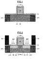
- the reference ZA denotes an active zone of a silicon semiconductor substrate, delimited laterally by STI lateral isolation zones, for example of the type trenched slightly deep.
- lateral isolation regions STI are realized so conventional and known in itself by the skilled person.
- an intermediate layer CI is deposited here formed of a BARC material, in a thickness typically between 1 and 100 nm.
- This CI layer is suitably deposited.
- This inorganic BARC type material has a very low density, typically 1 g / cm 3 .
- FIG. 2 it is carried out (FIG. 2) in a conventional manner and known in self, a deposit of a layer of resin RS that we develop and that we grave locally, so as to discover the intermediate layer CI.
- IMP implantation is implanted into the orifice bounded by the resin block. This IMP implementation is thus done in particular through the horizontal portion of the layer CI, so as to form the LDD regions.
- the lateral offset provided by the vertical portion of the IC layer is here greater than the increase in lateral dispersion related to the increase in the implantation energy necessary for the depth crossing of the IC layer.
- the person skilled in the art will know the to choose, in order to obtain the maximum distribution of dopants a depth of at least 3 to 4 nm, for example 10 nm.
- a lateral dispersion is obtained post-implantation under the reduced gate of about 10 nm compared to a implantation through an equivalent thickness of silicon dioxide (density 2.3 g / cm 3 ) and decreased by about 7 nm compared to a conventional direct implantation in silicon, that is to say without offset spacers.
- PK regions ("pocket" in English). Implantation of these PK regions can be carried out before or after the implantation of LDD zones. These PK regions help to improve the control of short-circuit effects and avoid, in particular, an excessive fall in threshold voltage of the transistor.
- the next step is to remove by plasma etching containing oxygen, the IC layer ( Figure 3) and the resin RS.
- the type of etching for the removal of the CI layer is oxidizing and leads to the formation of a surface oxide OX1.
- a variant of the invention it is possible to proceed at the implantation of the PK zones after removal of the CI layer and before removal of the resin.
- Such a variant makes it possible to implant PK zones in a self-aligned way on the grid while shifting the implantation of LDD zones to control short channel effects and this with the same photolithographic level.
- the rest of the transistor manufacturing process is conventional and known in itself and includes removing the OX1 layer, and then the formation of insulating spacers, for example made of silicon nitride, on the flanks of the grid.
- the BARC type material can be replaced by any low density material (less than silicon dioxide) and capable of to be etched selectively with respect to silicon.
- porous silicon dioxide By way of example, mention may be made of porous silicon dioxide. Such a material also has the advantage of not modifying significantly the conventional fabrication process of a transistor MOS.
Landscapes
- Insulated Gate Type Field-Effect Transistor (AREA)
Abstract
Description
- les figures 1 à 3 illustrent un premier mode de mise en oeuvre d'un procédé selon l'invention, aboutissant à un premier mode de réalisation d'un transistor selon l'invention ; et
- la figure 4 illustre une variante de l'invention.
Claims (14)
- Procédé de fabrication d'un transistor MOS, comprenant une étape de réalisation de régions d'extension de source et de drain comportant la formation d'une région de grille sur un substrat semiconducteur et une implantation de dopants dans le substrat de part et d'autre et à distance de la grille du transistor, caractérisé par le fait que ladite étape de réalisation des régions d'extension de source et de drain comporte la formation d'une couche intermédiaire (CI) sur les flancs de la grille (GR) et sur la surface du substrat, cette couche intermédiaire étant formée d'un matériau moins dense que le dioxyde de silicium, et par le fait que ladite implantation de dopants (IMP) est effectuée à travers la partie de ladite couche intermédiaire située sur le substrat.
- Procédé selon la revendication 1, caractérisé par le fait que le matériau formant la couche intermédiaire (CI) est un matériau anti-réflecteur utilisé comme sous-couche anti-réflectrice lors d'une insolation d'une résine photosensible.
- Procédé selon la revendication 1, caractérisé par le fait que le matériau formant la couche intermédiaire (CI) est du dioxyde de silicium poreux.
- Procédé selon l'une des revendications précédentes, caractérisé par le fait qu'on forme des régions (PK) par implantation oblique de dopants de type opposé à celui utilisé pour les implantations de source, drain et des régions d'extension de source et de drain (LDD), et par le fait qu'on effectue cette implantation oblique à travers la couche intermédiaire.
- Procédé selon l'une des revendications précédentes, caractérisé par le fait que le matériau formant la couche intermédiaire (CI) peut être gravé sélectivement par rapport au silicium, et par le fait qu'on retire ladite couche intermédiaire après ladite implantation de dopants.
- Procédé selon la revendication 5, caractérisé par le fait qu'on forme des régions (PK) par implantation oblique de dopants de type opposé à celui utilisé pour les implantations de source, drain et des régions d'extension de source et de drain (LDD), et par le fait qu'on effectue cette implantation oblique après retrait de la couche intermédiaire.
- Procédé selon la revendication 3, caractérisé par le fait qu'on laisse subsister sur les flancs de la grille (GR) et sur une partie du substrat, une portion (CIR) de la couche intermédiaire après ladite implantation, et par le fait qu'on réalise des régions latérales isolantes s'appuyant sur les flancs de la grille et sur une partie du substrat, ces régions latérales isolantes (ESP) comportant ladite portion résiduelle de couche intermédiaire surmontée d'un autre matériau.
- Procédé selon l'une des revendications précédentes, caractérisé par le fait qu'on choisit l'énergie d'implantation de façon à obtenir un maximum de distribution de dopants à une profondeur d'au moins 3 à 4 nanomètres.
- Procédé selon l'une des revendications précédentes, caractérisé par le fait que la dimension de la grille comptée parallèlement à la longueur du canal est inférieure à 180 nanomètres, par exemple inférieure à 100 nanomètres.
- Circuit intégré comportant au moins un transistor obtenu par le procédé selon l'une des revendications 1 à 9.
- Circuit intégré selon la revendication 10, caractérisé par le fait que le transistor comporte des régions latérales isolantes (ESP) s'appuyant sur les flancs de la grille et sur une partie du substrat, ces régions latérales isolantes comportant une couche intermédiaire (CIR) formée d'un matériau moins dense que le dioxyde de silicium, cette couche intermédiaire étant surmontée d'un autre matériau (CS).
- Circuit intégré selon la revendication 11, caractérisé par le fait que le matériau de la couche intermédiaire (CIR) est du dioxyde de silicium poreux.
- Circuit intégré selon l'une des revendications 10 à 12, caractérisé par le fait que la dimension de la grille du transistor, comptée parallèlement à la longueur du canal, est inférieure à 180 nanomètres.
- Circuit intégré selon la revendication 13, caractérisé par le fait que la dimension de la grille du transistor, comptée parallèlement à la longueur du canal, est inférieure à 100 nanomètres.
Applications Claiming Priority (2)
| Application Number | Priority Date | Filing Date | Title |
|---|---|---|---|
| FR0206870A FR2840453B1 (fr) | 2002-06-04 | 2002-06-04 | Procede de fabrication d'un transistor mos de longueur de grille reduite, et circuit integre comportant un tel transistor |
| FR0206870 | 2002-06-04 |
Publications (2)
| Publication Number | Publication Date |
|---|---|
| EP1369909A1 true EP1369909A1 (fr) | 2003-12-10 |
| EP1369909B1 EP1369909B1 (fr) | 2011-02-02 |
Family
ID=29433315
Family Applications (1)
| Application Number | Title | Priority Date | Filing Date |
|---|---|---|---|
| EP03291262A Expired - Lifetime EP1369909B1 (fr) | 2002-06-04 | 2003-05-27 | Procédé de fabrication d'un transistor MOS de longueur de grille réduite, et circuit intégré comportant un tel transistor |
Country Status (4)
| Country | Link |
|---|---|
| US (1) | US6806156B2 (fr) |
| EP (1) | EP1369909B1 (fr) |
| DE (1) | DE60335930D1 (fr) |
| FR (1) | FR2840453B1 (fr) |
Cited By (1)
| Publication number | Priority date | Publication date | Assignee | Title |
|---|---|---|---|---|
| CN113871451A (zh) * | 2021-09-24 | 2021-12-31 | 华虹半导体(无锡)有限公司 | Dmos器件及其形成方法 |
Families Citing this family (4)
| Publication number | Priority date | Publication date | Assignee | Title |
|---|---|---|---|---|
| KR100468785B1 (ko) * | 2003-02-19 | 2005-01-29 | 삼성전자주식회사 | 포켓영역을 구비하는 모스 전계효과 트랜지스터의 제조방법 |
| US7420233B2 (en) * | 2003-10-22 | 2008-09-02 | Micron Technology, Inc. | Photodiode for improved transfer gate leakage |
| US7585763B2 (en) * | 2005-11-07 | 2009-09-08 | Samsung Electronics Co., Ltd. | Methods of fabricating integrated circuit devices using anti-reflective coating as implant blocking layer |
| US9530864B2 (en) * | 2014-06-25 | 2016-12-27 | Globalfoundries Inc. | Junction overlap control in a semiconductor device using a sacrificial spacer layer |
Citations (4)
| Publication number | Priority date | Publication date | Assignee | Title |
|---|---|---|---|---|
| US5492847A (en) * | 1994-08-01 | 1996-02-20 | National Semiconductor Corporation | Counter-implantation method of manufacturing a semiconductor device with self-aligned anti-punchthrough pockets |
| US5736446A (en) * | 1997-05-21 | 1998-04-07 | Powerchip Semiconductor Corp. | Method of fabricating a MOS device having a gate-side air-gap structure |
| US6274445B1 (en) * | 1999-02-03 | 2001-08-14 | Philips Semi-Conductor, Inc. | Method of manufacturing shallow source/drain junctions in a salicide process |
| GB2362029A (en) * | 1999-10-27 | 2001-11-07 | Lucent Technologies Inc | Multi-layer structure for MOSFET Spacers |
Family Cites Families (9)
| Publication number | Priority date | Publication date | Assignee | Title |
|---|---|---|---|---|
| US5976769A (en) * | 1995-07-14 | 1999-11-02 | Texas Instruments Incorporated | Intermediate layer lithography |
| US6180472B1 (en) * | 1998-07-28 | 2001-01-30 | Matsushita Electrons Corporation | Method for fabricating semiconductor device |
| US6274426B1 (en) * | 1999-02-25 | 2001-08-14 | Taiwan Semiconductor Manufacturing Company | Self-aligned contact process for a crown shaped dynamic random access memory capacitor structure |
| US6277683B1 (en) * | 2000-02-28 | 2001-08-21 | Chartered Semiconductor Manufacturing Ltd. | Method of forming a sidewall spacer and a salicide blocking shape, using only one silicon nitride layer |
| US6642590B1 (en) * | 2000-10-19 | 2003-11-04 | Advanced Micro Devices, Inc. | Metal gate with PVD amorphous silicon layer and barrier layer for CMOS devices and method of making with a replacement gate process |
| US6664143B2 (en) * | 2000-11-22 | 2003-12-16 | North Carolina State University | Methods of fabricating vertical field effect transistors by conformal channel layer deposition on sidewalls |
| US6537860B2 (en) * | 2000-12-18 | 2003-03-25 | Apd Semiconductor, Inc. | Method of fabricating power VLSI diode devices |
| US6448165B1 (en) * | 2000-12-21 | 2002-09-10 | Advanced Micro Devices, Inc. | Method for controlling the amount of trim of a gate structure of a field effect transistor |
| US6727534B1 (en) * | 2001-12-20 | 2004-04-27 | Advanced Micro Devices, Inc. | Electrically programmed MOS transistor source/drain series resistance |
-
2002
- 2002-06-04 FR FR0206870A patent/FR2840453B1/fr not_active Expired - Fee Related
-
2003
- 2003-05-27 EP EP03291262A patent/EP1369909B1/fr not_active Expired - Lifetime
- 2003-05-27 DE DE60335930T patent/DE60335930D1/de not_active Expired - Lifetime
- 2003-06-04 US US10/454,361 patent/US6806156B2/en not_active Expired - Lifetime
Patent Citations (4)
| Publication number | Priority date | Publication date | Assignee | Title |
|---|---|---|---|---|
| US5492847A (en) * | 1994-08-01 | 1996-02-20 | National Semiconductor Corporation | Counter-implantation method of manufacturing a semiconductor device with self-aligned anti-punchthrough pockets |
| US5736446A (en) * | 1997-05-21 | 1998-04-07 | Powerchip Semiconductor Corp. | Method of fabricating a MOS device having a gate-side air-gap structure |
| US6274445B1 (en) * | 1999-02-03 | 2001-08-14 | Philips Semi-Conductor, Inc. | Method of manufacturing shallow source/drain junctions in a salicide process |
| GB2362029A (en) * | 1999-10-27 | 2001-11-07 | Lucent Technologies Inc | Multi-layer structure for MOSFET Spacers |
Cited By (1)
| Publication number | Priority date | Publication date | Assignee | Title |
|---|---|---|---|---|
| CN113871451A (zh) * | 2021-09-24 | 2021-12-31 | 华虹半导体(无锡)有限公司 | Dmos器件及其形成方法 |
Also Published As
| Publication number | Publication date |
|---|---|
| EP1369909B1 (fr) | 2011-02-02 |
| US20040046192A1 (en) | 2004-03-11 |
| FR2840453A1 (fr) | 2003-12-05 |
| US6806156B2 (en) | 2004-10-19 |
| FR2840453B1 (fr) | 2005-06-24 |
| DE60335930D1 (de) | 2011-03-17 |
Similar Documents
| Publication | Publication Date | Title |
|---|---|---|
| EP2009682B1 (fr) | Transistor à effet de champ de type finfet isolé du substrat | |
| EP0426251A1 (fr) | Procédé pour fabriquer un dispositif à transistors MIS ayant une électrode de grille en forme de "T" inversé | |
| EP0420748A1 (fr) | Procédé de fabrication d'un circuit intégré MIS haute tension | |
| EP1391939A1 (fr) | Procede de fabrication d'un transistor a effet de champ de type porte de canal | |
| WO2007092867A2 (fr) | Dispositif à semi-conducteur à couche surélevée pour formation d'un siliciure sur la grille | |
| FR3036530A1 (fr) | Procede de realisation de cellules memoires du type a programmation unique comportant des condensateurs mos et circuit integre correspondant | |
| FR2847383A1 (fr) | Procede de fabrication d'un transistor mos de longueur de grille reduite, et circuit integre comportant un tel transistor | |
| FR3067516A1 (fr) | Realisation de regions semiconductrices dans une puce electronique | |
| EP1369909B1 (fr) | Procédé de fabrication d'un transistor MOS de longueur de grille réduite, et circuit intégré comportant un tel transistor | |
| EP2120258A1 (fr) | Procédé de réalisation d'un transistor a source et drain métalliques | |
| JP4782411B2 (ja) | 半導体装置及びその製造方法 | |
| FR3040538A1 (fr) | Transistor mos et son procede de fabrication | |
| EP0522938B1 (fr) | Procédé de fabrication d'un transistor à effet de champ vertical, et transistor obtenu par ce procédé | |
| EP1328969B1 (fr) | Procédé de formation d'un transistor mos | |
| EP3490007A1 (fr) | Methode de fabrication de couples de transistors cmos de type " fin-fet " a basse temperature | |
| US6867087B2 (en) | Formation of dual work function gate electrode | |
| FR3035265A1 (fr) | Procede de fabrication de transistors soi pour une densite d'integration accrue | |
| CN100508138C (zh) | 制造具有双栅结构的半导体器件的方法 | |
| US7494857B2 (en) | Advanced activation approach for MOS devices | |
| EP1494273A1 (fr) | Procédé d'oxydation de silicium | |
| EP0607075B1 (fr) | Composant électronique semi-conducteur à résistance dynamique négative, méthodes d'utilisation et procédé de fabrication correspondants | |
| KR100249798B1 (ko) | 이온 주입 마스크층을 이용한 얇은 접합층 형성 및 이중 게이트구조의 반도체 소자 제조방법 | |
| EP2479785A1 (fr) | Dispositif à effet de champ muni d'une zone barrière de diffusion de dopants localisée et procédé de réalisation | |
| EP0065464B1 (fr) | Procédé de fabrication de circuits intégrés de type MOS | |
| FR2760130A1 (fr) | Transistor mos a faible resistance de drain |
Legal Events
| Date | Code | Title | Description |
|---|---|---|---|
| PUAI | Public reference made under article 153(3) epc to a published international application that has entered the european phase |
Free format text: ORIGINAL CODE: 0009012 |
|
| AK | Designated contracting states |
Kind code of ref document: A1 Designated state(s): AT BE BG CH CY CZ DE DK EE ES FI FR GB GR HU IE IT LI LU MC NL PT RO SE SI SK TR |
|
| AX | Request for extension of the european patent |
Extension state: AL LT LV MK |
|
| 17P | Request for examination filed |
Effective date: 20040609 |
|
| AKX | Designation fees paid |
Designated state(s): DE FR GB IT |
|
| 17Q | First examination report despatched |
Effective date: 20100219 |
|
| RAP1 | Party data changed (applicant data changed or rights of an application transferred) |
Owner name: STMICROELECTRONICS S.A. Owner name: COMMISSARIAT A L'ENERGIE ATOMIQUE ET AUX ENERGIES |
|
| GRAP | Despatch of communication of intention to grant a patent |
Free format text: ORIGINAL CODE: EPIDOSNIGR1 |
|
| GRAS | Grant fee paid |
Free format text: ORIGINAL CODE: EPIDOSNIGR3 |
|
| GRAA | (expected) grant |
Free format text: ORIGINAL CODE: 0009210 |
|
| AK | Designated contracting states |
Kind code of ref document: B1 Designated state(s): DE FR GB IT |
|
| REG | Reference to a national code |
Ref country code: GB Ref legal event code: FG4D Free format text: NOT ENGLISH |
|
| REF | Corresponds to: |
Ref document number: 60335930 Country of ref document: DE Date of ref document: 20110317 Kind code of ref document: P |
|
| REG | Reference to a national code |
Ref country code: DE Ref legal event code: R096 Ref document number: 60335930 Country of ref document: DE Effective date: 20110317 |
|
| PLBE | No opposition filed within time limit |
Free format text: ORIGINAL CODE: 0009261 |
|
| STAA | Information on the status of an ep patent application or granted ep patent |
Free format text: STATUS: NO OPPOSITION FILED WITHIN TIME LIMIT |
|
| 26N | No opposition filed |
Effective date: 20111103 |
|
| REG | Reference to a national code |
Ref country code: DE Ref legal event code: R097 Ref document number: 60335930 Country of ref document: DE Effective date: 20111103 |
|
| PGFP | Annual fee paid to national office [announced via postgrant information from national office to epo] |
Ref country code: DE Payment date: 20120423 Year of fee payment: 10 |
|
| PGFP | Annual fee paid to national office [announced via postgrant information from national office to epo] |
Ref country code: FR Payment date: 20120625 Year of fee payment: 10 Ref country code: GB Payment date: 20120423 Year of fee payment: 10 |
|
| PGFP | Annual fee paid to national office [announced via postgrant information from national office to epo] |
Ref country code: IT Payment date: 20120421 Year of fee payment: 10 |
|
| GBPC | Gb: european patent ceased through non-payment of renewal fee |
Effective date: 20130527 |
|
| PG25 | Lapsed in a contracting state [announced via postgrant information from national office to epo] |
Ref country code: DE Free format text: LAPSE BECAUSE OF NON-PAYMENT OF DUE FEES Effective date: 20131203 |
|
| PG25 | Lapsed in a contracting state [announced via postgrant information from national office to epo] |
Ref country code: IT Free format text: LAPSE BECAUSE OF NON-PAYMENT OF DUE FEES Effective date: 20130527 |
|
| REG | Reference to a national code |
Ref country code: DE Ref legal event code: R119 Ref document number: 60335930 Country of ref document: DE Effective date: 20131203 |
|
| REG | Reference to a national code |
Ref country code: FR Ref legal event code: ST Effective date: 20140131 |
|
| PG25 | Lapsed in a contracting state [announced via postgrant information from national office to epo] |
Ref country code: GB Free format text: LAPSE BECAUSE OF NON-PAYMENT OF DUE FEES Effective date: 20130527 |
|
| PG25 | Lapsed in a contracting state [announced via postgrant information from national office to epo] |
Ref country code: FR Free format text: LAPSE BECAUSE OF NON-PAYMENT OF DUE FEES Effective date: 20130531 |