EP1367717A1 - Semiconductor switch including isolated MOS-transistors - Google Patents
Semiconductor switch including isolated MOS-transistors Download PDFInfo
- Publication number
- EP1367717A1 EP1367717A1 EP03090167A EP03090167A EP1367717A1 EP 1367717 A1 EP1367717 A1 EP 1367717A1 EP 03090167 A EP03090167 A EP 03090167A EP 03090167 A EP03090167 A EP 03090167A EP 1367717 A1 EP1367717 A1 EP 1367717A1
- Authority
- EP
- European Patent Office
- Prior art keywords
- terminal
- mos transistor
- semiconductor switch
- power supply
- switch apparatus
- Prior art date
- Legal status (The legal status is an assumption and is not a legal conclusion. Google has not performed a legal analysis and makes no representation as to the accuracy of the status listed.)
- Granted
Links
Images







Classifications
-
- H—ELECTRICITY
- H10—SEMICONDUCTOR DEVICES; ELECTRIC SOLID-STATE DEVICES NOT OTHERWISE PROVIDED FOR
- H10D—INORGANIC ELECTRIC SEMICONDUCTOR DEVICES
- H10D84/00—Integrated devices formed in or on semiconductor substrates that comprise only semiconducting layers, e.g. on Si wafers or on GaAs-on-Si wafers
- H10D84/01—Manufacture or treatment
- H10D84/0123—Integrating together multiple components covered by H10D12/00 or H10D30/00, e.g. integrating multiple IGBTs
- H10D84/0126—Integrating together multiple components covered by H10D12/00 or H10D30/00, e.g. integrating multiple IGBTs the components including insulated gates, e.g. IGFETs
- H10D84/0151—Manufacturing their isolation regions
-
- H—ELECTRICITY
- H03—ELECTRONIC CIRCUITRY
- H03K—PULSE TECHNIQUE
- H03K17/00—Electronic switching or gating, i.e. not by contact-making and –breaking
- H03K17/51—Electronic switching or gating, i.e. not by contact-making and –breaking characterised by the components used
- H03K17/56—Electronic switching or gating, i.e. not by contact-making and –breaking characterised by the components used by the use, as active elements, of semiconductor devices
- H03K17/687—Electronic switching or gating, i.e. not by contact-making and –breaking characterised by the components used by the use, as active elements, of semiconductor devices the devices being field-effect transistors
- H03K17/6871—Electronic switching or gating, i.e. not by contact-making and –breaking characterised by the components used by the use, as active elements, of semiconductor devices the devices being field-effect transistors the output circuit comprising more than one controlled field-effect transistor
-
- H—ELECTRICITY
- H10—SEMICONDUCTOR DEVICES; ELECTRIC SOLID-STATE DEVICES NOT OTHERWISE PROVIDED FOR
- H10D—INORGANIC ELECTRIC SEMICONDUCTOR DEVICES
- H10D84/00—Integrated devices formed in or on semiconductor substrates that comprise only semiconducting layers, e.g. on Si wafers or on GaAs-on-Si wafers
- H10D84/01—Manufacture or treatment
- H10D84/02—Manufacture or treatment characterised by using material-based technologies
- H10D84/03—Manufacture or treatment characterised by using material-based technologies using Group IV technology, e.g. silicon technology or silicon-carbide [SiC] technology
- H10D84/038—Manufacture or treatment characterised by using material-based technologies using Group IV technology, e.g. silicon technology or silicon-carbide [SiC] technology using silicon technology, e.g. SiGe
-
- H—ELECTRICITY
- H10—SEMICONDUCTOR DEVICES; ELECTRIC SOLID-STATE DEVICES NOT OTHERWISE PROVIDED FOR
- H10D—INORGANIC ELECTRIC SEMICONDUCTOR DEVICES
- H10D84/00—Integrated devices formed in or on semiconductor substrates that comprise only semiconducting layers, e.g. on Si wafers or on GaAs-on-Si wafers
- H10D84/80—Integrated devices formed in or on semiconductor substrates that comprise only semiconducting layers, e.g. on Si wafers or on GaAs-on-Si wafers characterised by the integration of at least one component covered by groups H10D12/00 or H10D30/00, e.g. integration of IGFETs
- H10D84/82—Integrated devices formed in or on semiconductor substrates that comprise only semiconducting layers, e.g. on Si wafers or on GaAs-on-Si wafers characterised by the integration of at least one component covered by groups H10D12/00 or H10D30/00, e.g. integration of IGFETs of only field-effect components
- H10D84/83—Integrated devices formed in or on semiconductor substrates that comprise only semiconducting layers, e.g. on Si wafers or on GaAs-on-Si wafers characterised by the integration of at least one component covered by groups H10D12/00 or H10D30/00, e.g. integration of IGFETs of only field-effect components of only insulated-gate FETs [IGFET]
-
- H—ELECTRICITY
- H10—SEMICONDUCTOR DEVICES; ELECTRIC SOLID-STATE DEVICES NOT OTHERWISE PROVIDED FOR
- H10D—INORGANIC ELECTRIC SEMICONDUCTOR DEVICES
- H10D86/00—Integrated devices formed in or on insulating or conducting substrates, e.g. formed in silicon-on-insulator [SOI] substrates or on stainless steel or glass substrates
- H10D86/201—Integrated devices formed in or on insulating or conducting substrates, e.g. formed in silicon-on-insulator [SOI] substrates or on stainless steel or glass substrates the substrates comprising an insulating layer on a semiconductor body, e.g. SOI
-
- H—ELECTRICITY
- H10—SEMICONDUCTOR DEVICES; ELECTRIC SOLID-STATE DEVICES NOT OTHERWISE PROVIDED FOR
- H10P—GENERIC PROCESSES OR APPARATUS FOR THE MANUFACTURE OR TREATMENT OF DEVICES COVERED BY CLASS H10
- H10P90/00—Preparation of wafers not covered by a single main group of this subclass, e.g. wafer reinforcement
- H10P90/19—Preparing inhomogeneous wafers
- H10P90/1904—Preparing vertically inhomogeneous wafers
- H10P90/1906—Preparing SOI wafers
-
- H—ELECTRICITY
- H10—SEMICONDUCTOR DEVICES; ELECTRIC SOLID-STATE DEVICES NOT OTHERWISE PROVIDED FOR
- H10W—GENERIC PACKAGES, INTERCONNECTIONS, CONNECTORS OR OTHER CONSTRUCTIONAL DETAILS OF DEVICES COVERED BY CLASS H10
- H10W10/00—Isolation regions in semiconductor bodies between components of integrated devices
- H10W10/01—Manufacture or treatment
- H10W10/031—Manufacture or treatment of isolation regions comprising PN junctions
-
- H—ELECTRICITY
- H10—SEMICONDUCTOR DEVICES; ELECTRIC SOLID-STATE DEVICES NOT OTHERWISE PROVIDED FOR
- H10W—GENERIC PACKAGES, INTERCONNECTIONS, CONNECTORS OR OTHER CONSTRUCTIONAL DETAILS OF DEVICES COVERED BY CLASS H10
- H10W10/00—Isolation regions in semiconductor bodies between components of integrated devices
- H10W10/01—Manufacture or treatment
- H10W10/061—Manufacture or treatment using SOI processes together with lateral isolation, e.g. combinations of SOI and shallow trench isolations
-
- H—ELECTRICITY
- H10—SEMICONDUCTOR DEVICES; ELECTRIC SOLID-STATE DEVICES NOT OTHERWISE PROVIDED FOR
- H10W—GENERIC PACKAGES, INTERCONNECTIONS, CONNECTORS OR OTHER CONSTRUCTIONAL DETAILS OF DEVICES COVERED BY CLASS H10
- H10W10/00—Isolation regions in semiconductor bodies between components of integrated devices
- H10W10/10—Isolation regions comprising dielectric materials
- H10W10/181—Semiconductor-on-insulator [SOI] isolation regions, e.g. buried oxide regions of SOI wafers
-
- H—ELECTRICITY
- H10—SEMICONDUCTOR DEVICES; ELECTRIC SOLID-STATE DEVICES NOT OTHERWISE PROVIDED FOR
- H10W—GENERIC PACKAGES, INTERCONNECTIONS, CONNECTORS OR OTHER CONSTRUCTIONAL DETAILS OF DEVICES COVERED BY CLASS H10
- H10W10/00—Isolation regions in semiconductor bodies between components of integrated devices
- H10W10/30—Isolation regions comprising PN junctions
-
- H—ELECTRICITY
- H03—ELECTRONIC CIRCUITRY
- H03K—PULSE TECHNIQUE
- H03K17/00—Electronic switching or gating, i.e. not by contact-making and –breaking
- H03K17/51—Electronic switching or gating, i.e. not by contact-making and –breaking characterised by the components used
- H03K17/56—Electronic switching or gating, i.e. not by contact-making and –breaking characterised by the components used by the use, as active elements, of semiconductor devices
- H03K17/687—Electronic switching or gating, i.e. not by contact-making and –breaking characterised by the components used by the use, as active elements, of semiconductor devices the devices being field-effect transistors
- H03K17/693—Switching arrangements with several input- or output-terminals, e.g. multiplexers, distributors
-
- H—ELECTRICITY
- H10—SEMICONDUCTOR DEVICES; ELECTRIC SOLID-STATE DEVICES NOT OTHERWISE PROVIDED FOR
- H10W—GENERIC PACKAGES, INTERCONNECTIONS, CONNECTORS OR OTHER CONSTRUCTIONAL DETAILS OF DEVICES COVERED BY CLASS H10
- H10W10/00—Isolation regions in semiconductor bodies between components of integrated devices
- H10W10/01—Manufacture or treatment
- H10W10/011—Manufacture or treatment of isolation regions comprising dielectric materials
- H10W10/012—Manufacture or treatment of isolation regions comprising dielectric materials using local oxidation of silicon [LOCOS]
-
- H—ELECTRICITY
- H10—SEMICONDUCTOR DEVICES; ELECTRIC SOLID-STATE DEVICES NOT OTHERWISE PROVIDED FOR
- H10W—GENERIC PACKAGES, INTERCONNECTIONS, CONNECTORS OR OTHER CONSTRUCTIONAL DETAILS OF DEVICES COVERED BY CLASS H10
- H10W10/00—Isolation regions in semiconductor bodies between components of integrated devices
- H10W10/01—Manufacture or treatment
- H10W10/011—Manufacture or treatment of isolation regions comprising dielectric materials
- H10W10/014—Manufacture or treatment of isolation regions comprising dielectric materials using trench refilling with dielectric materials, e.g. shallow trench isolations
-
- H—ELECTRICITY
- H10—SEMICONDUCTOR DEVICES; ELECTRIC SOLID-STATE DEVICES NOT OTHERWISE PROVIDED FOR
- H10W—GENERIC PACKAGES, INTERCONNECTIONS, CONNECTORS OR OTHER CONSTRUCTIONAL DETAILS OF DEVICES COVERED BY CLASS H10
- H10W10/00—Isolation regions in semiconductor bodies between components of integrated devices
- H10W10/10—Isolation regions comprising dielectric materials
- H10W10/13—Isolation regions comprising dielectric materials formed using local oxidation of silicon [LOCOS], e.g. sealed interface localised oxidation [SILO] or side-wall mask isolation [SWAMI]
-
- H—ELECTRICITY
- H10—SEMICONDUCTOR DEVICES; ELECTRIC SOLID-STATE DEVICES NOT OTHERWISE PROVIDED FOR
- H10W—GENERIC PACKAGES, INTERCONNECTIONS, CONNECTORS OR OTHER CONSTRUCTIONAL DETAILS OF DEVICES COVERED BY CLASS H10
- H10W10/00—Isolation regions in semiconductor bodies between components of integrated devices
- H10W10/10—Isolation regions comprising dielectric materials
- H10W10/17—Isolation regions comprising dielectric materials formed using trench refilling with dielectric materials, e.g. shallow trench isolations
Definitions
- the present invention relates to a semiconductor switch apparatus for radio frequency signals.
- semiconductor switch apparatuses are used for switching the operation of an antenna circuit and a receiving transmitting circuit.
- a prior art semiconductor switch apparatus using GaAs FETs is very simple and therefore, can be constructed by one semiconductor chip. That is, since the GaAs FETs serve as passive elements such as resistors and capacitors, bias circuits for the GaAs FETs are unnecessary. Also, since the substrate of the GaAs switch circuit is made of semi-insulating material of high resistance, the leakage of radio frequency signals via the substrate can be suppressed. This will be explained later in detail.
- the series MOS transistor is formed within a first region of a semiconductor layer on an SOI configuration surrounded by a first trench insulating layer
- the shunt MOS transistor is formed within a second region of the semiconductor layer surrounded by a second trench insulating layer.
- the leakage of radio frequency signals from the series MOS transistor to the shunt MOS transistor can be suppressed by the trench insulating layers.
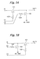
- Fig. 1A which illustrates a first prior art apparatus
- this is of a single pole single throw (SPST) type using GaAs technology which is constructed by a series GaAs FET 101 connected between input terminal IN and output terminal OUT1, and a shunt GaAs FET 102 connected between output terminal OUT1 and AC ground terminal AC-GND.
- control terminals C1 and C2 are connected via gate protection resistors 103 and 104 to the gates of GaAs FETs 101 and 102, respectively.
- shunt FET 102 and gate protection resistor 104 can be connected to input terminal IN.
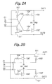
- Fig. 2A which illustrates a second prior art apparatus
- this is of a single pole double throw (SPDT) type using GaAs technology which is further constructed by a series GaAs FET 101' connected between input terminal IN and output terminal OUT2, and a shunt GaAs FET 102' connected between output terminal OUT2 and ground terminal AC-GND in addition to the apparatus of Fig. 1A.
- control terminals C1 and C2 are connected via gate protection resistors 103' and 104' to the gates of GaAs FETs 101' and 102', respectively.
- FETs 101 and 102 When a high voltage such as 3V is applied to control terminal C1 and a low voltage such as 0V is applied to control terminal C2, FETs 101 and 102 are turned ON and OFF, respectively, so that a radio frequency signal can be transmitted from input terminal IN via FET 101 to output terminal OUT1. Simultaneously, FETs 101' and 102' are turned OFF and ON, respectively, so that output terminal OUT2 is completely short-circuited to AC ground terminal AC-GND. Thus, leakage of the radio frequency signal between terminals IN and OUT2 is suppressed, which improves the isolation characteristics of FET 101'.
- shunt FETs 102 and 102' and gate protection resistors 104 and 104' can be connected to input terminal IN.
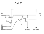
- this circuit is of an SPST type using silicon technology which is constructed by a series MOS transistor 1 connected between an input terminal IN and an output terminal OUT1, and a shunt MOS transistor 2 connected between output terminal OUT1 and an AC ground terminal AC-GND.
- control terminals C1 and C2 are connected via gate protection resistors 3 and 4 to the gates of MOS transistors 1 and 2, respectively.
- the back gates of MOS transistors 1 and 2 are connected to a DC ground terminal DC-GND, that is, the back gates of MOS transistors 1 and 2 are directly grounded.
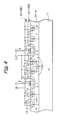
- the apparatus of Fig. 3 is of a conventional CMOS switch configuration illustrated in Fig. 4.
- reference numeral 11 designates a p - -type monocrystalline silicon substrate having a resistivity of about 10 ⁇ ⁇ cm. Also, p-type silicon wells 12-1, 12-2, ⁇ and n-type silicon wells 13-1, 13-2, ⁇ are formed on silicon substrate 11.
- series MOS transistor 1 is formed by a gate silicon oxide layer 14-1, a gate electrode layer 15-1 and n + -type impurity doped regions 16.
- shunt MOS transistor 2 is formed by a gate silicon oxide layer 14-2, a gate electrode layer 15-2 and n + -type impurity doped regions 16.
- n + -type taken-out regions 17 are formed and connected to the DC ground terminal DC-GND, that is, the back gates of MOS transistors 1 and 2 are directly grounded.
- n + -type taken-out regions 18 are formed and connected to DC ground terminal DC-GND.
- radio frequency signals leak from p-type silicon well 12-2 via silicon substrate 11 to p-type silicon well 12-3 as indicated by X in Fig. 4. Also, radio frequency signals leak from p-type silicon well 12-2 via n-type silicon well 13-2 to p-type silicon well 12-3 as indicated by Y in Fig. 4. Further, radio frequency signals leak from p-type silicon wells 12-2 and 12-3 to DC ground terminal DC-GND as indicated by Z in Fig. 4. Thus, transmission loss of radio frequency signals is remarkably large.
- a fourth prior art semiconductor switch apparatus as illustrated in Fig. 5 is known (see: JP-A-2000-294786). That is, a silicon oxide layer 19 is inserted between silicon substrate 11 and silicon wells 12-1, 12-2, ⁇ , 13-1, 13-2, ⁇ of Fig. 4, thus realizing an SOI configuration. As a result, the resistance of silicon substrate 11 across silicon oxide layer 19 is substantially increased and leakage of radio frequency signals via the silicon substrate 11 as indicated by X is Fig. 4 decreases.
- a fifth prior art semiconductor switch apparatus as illustrated in Fig. 6 is known where resistors 20 are inserted between p + -type taken-out regions 17 and DC ground terminal DC-GND of Fig. 4 (see: US. Patent No. 6,094, 088). That is, the back gates of the MOS transistors 1 and 2 are connected via resistors 20 to DC ground terminal UC-GND.
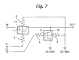
- a resistor 5 is connected between the back gate of MOS transistor 1 and DC ground terminal DC-GND of Fig. 3, and a resistor 6 is connected between the back gate of MOS transistor 2 and DC ground terminal DC-GND of Fig. 3. Note that resistors 5 and 6 correspond to resistor 20 of Fig. 6.
- MOS transistor 1 is isolated by a trench insulating layer T1 from the other elements
- MOS transistor 2 is isolated by a trench insulating layer T2 from the other elements.
- resistors 5 and 6 are as close as possible to MOS transistors 1 and 2, respectively, thus preventing radio frequency signals from superposing each other.
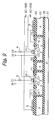
- reference numeral 21 designates a monocrystalline silicon substrate 21 on which a silicon oxide layer 22 is formed. Also, a p-type silicon layer 23 is grown on silicon oxide layer 22, thus realizing an SOI configuration.
- a field silicon oxide layer 24 is formed on silicon layer 23 by a local oxidation of silicon (LOCOS) process.
- LOCOS local oxidation of silicon
- Trench insulating layers T1 and T2 are buried in trenches (grooves) in field silicon oxide layer 24 and silicon layer 23.
- a photoresist pattern for the trenches is formed in field silicon oxide layer 24 and silicon layer 23 by a photolithography process.
- a plasma dry etching process is performed upon field silicon oxide layer 24 and silicon layer 23 using the photoresist pattern as a mask.
- a silicon oxide layer is buried in the trenches.
- a gate insulating layer 25-1, a gate electrode layer 26-1, n + -type impurity doped regions 271S and 271D, and a p + -type taken-out region 28-1 are formed to realize series MOS transistor 1.
- a gate insulating layer 25-2, a gate electrode layer 26-2, n + -type impurity doped regions 272S and 272D, and a p + -type taken-out region 28-2 are formed to realize shunt MOS transistor 2.
- a polycrystalline silicon layer is deposited on field silicon oxide layer 24 and patterned to form resistors 5 and 6 as well as gate protection resistors 3 and 4.
- resistor 5 is inserted between silicon layer 23 surrounded by trench insulating layer T1 and DC ground terminal DC-GND
- resistor 6 is inserted between silicon layer 23 surrounded by layer T2 and DC ground terminal DC-GND
- leakage of radio frequency signals from the silicon layer 23 surrounded by layers T1 and T2 to DC ground terminal DC-GND can be suppressed.
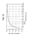
- the resistance value is preferably larger than about 500 ⁇ .
- the operating range of the semiconductor switch circuit depends on the circuit elements connected thereto and the grounding method of DC ground terminal DC-GND, if the resistance value is larger than about 10M ⁇ , the operation of the semiconductor switch apparatus becomes unstable in a DC manner.
- the resistance value of resistors 5 and 6 is preferably about 500 ⁇ to 10M ⁇ .
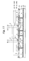
- resistors 5 and 6 are formed by p + -type impurity doped regions in silicon layer 23.
- openings having a predetermined size are perforated in filed silicon oxide layer 24 by a photolithography and etching process, and then, 1E + 15 boron ions/cm 2 are implanted into silicon layer 23 at an energy of 30keV.
- resistor 5 as well as MOS transistor 1 is isolated by trench insulating layer T1
- resistor 6 as well as MOS transistor 2 is isolated by trench insulating layer T2 thus surely preventing radio frequency signals from superposing on each other.
- regions 23a of silicon layer 23 under p + -type taken-out regions 28-1 and 28-2 is made smaller than that of the other region of p + -type taken-out regions 28-1 and 28-2.
- regions 23a serve as resistors 5 and 6 of Figs. 8 and 9.
- n + -type impurity doped region 271S and p + -type taken-out region 18-1 is made longer, and the distance between n + -type impurity doped region 272S and p + -type taken-out region 18-2 is made longer.
- silicon layer 23 per se serves as resistors 5 and 6 of Figs. 8 and 9.
- control voltages applied to control terminals C1 and C2 are usually 0V and 3V. If the control voltages applied to control terminals C1 and C2 are 3V and 0V, respectively, MOS transistors 1 and 2 are expected to be completely turned ON and OFF, respectively. Also, if the amplitude of radio frequency signals applied to the input terminal IN is represented by ⁇ V in , ⁇ V in /2 is applied between the drain and gate of transistor 2. Therefore, if ⁇ V in /2 >V th where V th is a threshold voltage of transistor 2, this would be turned ON.
- a DC/DC converter 31 and a switching circuit 32 constructed by CMOS circuits are added to the elements of Fig. 7, thus surely turning OFF transistor 2. That is, DC/DC converter 31 receives a power supply voltage V DD such as 3V and generates a voltage of -3V. Also, switching circuit 32 receives the power supply voltage V DD (3V) and the voltage -3V from DC/DC converter 31 and generates the control signals (C1 and C2) whose voltages are 3V and -3V in accordance with a voltage applied to a control terminal C.
- V DD power supply voltage
- switching circuit 32 receives the power supply voltage V DD (3V) and the voltage -3V from DC/DC converter 31 and generates the control signals (C1 and C2) whose voltages are 3V and -3V in accordance with a voltage applied to a control terminal C.
- the switching circuit 32 is constructed by p-channel MOS transistors 321 and 322 having a threshold voltage of about 0.5V, N-channel MOS transistors 323 and 324 having a threshold voltage of about 3.5V, and an inverter 325.
- transistors 321, 322, 323 and 324 are turned OFF, ON, ON and OFF respectively.
- the voltages at terminals C1 and C2 are -3V and 3V, respectively, so that transistors 1 and 2 are turned OFF and ON, respectively.
- a DC/DC converter 31' is provided instead of DC/DC converter 31 of Fig. 16. That is, DC/DC converter 31' receives the power supply voltage V DD such as 3V and generates a voltage of 6V. Also, in switching circuit 32, p-channel MOS transistors 321 and 322 have a threshold voltage of about 4V. Additionally, the threshold voltage of N-channel MOS transistors 323 and 324 is made, for example, 1V.
- MOS transistors 321, 322, 323 and 324 When a high voltage such as 3V is applied to control terminal C, transistors 321, 322, 323 and 324 are turned ON, OFF, OFF and ON, respectively. As a result, the voltages at terminals C1 and C2 are 6V and 0V, respectively, so that MOS transistors 1 and 2 are turned ON and OFF, respectively. Therefore, a radio frequency signal can be transmitted from input terminal IN via MOS transistor 1 to output terminal OUT1. In this case, since the threshold voltage of MOS transistor 2 is very high (4V), MOS transistor 2 would not turn ON even if the amplitude of radio frequency signals at input terminal IN is large.
- control terminal C when a low voltage such as 0V is applied to control terminal C, transistors 321, 322, 323 and 324 are turned OFF, ON, ON and OFF respectively. As a result, the voltages at terminals C1 and C2 are 0V and 6V, respectively, so that MOS transistors 1 and 2 are turned OFF and ON, respectively.
- the DC-DC converter 31 or 31' and switching circuit 32 can be applied to the apparatus of Fig. 18.
- Figs. 16 and 17 The layout of the apparatuses of Figs. 16 and 17 is illustrated in Fig. 18, and realized by silicon technology.
- a series MOS transistor 1' along with its gate protection resistor 3' and a resistor 5' is connected in series to series MOS transistor 1 of Fig. 7, and a shunt MOS transistor 2' along with its gate protection resistor 4' and a resistor 6' is connected in series to shunt MOS transistor 2 of Fig. 7.
- each of the MOS transistors 1, 1', 2 and 2' is isolated by trench insulating layers T1 and T2, so that leakage of radio frequency signals from silicon layer 23 of transistor 1 to that of transistor 1' and leakage of radio frequency signals from silicon layer 23 of transistor 2 to that of transistor 2' can be sufficiently suppressed.
- resistors 5 and 5' as well as MOS transistors 1 and 1' are isolated by trench insulating layer T1
- resistors 6 and 6' as well as MOS transistors 2 and 2' are isolated by trench insulating layer T2, thus surely preventing radio frequency signals from superposing on each other.
- resistors 5, 5', 6 and 6' are formed in the same way as in Fig. 14 or 15.
- a series capacitor for DC cut can be externally provided at input terminal IN and output terminal OUT1, and a shunt capacitor for AC cut can be internally provided at transistor 2.
- series capacitors 7 and 8 are connected to input terminal IN and output terminal OUT1, respectively, and a shunt capacitor 9 is connected between transistor 2 and AC ground terminal AC-GND.
- shunt capacitor 9 is constructed by a metal-insulator-metal (MIM) capacitance or a MOS capacitance.
- shunt MOS transistor 2 (2') is connected to output terminal OUT1
- shunt MOS transistor 2 (2') can be connected to input terminal IN (see: Figs. 2A and 2B).
- the leakage of radio frequency signals can be further suppressed, that is, the transmission loss of radio frequency signals can be further suppressed.
Landscapes
- Semiconductor Integrated Circuits (AREA)
- Electronic Switches (AREA)
- Metal-Oxide And Bipolar Metal-Oxide Semiconductor Integrated Circuits (AREA)
- Thin Film Transistor (AREA)
Abstract
Description
- The present invention relates to a semiconductor switch apparatus for radio frequency signals.
- In a mobile communication apparatus such as a mobile telephone apparatus using radio frequency signals such as GHz microwave signals, semiconductor switch apparatuses are used for switching the operation of an antenna circuit and a receiving transmitting circuit.
- A prior art semiconductor switch apparatus using GaAs FETs is very simple and therefore, can be constructed by one semiconductor chip. That is, since the GaAs FETs serve as passive elements such as resistors and capacitors, bias circuits for the GaAs FETs are unnecessary. Also, since the substrate of the GaAs switch circuit is made of semi-insulating material of high resistance, the leakage of radio frequency signals via the substrate can be suppressed. This will be explained later in detail.
- In the above-described prior art semiconductor switch apparatus using GaAs FETs, however, since GaAs substrates are expensive, manufacturing costs are high.
- In another prior art semiconductor switch apparatus using silicon MOS transistors, in order to suppress the leakage of radio frequency signals, a silicon-on-insulator (SOI) configuration is adopted (see: JP-A-2000-294786) or a resistor is inserted between the back gate of each of the MOS transistors and a ground terminal (see: U. S. Patent No. 6, 094, 088). This also will be explained later in detail.
- In the above-described prior art semiconductor switch apparatus using silicon MOS transistors, although the manufacturing cost can be low, leakage of radio frequency signals is still a serious problem also to be explained later in detail.
- It is an object of the invention to provide a semiconductor switch apparatus using silicon MOS transistors capable of further decreasing the transmission loss of radio frequency signals.
- According to the invention, in a semiconductor switch apparatus including an input terminal, an output terminal, an AC ground terminal, a DC ground terminal, at least one series MOS transistor connected between the input terminal and the output terminal, and at least one shunt MOS transistor connected between one of the input terminal and the output terminal and the AC ground terminal, the series MOS transistor is formed within a first region of a semiconductor layer on an SOI configuration surrounded by a first trench insulating layer, and the shunt MOS transistor is formed within a second region of the semiconductor layer surrounded by a second trench insulating layer.
- Thus, the leakage of radio frequency signals from the series MOS transistor to the shunt MOS transistor can be suppressed by the trench insulating layers.
- The invention will be more clearly understood from the description set forth below, as compared with the prior art, with reference to the accompanying drawings, wherein:
- Fig. 1A is an equivalent circuit diagram illustrating a first prior art semiconductor switch apparatus;
- Fig. 1B is an equivalent circuit diagram illustrating a modification of the apparatus of Fig. 1A;
- Fig. 2A is an equivalent circuit diagram illustrating a second prior art semiconductor switch apparatus;
- Fig. 2B is an equivalent circuit diagram illustrating a modification of the apparatus of Fig. 2A;
- Fig. 3 is an equivalent circuit diagram illustrating a third prior art semiconductor switch apparatus;
- Fig. 4 is a cross-sectional view of the apparatus of Fig. 3;
- Fig. 5 is a cross-sectional view illustrating a fourth prior art semiconductor switch apparatus;
- Fig. 6 is a cross-sectional view illustrating a fifth prior art semiconductor switch apparatus;
- Fig. 7 is an equivalent circuit diagram illustrating a first embodiment of the semiconductor switch apparatus according to the invention;
- Fig. 8 is a plan view of the apparatus of Fig. 7;
- Fig. 9 is a cross-sectional view of the apparatus of Fig. 7;
- Fig. 10 is a graph showing the insertion loss characteristics with respect to the resistance value of the resistors of Figs. 8 and 9;
- Fig. 11 is a cross-sectional view illustrating a modification of Fig. 9;
- Fig. 12 is an equivalent circuit diagram illustrating a second embodiment of the semiconductor switch apparatus according to the invention;
- Fig. 13 is a plan view of the apparatus of Fig. 12;
- Fig. 14 is a cross-sectional view of the apparatus of Fig. 12;
- Fig. 15 is a cross-sectional view illustrating a modification of Fig. 14;
- Fig. 16 is an equivalent circuit diagram illustrating a third embodiment of the semiconductor switch apparatus according to the invention;
- Fig. 17 is an equivalent circuit diagram illustrating a modification of Fig. 16;
- Fig. 18 is a layout diagram of the apparatuses of Figs. 16 and 17;
- Fig. 19 is an equivalent circuit diagram illustrating a fourth embodiment of the semiconductor switch apparatus according to the invention;
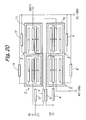
- Fig. 20 is a plan view of the apparatus of Fig. 19;
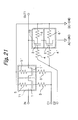
- Fig. 21 is an equivalent circuit diagram illustrating a fifth embodiment of the semiconductor switch apparatus according to the invention;
- Fig. 22 is a plan view of the apparatus of Fig. 21; and
- Fig. 23 is an equivalent circuit diagram illustrating a modification of Fig. 7.
-
- Before the description of the preferred embodiments, prior art semiconductor switch apparatuses will be explained with reference to Figs. 1A, 1B, 2A, 2B, 3, 4, 5 and 6.
- In Fig. 1A, which illustrates a first prior art apparatus, this is of a single pole single throw (SPST) type using GaAs technology which is constructed by a series GaAs FET 101 connected between input terminal IN and output terminal OUT1, and a shunt GaAs FET 102 connected between output terminal OUT1 and AC ground terminal AC-GND. Also, control terminals C1 and C2 are connected via
gate protection resistors - When a high voltage such as 3V is applied to control terminal C1 and a low voltage such as 0V is applied to control terminal C2,
FETs FET 101 to output terminal OUT1. - On the other hand, when a low voltage such as 0V is applied to control terminal C1 and a high voltage such as 3V is applied to control terminal C2,
FETs FET 101. - Note that, as illustrated in Fig. 1B, shunt FET 102 and
gate protection resistor 104 can be connected to input terminal IN. - In Fig. 2A, which illustrates a second prior art apparatus, this is of a single pole double throw (SPDT) type using GaAs technology which is further constructed by a series GaAs FET 101' connected between input terminal IN and output terminal OUT2, and a shunt GaAs FET 102' connected between output terminal OUT2 and ground terminal AC-GND in addition to the apparatus of Fig. 1A. Also, control terminals C1 and C2 are connected via gate protection resistors 103' and 104' to the gates of GaAs FETs 101' and 102', respectively.
- When a high voltage such as 3V is applied to control terminal C1 and a low voltage such as 0V is applied to control terminal C2,
FETs FET 101 to output terminal OUT1. Simultaneously, FETs 101' and 102' are turned OFF and ON, respectively, so that output terminal OUT2 is completely short-circuited to AC ground terminal AC-GND. Thus, leakage of the radio frequency signal between terminals IN and OUT2 is suppressed, which improves the isolation characteristics of FET 101'. - On the other hand, when a low voltage such as 0V is applied to control terminal C1 and a high voltage such as 3V is applied to control terminal C2, FETs 101' and 102' are turned ON and OFF, respectively, so that a radio frequency signal can be transmitted from input terminal IN via FET 101' to output terminal OUT2. Simultaneously,
FETs FET 101. - Note that, as illustrated in Fig. 2B,
shunt FETs 102 and 102' andgate protection resistors 104 and 104' can be connected to input terminal IN. - In Figs. 1A, 1B, 2A and 2B, since
FETs FETs 101, 101' 102 and 102' are unnecessary. Also, since a substrate of GaAs switch circuit is made of semi-insulating material having a high resistance, leakage of radio frequency signals via the substrate can be suppressed. - In the semiconductor switch circuits of Figs. 1A, 1B, 2A and 2B, however, since GaAs substrates are expensive, the manufacturing cost is very high.
- In Fig. 3, which illustrates a third prior art apparatus, this circuit is of an SPST type using silicon technology which is constructed by a
series MOS transistor 1 connected between an input terminal IN and an output terminal OUT1, and ashunt MOS transistor 2 connected between output terminal OUT1 and an AC ground terminal AC-GND. Also, control terminals C1 and C2 are connected viagate protection resistors MOS transistors MOS transistors MOS transistors - The operation is the same as that of the semiconductor switch apparatus of Fig. 1A.
- The apparatus of Fig. 3 is of a conventional CMOS switch configuration illustrated in Fig. 4.
- In Fig. 4,
reference numeral 11 designates a p--type monocrystalline silicon substrate having a resistivity of about 10 Ω ·cm. Also, p-type silicon wells 12-1, 12-2, ··· and n-type silicon wells 13-1, 13-2, ··· are formed onsilicon substrate 11. - In p-type silicon well 12-2,
series MOS transistor 1 is formed by a gate silicon oxide layer 14-1, a gate electrode layer 15-1 and n+-type impurity dopedregions 16. Similarly, in p-type silicon well 12-3,shunt MOS transistor 2 is formed by a gate silicon oxide layer 14-2, a gate electrode layer 15-2 and n+-type impurity dopedregions 16. - Also, in p-type silicon wells 12-1, 12-2, ···, p+-type taken-out
regions 17 are formed and connected to the DC ground terminal DC-GND, that is, the back gates ofMOS transistors regions 18 are formed and connected to DC ground terminal DC-GND. - In Figs. 3 and 4, since the resistivity of
silicon substrate 11 is smaller than that of a GaAs substrate, radio frequency signals leak from p-type silicon well 12-2 viasilicon substrate 11 to p-type silicon well 12-3 as indicated by X in Fig. 4. Also, radio frequency signals leak from p-type silicon well 12-2 via n-type silicon well 13-2 to p-type silicon well 12-3 as indicated by Y in Fig. 4. Further, radio frequency signals leak from p-type silicon wells 12-2 and 12-3 to DC ground terminal DC-GND as indicated by Z in Fig. 4. Thus, transmission loss of radio frequency signals is remarkably large. - In order to suppress leakage of radio frequency signals from p-type silicon well 12-2 via
silicon substrate 11 to p-type silicon well 12-3 as indicated by X in Fig. 4, a fourth prior art semiconductor switch apparatus as illustrated in Fig. 5 is known (see: JP-A-2000-294786). That is, asilicon oxide layer 19 is inserted betweensilicon substrate 11 and silicon wells 12-1, 12-2, ···, 13-1, 13-2, ··· of Fig. 4, thus realizing an SOI configuration. As a result, the resistance ofsilicon substrate 11 acrosssilicon oxide layer 19 is substantially increased and leakage of radio frequency signals via thesilicon substrate 11 as indicated by X is Fig. 4 decreases. - In order to suppress leakage of radio frequency signals from p-type silicon wells 12-2 and 12-3 to DC ground terminal DC-GND as indicated by Z in Fig. 4, a fifth prior art semiconductor switch apparatus as illustrated in Fig. 6 is known where
resistors 20 are inserted between p+-type taken-outregions 17 and DC ground terminal DC-GND of Fig. 4 (see: US. Patent No. 6,094, 088). That is, the back gates of theMOS transistors resistors 20 to DC ground terminal UC-GND. - Thus, even if the apparatus of Fig. 5 is combined with that of Fig. 6, leakage of radio frequency signals from p-type silicon well 12-2 via n-type silicon well 13-2 to p-type silicon well 12-3 as indicated by Y in Fig. 4 will not decrease , so that the transmission loss of radio frequency signals is still large.
- In Fig. 7, which illustrates a first embodiment of the semiconductor switch apparatus according to the invention, a
resistor 5 is connected between the back gate ofMOS transistor 1 and DC ground terminal DC-GND of Fig. 3, and aresistor 6 is connected between the back gate ofMOS transistor 2 and DC ground terminal DC-GND of Fig. 3. Note thatresistors - Also,
MOS transistor 1 is isolated by a trench insulating layer T1 from the other elements, andMOS transistor 2 is isolated by a trench insulating layer T2 from the other elements. In this case,resistors MOS transistors - The apparatus of Fig. 7 will be explained next with reference to Figs. 8 and 9.
- In Fig. 9,
reference numeral 21 designates amonocrystalline silicon substrate 21 on which asilicon oxide layer 22 is formed. Also, a p-type silicon layer 23 is grown onsilicon oxide layer 22, thus realizing an SOI configuration. - A field
silicon oxide layer 24 is formed onsilicon layer 23 by a local oxidation of silicon (LOCOS) process. - Trench insulating layers T1 and T2 are buried in trenches (grooves) in field
silicon oxide layer 24 andsilicon layer 23. For example, a photoresist pattern for the trenches is formed in fieldsilicon oxide layer 24 andsilicon layer 23 by a photolithography process. Then, a plasma dry etching process is performed upon fieldsilicon oxide layer 24 andsilicon layer 23 using the photoresist pattern as a mask. Finally, a silicon oxide layer is buried in the trenches. - In an area surrounded by trench insulating layer T1, a gate insulating layer 25-1, a gate electrode layer 26-1, n+-type impurity doped
regions series MOS transistor 1. Similarly, in an area surrounded by insulating trench layer T2, a gate insulating layer 25-2, a gate electrode layer 26-2, n+-type impurity dopedregions shunt MOS transistor 2. - Further, a polycrystalline silicon layer is deposited on field
silicon oxide layer 24 and patterned to formresistors gate protection resistors - In Figs. 8 and 9, since the SOI configuration is adopted, leakage of radio frequency signals from p-
type silicon layer 23 surrounded by trench insulating layer T1 fortransistor 1 viasilicon substrate 21 to p-type silicon layer 23 surrounded by trench insulating layer T2 fortransistor 2 can be suppressed. - Also, in Figs. 8 and 9, since
transistor 1 is surrounded by trench insulating layer T1 andtransistor 2 is surrounded by trench insulating trench layer T2, leakage of radio frequency signals from p-type silicon layer 23 surrounded by trench insulating layer T1 fortransistor 1 via p-type silicon layer 23 between trench insulating layers T1 and T2 to p-type silicon layer 23 surrounded by the trench insulating layer T2 fortransistor 2 can be suppressed. - Since
resistor 5 is inserted betweensilicon layer 23 surrounded by trench insulating layer T1 and DC ground terminal DC-GND, andresistor 6 is inserted betweensilicon layer 23 surrounded by layer T2 and DC ground terminal DC-GND, leakage of radio frequency signals from thesilicon layer 23 surrounded by layers T1 and T2 to DC ground terminal DC-GND can be suppressed. - As shown in Fig. 10, which shows the insertion loss characteristics (the input to output voltage ratio characteristics) with respect to the resistance value of
resistors resistors - In Fig. 11,
resistors silicon layer 23. For example, openings having a predetermined size are perforated in filedsilicon oxide layer 24 by a photolithography and etching process, and then, 1E + 15 boron ions/cm2 are implanted intosilicon layer 23 at an energy of 30keV. - In Fig. 12,
resistor 5 as well asMOS transistor 1 is isolated by trench insulating layer T1, andresistor 6 as well asMOS transistor 2 is isolated by trench insulating layer T2, thus surely preventing radio frequency signals from superposing on each other. - As illustrated in Figs. 13 and 14 the impurity concentration of
regions 23a ofsilicon layer 23 under p+-type taken-out regions 28-1 and 28-2 is made smaller than that of the other region of p+-type taken-out regions 28-1 and 28-2. Thus,regions 23a serve asresistors - In Fig. 15, instead of providing
regions 23a of Fig. 14, the distance between n+-type impurity dopedregion 271S and p+-type taken-out region 18-1 is made longer, and the distance between n+-type impurity dopedregion 272S and p+-type taken-out region 18-2 is made longer. Thus,silicon layer 23 per se serves asresistors - In Figs. 7 and 12, the control voltages applied to control terminals C1 and C2 are usually 0V and 3V. If the control voltages applied to control terminals C1 and C2 are 3V and 0V, respectively,
MOS transistors transistor 2. Therefore, if Δ Vin/2 >Vth where Vth is a threshold voltage oftransistor 2, this would be turned ON. - In Fig. 16, a DC/
DC converter 31 and aswitching circuit 32 constructed by CMOS circuits are added to the elements of Fig. 7, thus surely turning OFFtransistor 2. That is, DC/DC converter 31 receives a power supply voltage VDD such as 3V and generates a voltage of -3V. Also, switchingcircuit 32 receives the power supply voltage VDD(3V) and the voltage -3V from DC/DC converter 31 and generates the control signals (C1 and C2) whose voltages are 3V and -3V in accordance with a voltage applied to a control terminal C. - The switching
circuit 32 is constructed by p-channel MOS transistors channel MOS transistors inverter 325. - When a high voltage such as 3V is applied to control terminal C,
transistors transistors transistor 1 to terminal OUT1. In this case, since the gate voltage oftransistor 2 is very low (-3V), thetransistor 2 is not turned ON even if the amplitude of radio frequency signals at input terminal IN is large. - On the other hand, when a low voltage such as 0V is applied to control terminal C,
transistors transistors - In Fig. 17, a DC/DC converter 31' is provided instead of DC/
DC converter 31 of Fig. 16. That is, DC/DC converter 31' receives the power supply voltage VDD such as 3V and generates a voltage of 6V. Also, in switchingcircuit 32, p-channel MOS transistors channel MOS transistors - When a high voltage such as 3V is applied to control terminal C,
transistors MOS transistors MOS transistor 1 to output terminal OUT1. In this case, since the threshold voltage ofMOS transistor 2 is very high (4V),MOS transistor 2 would not turn ON even if the amplitude of radio frequency signals at input terminal IN is large. - On the other hand, when a low voltage such as 0V is applied to control terminal C,
transistors MOS transistors - The DC-
DC converter 31 or 31' and switchingcircuit 32 can be applied to the apparatus of Fig. 18. - According to the simulation carried out by the inventor, when the apparatus of Fig. 16 without DC-
DC converter 31 and switchingcircuit 32 was applied to an SPDT switch using four MOS transistors corresponding totransistors DC converter 31 and switchingcircuit 32 is applied to such an SPDT switch, the input power at 0.1 dB compression point was 27.3dBm, thus improving the power characteristics. - The layout of the apparatuses of Figs. 16 and 17 is illustrated in Fig. 18, and realized by silicon technology.
- In Fig. 19, a series MOS transistor 1' along with its gate protection resistor 3' and a resistor 5' is connected in series to
series MOS transistor 1 of Fig. 7, and a shunt MOS transistor 2' along with its gate protection resistor 4' and a resistor 6' is connected in series to shuntMOS transistor 2 of Fig. 7. - In Fig. 19, since
transistors 2 and 2' are connected in series, if the amplitude of radio frequency signals applied to the input terminal IN is represented by Δ Vin, Δ Vin/4 is applied between the drain and gate of eachtransistor 2 and 2'. Therefore, unless Δ Vin/4 >Vth where Vth is a threshold voltage oftransistors 2 and 2', these would not be turned ON under the condition that the voltage at control terminal C2 is 0V. - In Fig. 20, each of the
MOS transistors silicon layer 23 oftransistor 1 to that of transistor 1' and leakage of radio frequency signals fromsilicon layer 23 oftransistor 2 to that of transistor 2' can be sufficiently suppressed. - In Fig. 21,
resistors 5 and 5' as well asMOS transistors 1 and 1' are isolated by trench insulating layer T1, andresistors 6 and 6' as well asMOS transistors 2 and 2' are isolated by trench insulating layer T2, thus surely preventing radio frequency signals from superposing on each other. In this case, as illustrated in Fig. 22 which corresponds to Fig. 13,resistors - In Figs. 19, 20, 21 and 22, note that three or more series MOS transistors can be connected in series and three or more shunt MOS transistors can be connected in series.
- In the above-described embodiments, a series capacitor for DC cut can be externally provided at input terminal IN and output terminal OUT1, and a shunt capacitor for AC cut can be internally provided at
transistor 2. For example, in the semiconductor switch apparatus of Fig. 7,series capacitors shunt capacitor 9 is connected betweentransistor 2 and AC ground terminal AC-GND. In this case,shunt capacitor 9 is constructed by a metal-insulator-metal (MIM) capacitance or a MOS capacitance. - Additionally, although the above-described embodiments relate to a SPST switch, the invention can be easily applied to a SPDT switch which is constructed by two SPST switches (see: Figs. 1B and 2B).
- Further, in the above-described embodiments, although shunt MOS transistor 2 (2') is connected to output terminal OUT1, shunt MOS transistor 2 (2') can be connected to input terminal IN (see: Figs. 2A and 2B).
- As explained hereinabove, according to the present invention, since a series MOS transistor and a shunt MOS transistor are isolated by trench insulating layers, the leakage of radio frequency signals can be further suppressed, that is, the transmission loss of radio frequency signals can be further suppressed.
Claims (11)
- A semiconductor switch apparatus comprising:an input terminal (IN);an output terminal (OUT1);an AC ground terminal (AC-GND);a DC ground terminal (DC-GND);at least one series MOS transistor (1, 1') connected between said input terminal and said output terminal; andat least one shunt MOS transistor (2, 2') connected between one of said input terminal and said output terminal and said AC ground terminal, said shunt MOS transistor being operated complementarily with said series MOS transistor;a semiconductor substrate (21);an insulating layer (22) formed on said semiconductor substrate;a semiconductor layer (23) formed on said insulating layer;said series MOS transistor being formed within a first region of said semiconductor layer surrounded by a first trench insulating layer (T1),said shunt MOS transistor being formed within a second region of said semiconductor layer surrounded by a second trench insulating layer (T2).
- The semiconductor switch apparatus as set forth in claim 1, further comprising:at least one first resistor (5, 5') connected between a back gate of said series MOS transistor and said DC ground terminal; andat least one second resistor (6, 6') connected between a back gate of said shunt MOS transistor and said DC ground terminal.
- The semiconductor switch apparatus as set forth in claim 2, wherein a resistance value of each said first and second resistors is about 500Ω to 10MΩ.
- The semiconductor switch apparatus as set forth in claim 2, wherein said first resistor is located outside of said first trench insulating layer, and
said second resistor is located outside of said second trench insulating layer. - The semiconductor switch apparatus as set forth in claim 2, wherein said first resistor is located inside of said first trench insulating layer, and
said second resistor is located inside of said second trench insulating layer. - The semiconductor switch apparatus as set forth in claim 5, wherein said first resistor comprises a low-impurity concentration region within the first region of said semiconductor layer, and said second resistor comprises a low impurity concentration region within the second region of said semiconductor layer.
- The semiconductor switch apparatus as set forth in claim 5, wherein said first resistor comprises a long distance region from said series MOS transistor within the first region of said semiconductor layer, and said second resistor comprises a long distance region from said shunt MOS transistor within the second region of said semiconductor layer.
- The semiconductor switch apparatus as set forth in claim 1, further comprising:a control terminal (C);a power supply terminal (VDD) for generating a first power supply voltage;a DC/DC converter (31), connected to said power supply terminal, for generating a second power supply voltage; anda switching circuit (32), connected to said control terminal, said power supply terminal and said DC/DC converter, for generating first and second complementary control signals (C1, C2) in accordance with a voltage at said control terminal and transmit said first and second complementary control signals to gates of said series MOS transistor and said shunt MOS transistor, respectively,one of said first and second complementary control signals being said first power supply voltage, the other of said first and second complementary control signals being said second power supply voltage.
- The semiconductor switch apparatus as set forth in claim 1, further comprising:a control terminal (C);a power supply terminal (VDD) for generating a first power supply voltage;a DC/DC converter (31), connected to said power supply terminal, for generating a second power supply voltage; anda switching circuit (32), connected to said control terminal, said DC/DC converter and said DC ground terminal, for generating first and second complementary control signals (C1, C2) in accordance with a voltage at said control terminal and transmitting said first and second complementary control signals to gates of said series MOS transistor and said shunt MOS transistor, respectively,one of said first and second complementary control signals being said second power supply voltage, the other of said first and second complementary control signals being a voltage at said DC ground terminal.
- The semiconductor switch apparatus as set forth in claim 1, being a single pole single throw type switch.
- The semiconductor switch apparatus as set forth in claim 1, being a single pole double throw type switch.
Applications Claiming Priority (2)
| Application Number | Priority Date | Filing Date | Title |
|---|---|---|---|
| JP2002156602 | 2002-05-30 | ||
| JP2002156602A JP4262933B2 (en) | 2002-05-30 | 2002-05-30 | High frequency circuit element |
Publications (2)
| Publication Number | Publication Date |
|---|---|
| EP1367717A1 true EP1367717A1 (en) | 2003-12-03 |
| EP1367717B1 EP1367717B1 (en) | 2005-12-21 |
Family
ID=29417212
Family Applications (1)
| Application Number | Title | Priority Date | Filing Date |
|---|---|---|---|
| EP03090167A Expired - Lifetime EP1367717B1 (en) | 2002-05-30 | 2003-05-30 | Semiconductor switch including isolated MOS-transistors |
Country Status (4)
| Country | Link |
|---|---|
| US (1) | US6836172B2 (en) |
| EP (1) | EP1367717B1 (en) |
| JP (1) | JP4262933B2 (en) |
| DE (1) | DE60302831T2 (en) |
Cited By (2)
| Publication number | Priority date | Publication date | Assignee | Title |
|---|---|---|---|---|
| CN100388489C (en) * | 2004-12-31 | 2008-05-14 | 络达科技股份有限公司 | Switching circuit |
| CN103137620A (en) * | 2011-12-05 | 2013-06-05 | Nxp股份有限公司 | Integrated circuit and IC manufacturing method |
Families Citing this family (41)
| Publication number | Priority date | Publication date | Assignee | Title |
|---|---|---|---|---|
| US6804502B2 (en) | 2001-10-10 | 2004-10-12 | Peregrine Semiconductor Corporation | Switch circuit and method of switching radio frequency signals |
| DE102004027361B4 (en) * | 2004-06-04 | 2009-06-10 | Rohde & Schwarz Gmbh & Co. Kg | High frequency switch with extended amplitude and sound dynamics |
| JP4659826B2 (en) | 2004-06-23 | 2011-03-30 | ペレグリン セミコンダクター コーポレーション | RF front-end integrated circuit |
| JP2006332416A (en) | 2005-05-27 | 2006-12-07 | Nec Electronics Corp | Semiconductor device |
| JP5112620B2 (en) * | 2005-05-31 | 2013-01-09 | オンセミコンダクター・トレーディング・リミテッド | Compound semiconductor device |
| USRE48965E1 (en) | 2005-07-11 | 2022-03-08 | Psemi Corporation | Method and apparatus improving gate oxide reliability by controlling accumulated charge |
| US8742502B2 (en) | 2005-07-11 | 2014-06-03 | Peregrine Semiconductor Corporation | Method and apparatus for use in improving linearity of MOSFETs using an accumulated charge sink-harmonic wrinkle reduction |
| US7890891B2 (en) | 2005-07-11 | 2011-02-15 | Peregrine Semiconductor Corporation | Method and apparatus improving gate oxide reliability by controlling accumulated charge |
| US20080076371A1 (en) | 2005-07-11 | 2008-03-27 | Alexander Dribinsky | Circuit and method for controlling charge injection in radio frequency switches |
| US7910993B2 (en) | 2005-07-11 | 2011-03-22 | Peregrine Semiconductor Corporation | Method and apparatus for use in improving linearity of MOSFET's using an accumulated charge sink |
| US9653601B2 (en) | 2005-07-11 | 2017-05-16 | Peregrine Semiconductor Corporation | Method and apparatus for use in improving linearity of MOSFETs using an accumulated charge sink-harmonic wrinkle reduction |
| JP2008071796A (en) * | 2006-09-12 | 2008-03-27 | Toshiba Corp | Semiconductor device and manufacturing method of semiconductor device |
| US7890063B2 (en) * | 2006-10-03 | 2011-02-15 | Samsung Electro-Mechanics | Systems, methods, and apparatuses for complementary metal oxide semiconductor (CMOS) antenna switches using body switching in multistacking structure |
| US7843280B2 (en) * | 2006-12-01 | 2010-11-30 | Samsung Electro-Mechanics Company | Systems, methods, and apparatuses for high power complementary metal oxide semiconductor (CMOS) antenna switches using body switching and substrate junction diode controlling in multistacking structure |
| US20080217727A1 (en) * | 2007-03-11 | 2008-09-11 | Skyworks Solutions, Inc. | Radio frequency isolation for SOI transistors |
| JP4342569B2 (en) * | 2007-04-17 | 2009-10-14 | 株式会社東芝 | High frequency switch circuit |
| US7960772B2 (en) | 2007-04-26 | 2011-06-14 | Peregrine Semiconductor Corporation | Tuning capacitance to enhance FET stack voltage withstand |
| US7738841B2 (en) * | 2007-09-14 | 2010-06-15 | Samsung Electro-Mechanics | Systems, methods and apparatuses for high power complementary metal oxide semiconductor (CMOS) antenna switches using body switching and external component in multi-stacking structure |
| JP5450955B2 (en) * | 2007-12-26 | 2014-03-26 | 株式会社東芝 | High frequency switch |
| JP5417346B2 (en) | 2008-02-28 | 2014-02-12 | ペレグリン セミコンダクター コーポレーション | Method and apparatus for use in digitally tuning a capacitor in an integrated circuit element |
| US8723260B1 (en) | 2009-03-12 | 2014-05-13 | Rf Micro Devices, Inc. | Semiconductor radio frequency switch with body contact |
| JP2010272749A (en) * | 2009-05-22 | 2010-12-02 | Murata Mfg Co Ltd | Semiconductor device |
| US8058922B2 (en) * | 2009-07-28 | 2011-11-15 | Qualcomm, Incorporated | Switch with improved biasing |
| WO2011015903A1 (en) | 2009-08-06 | 2011-02-10 | Freescale Semiconductor, Inc. | Electronic device with protection circuit |
| JP2011176057A (en) * | 2010-02-23 | 2011-09-08 | Panasonic Corp | Semiconductor device |
| JP5135374B2 (en) | 2010-03-24 | 2013-02-06 | 株式会社東芝 | Capacitor, integrated device, high-frequency switching device, and electronic equipment |
| US9590674B2 (en) | 2012-12-14 | 2017-03-07 | Peregrine Semiconductor Corporation | Semiconductor devices with switchable ground-body connection |
| JP5865275B2 (en) | 2013-01-25 | 2016-02-17 | 株式会社東芝 | High frequency semiconductor switch |
| US20150236748A1 (en) | 2013-03-14 | 2015-08-20 | Peregrine Semiconductor Corporation | Devices and Methods for Duplexer Loss Reduction |
| US9406695B2 (en) | 2013-11-20 | 2016-08-02 | Peregrine Semiconductor Corporation | Circuit and method for improving ESD tolerance and switching speed |
| JP5685664B2 (en) * | 2014-04-24 | 2015-03-18 | 株式会社東芝 | Semiconductor switch |
| JP2015226262A (en) * | 2014-05-29 | 2015-12-14 | 株式会社東芝 | Semiconductor switch, wireless device, and semiconductor switch design method |
| TWI645534B (en) * | 2015-03-06 | 2018-12-21 | 聯華電子股份有限公司 | Semiconductor electrostatic discharge protection component |
| US9831857B2 (en) | 2015-03-11 | 2017-11-28 | Peregrine Semiconductor Corporation | Power splitter with programmable output phase shift |
| US9948281B2 (en) | 2016-09-02 | 2018-04-17 | Peregrine Semiconductor Corporation | Positive logic digitally tunable capacitor |
| US10211830B2 (en) | 2017-04-28 | 2019-02-19 | Qualcomm Incorporated | Shunt termination path |
| US10886911B2 (en) | 2018-03-28 | 2021-01-05 | Psemi Corporation | Stacked FET switch bias ladders |
| US10505530B2 (en) | 2018-03-28 | 2019-12-10 | Psemi Corporation | Positive logic switch with selectable DC blocking circuit |
| US10236872B1 (en) | 2018-03-28 | 2019-03-19 | Psemi Corporation | AC coupling modules for bias ladders |
| KR102583788B1 (en) * | 2018-07-09 | 2023-09-26 | 삼성전기주식회사 | Radio frequency switch device of leakage current reduction type |
| US11476849B2 (en) | 2020-01-06 | 2022-10-18 | Psemi Corporation | High power positive logic switch |
Citations (2)
| Publication number | Priority date | Publication date | Assignee | Title |
|---|---|---|---|---|
| US5818099A (en) * | 1996-10-03 | 1998-10-06 | International Business Machines Corporation | MOS high frequency switch circuit using a variable well bias |
| EP0903855A1 (en) * | 1997-02-24 | 1999-03-24 | Sanyo Electric Co., Ltd. | High frequency switching device |
Family Cites Families (6)
| Publication number | Priority date | Publication date | Assignee | Title |
|---|---|---|---|---|
| JP3344598B2 (en) * | 1993-11-25 | 2002-11-11 | 株式会社デンソー | Semiconductor nonvolatile memory device |
| JP2964975B2 (en) | 1997-02-26 | 1999-10-18 | 日本電気株式会社 | High frequency switch circuit |
| US6355537B1 (en) * | 1999-02-23 | 2002-03-12 | Silicon Wave, Inc. | Method of providing radio frequency isolation of device mesas using guard ring regions within an integrated circuit device |
| US6627954B1 (en) * | 1999-03-19 | 2003-09-30 | Silicon Wave, Inc. | Integrated circuit capacitor in a silicon-on-insulator integrated circuit |
| JP2000294786A (en) | 1999-04-05 | 2000-10-20 | Nippon Telegr & Teleph Corp <Ntt> | High frequency switch |
| US6172378B1 (en) * | 1999-05-03 | 2001-01-09 | Silicon Wave, Inc. | Integrated circuit varactor having a wide capacitance range |
-
2002
- 2002-05-30 JP JP2002156602A patent/JP4262933B2/en not_active Expired - Fee Related
-
2003
- 2003-05-22 US US10/443,007 patent/US6836172B2/en not_active Expired - Fee Related
- 2003-05-30 EP EP03090167A patent/EP1367717B1/en not_active Expired - Lifetime
- 2003-05-30 DE DE60302831T patent/DE60302831T2/en not_active Expired - Lifetime
Patent Citations (2)
| Publication number | Priority date | Publication date | Assignee | Title |
|---|---|---|---|---|
| US5818099A (en) * | 1996-10-03 | 1998-10-06 | International Business Machines Corporation | MOS high frequency switch circuit using a variable well bias |
| EP0903855A1 (en) * | 1997-02-24 | 1999-03-24 | Sanyo Electric Co., Ltd. | High frequency switching device |
Non-Patent Citations (1)
| Title |
|---|
| HISANORI UDA ET AL: "HIGH-PERFORMANCE GAAS SWITCH IC'S FABRICATED USING MESFET'S WITH TWO KINDS OF PINCH-OFF VOLTAGES AND A SYMMETRICAL PATTERN CONFIGURATION", IEEE JOURNAL OF SOLID-STATE CIRCUITS, IEEE INC. NEW YORK, US, vol. 29, no. 10, 1 October 1994 (1994-10-01), pages 1262 - 1269, XP000445356, ISSN: 0018-9200 * |
Cited By (5)
| Publication number | Priority date | Publication date | Assignee | Title |
|---|---|---|---|---|
| CN100388489C (en) * | 2004-12-31 | 2008-05-14 | 络达科技股份有限公司 | Switching circuit |
| CN103137620A (en) * | 2011-12-05 | 2013-06-05 | Nxp股份有限公司 | Integrated circuit and IC manufacturing method |
| EP2602817A1 (en) * | 2011-12-05 | 2013-06-12 | Nxp B.V. | Integrated circuit and IC manufacturing method |
| US8847347B2 (en) | 2011-12-05 | 2014-09-30 | Nxp B.V. | Integrated circuit and IC manufacturing method |
| CN103137620B (en) * | 2011-12-05 | 2016-02-24 | Nxp股份有限公司 | Integrated circuit and IC manufacture method |
Also Published As
| Publication number | Publication date |
|---|---|
| DE60302831D1 (en) | 2006-01-26 |
| JP2003347553A (en) | 2003-12-05 |
| DE60302831T2 (en) | 2006-08-31 |
| US20030222704A1 (en) | 2003-12-04 |
| EP1367717B1 (en) | 2005-12-21 |
| US6836172B2 (en) | 2004-12-28 |
| JP4262933B2 (en) | 2009-05-13 |
Similar Documents
| Publication | Publication Date | Title |
|---|---|---|
| EP1367717B1 (en) | Semiconductor switch including isolated MOS-transistors | |
| US11206017B2 (en) | Switch circuit and method of switching radio frequency signals | |
| US7215206B2 (en) | Stacked RF power amplifier | |
| US5786617A (en) | High voltage charge pump using low voltage type transistors | |
| KR100322432B1 (en) | Switched body soi(silicon on insulator) circuits and fabrication method therefor | |
| US20020063270A1 (en) | High frequency switch circuit device | |
| US6853040B2 (en) | MOS transistor and fabrication method thereof | |
| US9318487B2 (en) | High performance power cell for RF power amplifier | |
| US7613442B1 (en) | Switch circuit and method of switching radio frequency signals | |
| TWI681532B (en) | Circuits having a switch with back-gate bias | |
| WO2007124413A2 (en) | Drive circuit and drain extended transistor for use therein | |
| US7112867B2 (en) | Resistive isolation between a body and a body contact | |
| EP3940958B1 (en) | High isolation radio frequency switch | |
| US6433389B1 (en) | Silicon on insulator logic circuit utilizing diode switching elements | |
| EP3945676B1 (en) | High isolation radio frequency multiplexer | |
| CN116317961B (en) | Back gate controlled power amplifier | |
| CN213783275U (en) | Single-pole double-throw switch, signal processing circuit and electronic equipment | |
| CN112564683A (en) | Single-pole double-throw switch, signal processing circuit and electronic equipment | |
| WO2001097289A1 (en) | Silicon on insulator logic circuit utilizing diode switching elements |
Legal Events
| Date | Code | Title | Description |
|---|---|---|---|
| PUAI | Public reference made under article 153(3) epc to a published international application that has entered the european phase |
Free format text: ORIGINAL CODE: 0009012 |
|
| AK | Designated contracting states |
Kind code of ref document: A1 Designated state(s): AT BE BG CH CY CZ DE DK EE ES FI FR GB GR HU IE IT LI LU MC NL PT RO SE SI SK TR |
|
| AX | Request for extension of the european patent |
Extension state: AL LT LV MK |
|
| 17P | Request for examination filed |
Effective date: 20031117 |
|
| AKX | Designation fees paid |
Designated state(s): DE FR NL |
|
| GRAP | Despatch of communication of intention to grant a patent |
Free format text: ORIGINAL CODE: EPIDOSNIGR1 |
|
| GRAS | Grant fee paid |
Free format text: ORIGINAL CODE: EPIDOSNIGR3 |
|
| GRAA | (expected) grant |
Free format text: ORIGINAL CODE: 0009210 |
|
| AK | Designated contracting states |
Kind code of ref document: B1 Designated state(s): DE FR NL |
|
| REF | Corresponds to: |
Ref document number: 60302831 Country of ref document: DE Date of ref document: 20060126 Kind code of ref document: P |
|
| RAP2 | Party data changed (patent owner data changed or rights of a patent transferred) |
Owner name: NEC ELECTRONICS CORPORATION |
|
| NLT2 | Nl: modifications (of names), taken from the european patent patent bulletin |
Owner name: NEC ELECTRONICS CORPORATION Effective date: 20060621 |
|
| ET | Fr: translation filed | ||
| NLS | Nl: assignments of ep-patents |
Owner name: NEC ELECTRONICS CORPORATION Effective date: 20060724 |
|
| PLBE | No opposition filed within time limit |
Free format text: ORIGINAL CODE: 0009261 |
|
| STAA | Information on the status of an ep patent application or granted ep patent |
Free format text: STATUS: NO OPPOSITION FILED WITHIN TIME LIMIT |
|
| 26N | No opposition filed |
Effective date: 20060922 |
|
| REG | Reference to a national code |
Ref country code: NL Ref legal event code: TD Effective date: 20100715 |
|
| REG | Reference to a national code |
Ref country code: FR Ref legal event code: CD |
|
| REG | Reference to a national code |
Ref country code: DE Ref legal event code: R082 Ref document number: 60302831 Country of ref document: DE Representative=s name: STORK BAMBERGER PATENTANWAELTE, DE |
|
| REG | Reference to a national code |
Ref country code: DE Ref legal event code: R082 Ref document number: 60302831 Country of ref document: DE Representative=s name: STORK BAMBERGER PATENTANWAELTE, DE Effective date: 20120828 Ref country code: DE Ref legal event code: R081 Ref document number: 60302831 Country of ref document: DE Owner name: RENESAS ELECTRONICS CORPORATION, JP Free format text: FORMER OWNER: NEC ELECTRONICS CORP., KAWASAKI, JP Effective date: 20120828 Ref country code: DE Ref legal event code: R081 Ref document number: 60302831 Country of ref document: DE Owner name: RENESAS ELECTRONICS CORPORATION, KAWASAKI-SHI, JP Free format text: FORMER OWNER: NEC ELECTRONICS CORP., KAWASAKI, KANAGAWA, JP Effective date: 20120828 Ref country code: DE Ref legal event code: R082 Ref document number: 60302831 Country of ref document: DE Representative=s name: STORK BAMBERGER PATENTANWAELTE PARTMBB, DE Effective date: 20120828 |
|
| REG | Reference to a national code |
Ref country code: FR Ref legal event code: PLFP Year of fee payment: 13 |
|
| PGFP | Annual fee paid to national office [announced via postgrant information from national office to epo] |
Ref country code: DE Payment date: 20150527 Year of fee payment: 13 |
|
| PGFP | Annual fee paid to national office [announced via postgrant information from national office to epo] |
Ref country code: NL Payment date: 20150409 Year of fee payment: 13 Ref country code: FR Payment date: 20150508 Year of fee payment: 13 |
|
| REG | Reference to a national code |
Ref country code: DE Ref legal event code: R119 Ref document number: 60302831 Country of ref document: DE |
|
| REG | Reference to a national code |
Ref country code: NL Ref legal event code: MM Effective date: 20160601 |
|
| PG25 | Lapsed in a contracting state [announced via postgrant information from national office to epo] |
Ref country code: NL Free format text: LAPSE BECAUSE OF NON-PAYMENT OF DUE FEES Effective date: 20160601 |
|
| REG | Reference to a national code |
Ref country code: FR Ref legal event code: ST Effective date: 20170131 |
|
| PG25 | Lapsed in a contracting state [announced via postgrant information from national office to epo] |
Ref country code: FR Free format text: LAPSE BECAUSE OF NON-PAYMENT OF DUE FEES Effective date: 20160531 Ref country code: DE Free format text: LAPSE BECAUSE OF NON-PAYMENT OF DUE FEES Effective date: 20161201 |