Background of the Invention:
-
The present invention relates to a data transfer apparatus
which is effective for a case of transferring comparatively large
capacity data by a comparatively unreliable interface, for example,
a case of reading data out of a memory, writing data into the
memory, or transferring address of the memory.
-
While ranges of use of information processing apparatus,
such as a computer, and the like have been enlarged, processing
speed of these apparatus have been improved. Under the
circumstances, chances in which large capacity data are processed
by those apparatus have also been increased. Especially in a
system having a large constitution, when the large capacity data are
transferred between apparatus, errors are apt to be caused to occur
at the same time over a plurality of bits. Accordingly, desired is a
reliable data transfer apparatus capable of relieving such errors
simultaneously generated over a plurality of bits.
-
Even in a conventional data transfer apparatus, some
countermeasures are taken, in a case that the errors are
simultaneously generated over a plurality of bits and thereby
correction of the errors becomes impossible. Namely, a
countermeasure is taken so that a system carrying out the data
transfer may be immediately stopped and then reasons of the errors
may be checked. Further, another countermeasure is taken so that
the corresponding data may be re-issued from a data output section
or data stored in a shunting buffer, such as a re-sending buffer, or
the like may be re-issued.
-
Moreover, yet another countermeasure is taken as follows,
in a technique disclosed in an official gazette of unexamined
Japanese patent publication, No.2000-244530. Namely, data to be
transmitted are divided into a plurality of data each having a
predetermined quantity of data and then the divided data are stored
in a plurality of sending buffers, respectively. Further, each
storing address of these data is memorized by an address
memorizing means. Accordingly, in a case that data are
transmitted to a transmission destination by a transmission means
and then errors are detected, a sending buffer corresponding to the
erroneous data is deduced from the address memorizing means and
thereby transmission data are re-sent from the deduced sending
buffer.
-
However, in the countermeasure that the system is
checked as soon as the correction of the errors becomes impossible,
the system is unconditionally stopped for a predetermined time to
carry out the check of the system. As a result, a problem of
deterioration of reliability is inevitably caused to occur by
interruption of the data in a system that data transfer needs to be
continuously carried out.
-
Further, in the countermeasure that the corresponding
data are re-issued from the data output section, during the re-issue,
progress of transmission of the data to be re-issued is, of course,
delayed by the time for the re-issue itself. However, the
countermeasure has a problem that progress of transmission of data
other than the re-issue data is delayed similarly to that. For
example, it is assumed that two kinds of data, namely, data to be
sent to a predetermined memory and data to be sent to a
predetermined input device, and that a trouble is caused to occur in
the data sent to the predetermined memory. In this case, the data
to be sent to the predetermined memory are interrupted into data to
be outputted in the data output section. As a result, under the
influence thereof, progress of transmission of the data to be sent to
the predetermined input device is also delayed by the time for the
interruption. Similar problem is also caused to occur in the
technique disclosed in the official gazette of unexamined Japanese
patent publication, No.2000-244530. Accordingly, in these
techniques, as regards data having no relation with the troubled
data and desired to be transmitted without delay, a problem of
deterioration of reliability of the data transfer is inevitably caused
to occur.
-
In order to avoid such a problem, as mentioned before, a
proposal is made about the countermeasure that the data are
re-sent from the shunting buffer by way of a transmission route
different from the data output section. However, in this proposal,
it is necessary to prepare not only a special buffer, that is, the
shunting buffer but also a special transmission route. As a result,
the proposal has a problem that cost of the system is increased by
increase of quantity of hardware. In addition, in a case that the
corresponding data are re-issued from the shunting buffer at the
time of generation of trouble, it is difficult to recognize boundary of
the data, order of transferring the data, and the like. Therefore,
the re-sent data cannot be recognized correctly in the transmission
destination. This sometimes brings about such a phenomenon that,
what is called, transformation of characters is caused to occur.
Sumary of the Invention:
-
It is therefore an object of the present invention to provide
a data transfer apparatus which is, even though predetermined
data are required to be re-sent, capable of preventing transmission
of the other data having no relation with the predetermined data
from being thereby delayed.
-
Other objects of the present invention will become clear as
the description proceeds.
-
According to an aspect of the present invention, there is
provided a data transfer apparatus comprising:
- a plurality of data storing means for storing data of which
transmission timing must not be influenced by delay of
transmission timing of the other data at least with the data being
stored separately to each other;
- data selecting means for selecting data per one unit one by one
at predetermined frequency and order with respect to said a
plurality of data storing means, respectively;
- data transmitting means for transmitting said data selected by
said data selecting means in synchronization with predetermined
clocks one by one per each one clock;
- data receiving means for receiving said data transmitted by
said data transmitting means;
- trouble judging means for checking said data received by said
data receiving means per each one clock and judging whether or not
an uncorrectable trouble is generated in said data of per said each
one clock; and
- re-sending instructing means for instructing, when said trouble
judging means judges that said uncorrectable trouble is generated
in said data of per said each one dock, re-sending of said data of
said one unit including at least said data of per said each one clock
to a corresponding one of said a plurality of data storing means.
-
-
According to another aspect of the present invention,
there is also provided a data transfer apparatus comprising:
- a plurality of data storing means for storing data of which
transmission timing must not be influenced by delay of
transmission timing of the other data at least with the data being
stored separately to each other;
- data selecting means for selecting data per one unit one by one
at predetermined frequency and order with respect to said a
plurality of data storing means, respectively;
- data transmitting means for transmitting said data selected by
said data selecting means in synchronization with predetermined
clocks one by one per each one clock;
- data receiving means for receiving said data transmitted by
said data transmitting means;
- trouble judging means for checking said data received by said
data receiving means per each one clock and judging whether or not
an uncorrectable trouble is generated in said data of per said each
one clock;
- trouble correcting means for checking said data received by said
data receiving means per each one clock and correcting said data of
per said each one clock, when a correctable trouble is generated in
said data of per said each one clock;
- information round robin means for checking an output data of
each one unit outputted from said trouble judging means per each
one clock one by one and holding, when said uncorrectable trouble is
generated in said data of per said each one clock, not only first
information identifying said data storing means that said
uncorrectable trouble is generated but also second information
indicating a position storing said data that said uncorrectable
trouble is generated at least during a period of clocks equal to said
data of said one unit; and
- re-sending instructing means for supplying, when said
information round robin means is holding said first and said second
information by generation of said uncorrectable trouble, said first
and said second information to a corresponding one of said a
plurality of data storing means at predetermined timing and for
instructing re-sending of said data of at least aid one unit including
said position that said uncorrectable trouble is generated.
-
-
According to yet another aspect of the present invention,
there is also provided a data transfer apparatus comprising:
- a plurality of data storing means for storing data of which
transmission timing must not be influenced by delay of
transmission timing of the other data at least with the data being
stored separately to each other;
- data selecting means for selecting data per one unit one by one
at predetermined frequency and order with respect to said a
plurality of data storing means, respectively;
- data transmitting means for transmitting said data selected by
said data selecting means in synchronization with predetermined
clocks one by one per each one clock;
- data receiving means for receiving said data transmitted by
said data transmitting means;
- trouble judging means for checking said data received by said
data receiving means per each one clock and judging whether or not
an uncorrectable trouble is generated in said data of per said each
one clock;
- trouble correcting means for checking said data received by said
data receiving means per each one clock and correcting said data of
per said each one clock, when a correctable trouble is generated in
said data of per said each one clock;
- first re-sending instructing means for checking an output data
of each one unit outputted from said trouble judging means per each
one clock one by one and for instructing, when said uncorrectable
trouble is generated in said data of per said each one clock,
re-sending of said data of said one unit;
- memorizing means for memorizing and renewing, in view of
delay of time until said data transmitted by said data transmitting
means are received by said data receiving means and then said
re-sending instructing means instruct said re-sending when said
uncorrectable trouble is generated, re-sending information
indicating a data storing means and a position thereof from which
said data must be re-sent, one by one at timing when said
re-sending instruction reaches; and
- second re-sending instructing means for reading, at the timing
when said first re-sending instructing means instructs the
re-sending, said re-sending information out of said memorizing
means and for supplying the re-sending information to a
corresponding one of said a plurality of data storing means and for
instructing re-sending of said data of at least said one unit including
said position that said uncorrectable trouble is generated.
-
-
When said data of said one unit for which said re-sending
instructing means instruct the re-sending are outputted from the
corresponding data storing means, and a part or a whole of data of
one unit following to said data are transmitted from said data
transmitting means at previous timing, further comprises a
cancellation processing circuit for canceling said data from said
received data.
-
The data transfer apparatus may further comprise a
plurality of data processing means which divide said data after
correcting said correctable trouble by said trouble correcting means
responsive to a kind of the transmitted data to be processed,
respectively.
-
The data transfer apparatus may comprise a plurality of
said data selecting means, data selected by said a plurality of said
data selecting means being transmitted to said data receiving
means by said data transmitting means commonly used for said a
plurality of said data selecting means.
Brief Description of the Drawings:
-
- Fig. 1 is a block diagram for schematically showing a
constitution of a data transfer apparatus according to a first
embodiment of the present invention;
- Fig. 2 is a block diagram for schematically showing a
characterizing portion of a data reception device of the data transfer
apparatus according to the first embodiment;
- Fig. 3 is a timing chart for showing data transfer
operations of the data transfer apparatus according to the first
embodiment with time base being divided into a plurality of
numbers;
- Fig. 4 is a timing chart for showing data transfer
operations of the data transfer apparatus according to the first
embodiment with time base being divided into a plurality of
numbers;
- Fig. 5 is a timing chart for showing data transfer
operations of the data transfer apparatus according to the first
embodiment with time base being divided into a plurality of
numbers; and
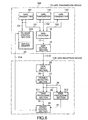
- Fig. 6 is a block diagram for schematically showing a
constitution of a data transfer apparatus according to a second
embodiment of the present invention.
-
Detailed Description of the Preferred Embodiments:
-
Referring to Figs. 1 through 5, description will proceed to
a data transfer apparatus according to a first embodiment of the
present invention. Fig. 1 schematically shows a constitution of the
data transfer apparatus according to the first embodiment of the
present invention. As illustrated in Fig. 1, the data transfer
apparatus 10 comprises a data transmission device 11 which carries
out transmission of data, a data reception device 12 which carries
out reception of data, and a data transfer means 13 which is located
between the data transmission device 11 and the data reception
device 12 as an interface having comparatively low reliability. The
data transmission device 11 comprises first, second, third data
transmitters 141, 142, 143 which output output data 151, 152, 158,
respectively, a data selector 16 which selects the output data 151,
152, 153 of the first, second, third data transmitters 141, 142, 143 to
be outputted as selected data 17, and a data output section 18 to
which the selected data 17 are inputted and which outputs the
selected data 17 to the data transfer means 13. In addition, the
data transmission device 11 further comprises a re-issue control
section 22 to which a re-issue instruction 21 is inputted and which
controls the re-issue of transferred data 19, when the transferred
data 19 sent to the data reception device 12 have an error and the
re-issue instruction 21 is returned from the data reception device 12
to the data transmission device 11. Based on the re-issue
instruction 21, the re-issue control section 22 sends a re-issue
requirement signal 23 to a corresponding one of the first, second,
third data transmitters 141, 142, 143.
-
Herein, data storing means are composed of the first,
second, third data transmitters 141, 142, 143, respectively. The
data storing means are for use in storing data of which transmission
timing must not be influenced by delay of transmission timing of the
other data at least with the data being stored separately to each
other. In this embodiment, the first data transmitter 141 receives
and stores data written in a first memory (not shown) located at the
side of the data reception device 12 one by one. Further, the second
data transmitter 142 receives and stores data written in a second
memory (not shown) located similarly at the side of the data
reception device 12 one by one. Furthermore, the third data
transmitter 143 receives and stores data sent to an I/O device (not
shown) located similarly at the side of the data reception device 12
one by one.
-
On the other hand, the data reception device 12 comprises
a data input section 25 to which the transferred data 19 sent to the
data transfer means 13 from the data output section 18 is inputted.
An output data 26 from the data input section 25 is inputted to a
trouble detecting section 27. In the trouble detecting section 27, it
is detected whether or not the output data 26 has a trouble. With
respect to the data sent to the trouble detecting section 27 by one
clock, the trouble detecting section 27 judges, by a clock, whether or
not the data has a trouble. Further, as regards data for which a
correctable trouble, such as one bit error is generated, the trouble
detecting section 27 corrects the data. On the other hand, in a case
that a trouble is uncorrectable by errors being generated over a
plurality of bits at the same time, the trouble detecting section 27
outputs data indicating that.
-
At the output side of the trouble detecting section 27, first
and second data processing sections 311 and 312 which divide the
transferred data are located. In this embodiment, data transferred
to the above-mentioned first and second memories are stored in the
first data processing section 311 while data transferred to the
above-mentioned I/O device are stored in the second data processing
section 312. Alternatively, three data processing sections 311 can
be, of course, prepared in correspondence with the first, second,
third data transmitters 141, 142, 143, respectively, although the
three data processing sections 311 are not shown in Fig. 1. In this
case, it is enough that the transferred data are simply divided one to
one.
-
As illustrated in Fig. 1, general cancel information 32, 33
are outputted from the first, the second data processing sections 311,
312 respectively. The general cancel information 32, 33 are
supplied to an error judging section 34 which carries out judgment
of errors, respectively. Herein, "general cancel" in this
specification is a general re-try of access. The "general cancel" is
hereunder explained using an example of a general circuit. For
example, in conducting a memory access, when a requirement for
reading data from the memory is generated during writing
operation of the other data to the memory, a problem of concurrence
is inevitably caused to occur. In such a case, a memory access for
reading the data is cancelled and then tried again. Furthermore,
in conducting a memory access, under the circumstances that a
buffer (not shown) for waiting access is filled, it is also necessary
that the access is cancelled and then tried again. Namely,
information for indicating a cancellation of access thus generally
conducted are the general cancel information 32, 33 in this
specification. The general cancel information 32, 33 include data
effectivity information 29 and ID of the data transmitters 141
through 143 as information of transaction thereof.
-
A trouble detecting information 35 obtained by the
detection of the trouble detecting section 27 is inputted to an
information round robin section 86. An error information 37
outputted from the information round robin section 36 is inputted to
the error judging section 34. The information round robin section
36 takes the trouble detecting information 35 around, when an
uncorrectable trouble is detected. The error information 37
outputted from the information round robin section 36 and the
general cancel information 32, 33 are inputted to the error judging
section 34. The error judging section 34 thereby issues a re-issue
instruction 21 for conducting re-issue of data to the data
transmission device 11 under a predetermined condition, as will
later be described.
-
Thus, in the data transfer apparatus 10 in this
embodiment, three data transmitters composed of the first, second,
third data transmitters 141, 142, 143 are used. These data
transmitters 141, 142, 143 are capable of time-division data
transmission with one unit of data transferred by a plurality of
clocks being a minimum unit. Herein, the data are collected per
each kind in which a guarantee of order of transmission is required.
For example, as regards the data sent from the first data
transmitter 141, the order of transmission is guaranteed between
data outputted from the first data transmitter 141. However, the
order of transmission of the data sent from the first data
transmitter 141 is not guaranteed with respect to data outputted
from the second or the third data transmitter 142 or 143.
-
The first, second, third data transmitters 141, 142, 143
are composed of FIFO (First In First Out) buffers, respectively so as
to guarantee the order of transmission. The data selector 16 is
composed of a circuit called as a selector, and so on which select data
by a method, such as round robin scheduling, and the like. Since
such a circuit is well known to those skilled in the art, description
about a detailed constitution of the circuit is herein omitted. The
data output section 18 is composed of a register (not shown) which
holds a transferred data in time-division transmission of the data by
one unit. The data input section 25 is also composed of a register
(not shown), which is located in view of delay of data transfer, and
the like. Since the constitutions of these registers are not related
to the present invention directly, description about detailed
constitutions of the registers is herein omitted. The trouble
detecting section 27 has an ECC (Error Correcting Code) control
circuit (not shown) and detects both a correctable trouble and an
uncorrectable trouble. In a case that the correctable trouble is
detected, the trouble detecting section 27 conducts correction of the
data, as described before. On the contrary, in a case that the
uncorrectable trouble is detected, the trouble detecting section 27
reports the fact that the uncorrectable trouble is detected. Since
this circuit is also well known to those skilled in the art, description
about a detailed constitution of the circuit is herein omitted.
-
Fig. 2 shows a characterizing portion of the data reception
device 12 of the data transfer apparatus according to this
embodiment. In Fig. 2, concretely illustrated is a constitution of
the information round robin section 36 to which the trouble
detecting information 35 is inputted as an output side of the trouble
detecting section 27 to which the output data 26 is inputted. In Fig.
2, also concretely illustrated is a constitution of the first data
processing section 311 to which a transferred data 28 is inputted.
The second data processing section 812 has a constitution of a
circuit similar to that of the first data processing section 311. As a
result, illustration of the second data processing section 312 is
omitted.
-
The information round robin section 36 comprises first,
second, and third registers 41, 42, and 43 as a serial circuit to which
the trouble detecting information 35 is inputted one by one. An
output data 44 of the first register 41 is inputted not only to the
second register 42 but also to the error judging section 34. An
output data 45 of the second register 42 is inputted not only to the
third register 43 but also to the error judging section 34. An
output data 46 of the third register 43 is inputted to the error
judging section 34. Namely, the three output data 44, 45, and 46
are inputted to the error judging section 34 in parallel.
-
On the other hand, the first data processing section 311
comprises a transferred data processing portion 47, a data
effectivity information processing portion 48, and a data processor
49. The transferred data processing portion 47 comprises fourth,
fifth, and sixth registers 51, 52, and 53 as a serial circuit to which a
transferred data 281 is inputted one by one. An output data 54 of
the fourth register 51 is inputted not only to the fifth register 52 but
also to the data processor 49. An output data 55 of the fifth
register 52 is inputted not only to the sixth register 53 but also to
the data processor 49. An output data 66 of the sixth register 53 is
inputted to the data processor 49.
-
The data effectivity information processing portion 48
comprises seventh, eighth, and ninth registers 61, 62, and 63 as a
serial circuit to which a data effectivity information 29 is inputted
one by one. Herein, the data effectivity information 29 is composed
of a part of the transferred data 281. An output data 64 of the
seventh register 61 is inputted not only to the eighth register 62 but
also to the data processor 49. An output data 65 of the eighth
register 62 is inputted not only to the ninth register 63 but also to
the data processor 49. An output data 66 of the ninth register 63 is
inputted to the data processor 49. Namely, the six output data 54,
55, 56, 64, 65, and 66 are inputted to the data processor 49 in
parallel. This is on the assumption that a plurality of data
selectors 16 illustrated in Fig. 1 and a plurality of circuit portions
previous to the data selectors 16 exist, and that the transferred data
19 outputted from a plurality of data selectors 16 are subjected to a
pipeline processing. The output data 66 of the ninth register 63 is
also inputted to the error judging section 34 in addition to the data
processor 49.
-
The general cancel information 32 outputted from the
data processor 49 is inputted to the error judging section 34.
Annulment information 69 from the error judging section 34 is
inputted to the data processor 49. Herein, the annulment
information 69 is such information for indicating an annulment of
data that come to be, by re-sending, overlapping with a previously
sent data among data sent from the data transmission device 11
illustrated in Fig. 1.
-
In the data transfer apparatus 10 of this embodiment
having a constitution thus mentioned, respective data of one unit
sent from the data transmission device 11 to the data reception
device 12 is, as data of three clocks of basic clocks outputted from a
clock generator (not shown), transmitted to the data transfer means
13 per each data of one clock one by one. The first data processing
section 311 is capable of carrying out processing one by one from the
time that a head data of three-divided transferred data 281 reaches.
In this point, the second data processing section 312 illustrated in
Fig. 1 is similar to the first data processing section 311. In that
case, the second data processing section 312 carries out processing
one by one from the time that a head data of three-divided
transferred data 28 reaches.
-
The trouble detecting information 35, which is outputted
from the trouble detecting section 27 and which is inputted to the
information round robin section 36, comprises (1) whether or not
uncorrectable trouble exists, (2) an identification number indicating
which the output data is outputted from, the first, the second, or the
third data transmitter 141, 142, or 143, and (3) a read pointer as a
reading position of any one of the first, the second, and the third
data transmitters 141, 142, and 143 in the time of re-sending.
When the uncorrectable trouble is generated, the error judging
section 34 to which the error information 37 is inputted returns, as
the re-issue instruction 21, an effectivity flag, the identification
number of the first, the second, or the third data transmitter 141,
142, or 143 of round robin information, and the read pointer of the
corresponding the first, the second, or the third data transmitter
141, 142, or 143. The error judging section 34 thereby requires the
re-issue from the corresponding the first, the second, or the third
data transmitter 141, 142, or 143.
-
In the interim, even if a status of the trouble detecting
information 35 indicates that the uncorrectable trouble does not
exist, the error judging section 84 issues the re-issue instruction 21
in a case that the general cancel information 32 (33) detected by the
first data processing section 311 (second data processing section
312) is active. With respect to one of the first, the second, and the
third data transmitters 141, 142, and 143 corresponding to the
identification number of the first, the second, or the third data
transmitter 141, 142, or 143 of round robin information, the re-issue
control section 22 sets the read pointer of the round robin
information onto the read pointer of the above-mentioned FIFO
buffer. It thereby becomes possible to conduct the re-issue of the
output data 151, 152, or 153 from a portion that re-sending is
required. In a case that the re-issue of the output data 151, 152, or
153 is conducted, following transferred data issued by slip are
annulled in the first (the second) data processing section 311 (312)
by transmitting the annulment information 69 to the first (the
second) data processing section 311 (312). In the error judging
section 34, a decrement counter is located with being corresponding
to the identification number of the first, the second, or the third
data transmitter 141, 142, or 143 for which the re-issue instruction
21 becomes active. The decrement counter is decremented by fixed
numbers of clocks to become "0". When the decrement counter
shows values other than "0", the annulment information 69
corresponding to the data transmitter of an issue source becomes
active. Accordingly, the above-mentioned processing is carried out.
-
Figs. 3 through 5 show data transfer operations of the
data transfer apparatus according to this embodiment with time
base being divided into three. Besides, Figs. 3, 4, and 5 are
partially overlapping with each other. In Figs. 3 through 5, (a)
shows basic clocks 71 used in the data transfer apparatus 10. Time
T1, T2,.... depicted above the basic clocks 71 show respective clock
periods.
-
In Figs. 3 through 5, (b) shows definers 72. The definers
72 show mediation timing, when the data selector 16 in the data
transmission device 11 selects the output data 151, 152, or 153
outputted from the first, the second, or the third data transmitter
141, 142, or 143. In this embodiment, the definers 72 become
active once every three clocks of the basic clocks 71. In the
example being illustrated, the definers 72 become active at the time
T0, T3, T6, ...., respectively.
-
In Figs. 3 through 5, (c) shows an example of a
constitution of the transferred data 19 transferred by the data
output section 18 illustrated in Fig. 1. Herein, a transferred data A
shows a data transmitted by the first data transmitter 141
illustrated in Fig. 1 while a transferred data B shows a data
transmitted by the second data transmitter 142 illustrated in Fig. 1.
It is assumed that a data transmitted by the third data transmitter
143 illustrated in Fig. 1 does not exist within the time period
depicted in Figs. 3 through 5, for the brevity of explanation.
Besides, numbers "00" to "02" added to the respective transferred
data A, B show an order of the transferred data of one unit as the
precedent first half portion. On the other hand, the other numbers
"10" to "12" show an order of the transferred data of one unit as the
second half portion following to the precedent first half portion.
-
Symbols "D" added following to the two-digit numbers
"00" and the like do not have special meanings in this specification.
The symbols "D" are added in order to prevent the numbers "00" and
the like from being confused with the other two-digit numbers
showing the other parts of circuits in this specification. On the
contrary, in Figs. 3 through 5, depicted are such data in which
symbols "S" or symbols "E" are added following to the two-digit
numbers. The data to which the symbols "S" are added show
trouble detecting information for indicating that the uncorrectable
troubles do not exist. On the contrary, the data to which the
symbols "E" are added show trouble detecting information for
indicating that the uncorrectable troubles exist.
-
In the interim, it is assumed that transferred data A00D,
A01D, A02D as the transferred data of the precedent one unit and
transferred data A10D, A11D, A12D as the transferred data
following thereto are stored in this order in the FIFO buffer of the
first data transmitter 141. Further, it is also assumed that
transferred data B00D, B01D, B02D as the transferred data are
stored in the FIFO buffer of the second data transmitter 142.
Moreover, it is also assumed that, such an interface that the
transferred data 19 outputted from the data output section 18 is
received by the data input section 25 after four clocks periods of the
basic clocks 71 is used as the data transfer means 13 in this
embodiment.
-
In Figs. 3 through 5, (d) shows a receiving condition of the
data input section 25 in the data reception device 12. In the same
figures, (e), (f), (g) show storing conditions of the seventh, the eighth,
the ninth registers 61, 62, 63 illustrated in Fig. 2, respectively.
Further, in the same figures, (h), (i), (j) show storing conditions of
the fourth, the fifth, the sixth registers 51, 52, 53 illustrated in Fig.
2, respectively. Furthermore, in the same figures, (k), (l), (m) show
storing conditions of the first, the second, the third registers 41, 42,
43 illustrated in Fig. 2, respectively.
-
On the assumption thus mentioned, it is also assumed
that at first, only one unit (of three clocks of the basic clocks 71) of
the output data 151 of the first data transmitter 141 is selected by
the data selector 16 at the time T0 and decided as a selected data 17
transferred to the data output section 18.
-
Accordingly, at the next time T1, a first transferred data
A00D among the data of one unit is transmitted from the data
output section 18 to the data reception device 12 as the transferred
data 19.
-
Further, at the next time T2, a second transferred data
A01D among the data of one unit is transmitted from the data
output section 18 to the data reception device 12 as the transferred
data 19.
-
At the next time T3, the definers 72 become active, and
then next one unit (of three clocks of the basic clocks 71) of the
output data 152 of the second data transmitter 142 is selected by
the data selector 16 and decided as a selected data 17 transferred to
the data output section 18. At this time, a third transferred data
A02D among the data of one unit which has already been selected
from the first data transmitter 141 is transmitted from the data
output section 18 to the data reception device 12 as the transferred
data 19.
-
At the next time T4, a first transferred data B00D among
the data of one unit outputted from the second data transmitter 142
is transmitted from the data output section 18 to the data reception
device 12 as the transferred data 19.
-
Further, at the next time T5, a second transferred data
B01D among the data of one unit is transmitted from the data
output section 18 to the data reception device 12 as the transferred
data 19. At this time, as illustrated in Fig. 3 (d), the first
transferred data A00D transmitted at the time T1 from the data
output section 18 is received by the data input section 25 of the data
reception device 12 with a delay of four clocks periods of the basic
clocks 71.
-
At the next time T6, the definers 72 become active.
However, as described before, data transmitted from the third data
transmitter 143 shown in Fig. 1 do not exist at this time. As a
result, the output data 151 of the first data transmitter 141 is
selected by the data selector 16 again. Thereby, a selected data 17
of one unit (of three clocks of the basic clocks 71) inputted to the
data output section 18 is decided. At the time T6, a third
transferred data B02D among the data of one unit is transmitted
from the data output section 18 to the data reception device 12 as
the transferred data 19. Further, at this time T6, the second
transferred data A01D is received by the data input section 25 of the
data reception device 12.
-
In the interim, at the above-described time T6, the data
effectivity information 29 is received by the seventh register 61. At
this time, the first transferred data A00D is received by the fourth
register 51. Also at this time, a trouble detecting information
A00E for the first transferred data A00D is inputted to the first
register 41 in the information round robin section 36 to which the
trouble detecting information 35 is inputted. Namely, in this case,
it is detected by the trouble detecting section 27 that the first
transferred data A00D has the uncorrectable trouble. In this case,
the data transfer apparatus 10 has the status that the
uncorrectable trouble exists. Thus, the status that the
uncorrectable trouble exists is shown by converting the symbol "D"
indicated at an end of transferred data into the symbol "E" in this
specification.
-
Further, at the next time T7, a first transferred data A10D
among the data of following one unit is transmitted from the data
output section 18 to the data reception device 12 as the transferred
data 19. At this time, the third transferred data A02D is received
by the data input section 25. In addition, the second transferred
data A01D is received by the fourth register 51 while the first
transferred data A00D is received by the fifth register 52. Also at
this time, a trouble detecting information A01S for the second
transferred data A01D is received by the first register 41 in the
information round robin section 36 to which the trouble detecting
information 35 is inputted. Namely, in this case, it is not detected
by the trouble detecting section 27 that the second transferred data
A01D has the uncorrectable trouble. In this case, the data transfer
apparatus 10 has the status that the uncorrectable trouble does not
exist. Thus, the status that the uncorrectable trouble does not
exist is shown by converting the symbol "D" indicated at an end of
transferred data into the symbol "S" in this specification. At this
time T7, a trouble detecting information A00E outputted from the
first register 41 for the first transferred data A00D is received by
the second register 42.
-
Further, at the next time T8, a second transferred data
A11D among the data of following one unit is transmitted from the
data output section 18 to the data reception device 12 as the
transferred data 19. At this time, the first transferred data B00D
is received by the data input section 25. In addition, the third
transferred data A02D is received by the fourth register 51 while
the second transferred data A01D outputted from the fourth
register 51 is received by the fifth register 52. Further, the first
transferred data A00D outputted from the fifth register 52 is
received by the sixth register 53.
-
Also at this time, a trouble detecting information A02S for
the third transferred data A02D is received by the first register 41
in the information round robin section 36 to which the trouble
detecting information 35 is inputted. Namely, in this case, it is not
detected by the trouble detecting section 27 that the third
transferred data A02D has the uncorrectable trouble. In this case,
the data transfer apparatus 10 has the status that the
uncorrectable trouble does not exist. At this time T8, a trouble
detecting information A01S outputted from the first register 41 for
the second transferred data A01D is received by the second register
42. Also at this time, a trouble detecting information A00E
outputted from the second register 42 is received by the third
register 43. At the time T8, the ninth register 63 receives the data
effectivity information 29 to become active. The error judging
section 34 is adjusted to output error information 87 on a condition
that any one of the first, the second, and the third registers 41, 42,
and 43 stores a status of existence of the uncorrectable trouble. On
the condition that the error information 37 is outputted and that the
ninth register 63 becomes active, the error judging section 34
renders the re-issue instruction 21 to be active, as illustrated in Fig.
4(n).
-
Further, at the next time T9, based on the re-issue
instruction 21 having become active, the re-issue requirement
signal 23 is issued from the re-issue control section 22 to the first
data transmitter 141 in the data transmission device 11, as
illustrated in Fig. 4 (o). Based on this, the re-issue output data 151
from the first data transmitter 141 is indicated by a read pointer
and selected by the data selector 16. The selected data 17 to the
data output section 18 is thereby decided. At this time, a
previously selected third transferred data A12D is transmitted from
the data output section 18. At this time, the second transferred
data B01D is received by the data input section 25. Further, at
this time, the data effectivity information 29 from the trouble
detecting section 27 is received by the seventh register 61.
-
Further, the first transferred data B00D is received by the
fourth register 51. The third transferred data A02D outputted
from the fourth register 51 is received by the fifth register 52. The
second transferred data A01D outputted from the fifth register 52 is
received by the sixth register 53. Further, also at this time, it is
assumed that a trouble detecting information B00S for the first
transferred data B00D is received by the first register 41. Namely,
in this case, it is not detected by the trouble detecting section 27
that the first transferred data B00D has the uncorrectable trouble.
In this case, the data transfer apparatus 10 has the status that the
uncorrectable trouble does not exist. At this time T9, a trouble
detecting information A02S outputted from the first register 41 is
received by the second register 42. A trouble detecting information
A01S outputted from the second register 42 is received by the third
register 43. Also at this time, the re-issue instruction 21 from the
error judging section 34 is received by the re-issue control section 22.
By the re-issue instruction 21, the annulment information 69
outputted from the error judging section 34 becomes active, as
illustrated in Fig. 4 (p).
-
When a re-sending is conducted for the output data 151
outputted from the first data transmitter 141, an interval that the
annulment information 69 is kept active is equal to six clocks of the
basic clocks 71. The error judging section 34 memorizes a time for
which the annulment information 69 is kept active by the numbers
of clocks of the basic clocks 71 as regards the first, the second, the
third data transmitters 141, 142, 143, respectively. In this
example, the annulment information 69 is kept active in order that
an information of generation of cancellation for the first half
transferred data of the output data 151 outputted from the first
data transmitter 141 may be held until a timing the second half of
the output data 151 or the numbers of clocks of the basic clocks 71 of
slip (the numbers of transaction) reaches.
-
Further, at the next time T10, based on the re-issue
instruction 21, the first transferred data A00D by the re-sending is
transmitted from the data output section 18. At this time, the
third transferred data B02D is received by the data input section 25.
Further, an output data outputted from the seventh register 61 is
received by the eighth register 62. The second transferred data
B01D is received by the fourth register 51. The first outputted
data B00D outputted from the fourth register 51 is received by the
fifth register 52. The third outputted data A02D outputted from
the fifth register 52 is received by the sixth register 53. A trouble
detecting information B01S for the second transferred data B01D is
received by the first register 41. In this case, it is not detected by
the trouble detecting section 27 that the second transferred data
B01D has the uncorrectable trouble. In this case, the data transfer
apparatus 10 has the status that the uncorrectable trouble does not
exist. The first outputted data B00S outputted from the first
register 41 is received by the second register 42. The third
outputted data A02S outputted from the second register 42 is
received by the third register 43. The annulment information 69 is
kept active.
-
Further, at the next time T11, the second transferred data
A01D by the re-sending is transmitted from the data output section
18. At this time, the first transferred data A10D is received by the
data input section 25. Further, an output data outputted from the
eighth register 62 is received by the ninth register 63. The third
transferred data B02D is received by the fourth register 51. The
outputted data B01D outputted from the fourth register 51 is
received by the fifth register 52. The first outputted data B00D
outputted from the fifth register 52 is received by the sixth register
53. A trouble detecting information B02S for the third transferred
data B02D is received by the first register 41. In this case, it is not
detected by the trouble detecting section 27 that the third
transferred data B02D has the uncorrectable trouble. In this case,
the data transfer apparatus 10 has the status that the
uncorrectable trouble does not exist. The outputted data B01S
outputted from the first register 41 is received by the second
register 42. The outputted data B00S outputted from the second
register 42 is received by the third register 43. The annulment
information 69 is kept active. At this time, although the ninth
register 63 is active, any one of the first, the second, and the third
registers 41, 42, and 43 in the information round robin section 36
does not have the status that the uncorrectable trouble exists. As a
result, at the time T11, the re-issue instruction 21 does not become
active. Accordingly, as regards the data B00D, B01D, and B02D
transferred from the second data transmitter 142, processing is
normally completed without conducting the re-sending processing.
-
Further, at the next time T12, the output data 151 from
the first data transmitter 141 is selected by the data selector 16.
The selected data 17 to the data output section 18 is thereby decided.
In addition, the third transferred data A02D is transmitted from the
data output section 18. At this time, the second transferred data
A11D is received by the data input section 25. Further, the data
effectivity information 29 is received by the seventh register 61.
The first transferred data A10D is received by the fourth register 51.
The output data B02D outputted from the fourth register 51 is
received by the fifth register 52. The output data B01D outputted
from the fifth register 52 is received by the sixth register 53. A
trouble detecting information A10S for the first transferred data
A10D is received by the first register 41. In this case, it is not
detected by the trouble detecting section 27 that the first
transferred data A10D has the uncorrectable trouble. In this case,
the data transfer apparatus 10 has the status that the
uncorrectable trouble does not exist. The output data B02S
outputted from the first register 41 is received by the second
register 42. The output data B01S outputted from the second
register 42 is received by the third register 43. The annulment
information 69 is kept active.
-
Further, at the next time T13, the first transferred data
A10D as a following transmitted data is transmitted from the data
output section 18. At this time, the third transferred data A12D is
received by the data input section 25. Further, an output data
outputted from the seventh register 61 is received by the eighth
register 62. The second transferred data A11D is received by the
fourth register 51. The output data A10D outputted from the
fourth register 51 is received by the fifth register 62. The output
data B02D outputted from the fifth register 52 is received by the
sixth register 53. A trouble detecting information A11S for the
second transferred data A11D is received by the first register 41.
In this case, it is not detected by the trouble detecting section 27
that the second transferred data A11D has the uncorrectable
trouble. In this case, the data transfer apparatus 10 has the status
that the uncorrectable trouble does not exist. The output data
A10S outputted from the first register 41 is received by the second
register 42. The output data B02S outputted from the second
register 42 is received by the third register 43. The annulment
information 69 is kept active.
-
Further, at the next time T14, the second transferred data
A11D is transmitted from the data output section 18. At this time,
the first transferred data A00D is received by the data input section
25. Further, an output data outputted from the eighth register 62
is received by the ninth register 63. The third transferred data
A12D is received by the fourth register 51. The output data A11D
outputted from the fourth register 51 is received by the fifth register
52. The output data A10D outputted from the fifth register 52 is
received by the sixth register 53. A trouble detecting information
A12S for the third transferred data A12D is received by the first
register 41. In this case, it is not detected by the trouble detecting
section 27 that the third transferred data A12D has the
uncorrectable trouble. In this case, the data transfer apparatus 10
has the status that the uncorrectable trouble does not exist. The
output data A11S outputted from the first register 41 is received by
the second register 42. The output data A10S outputted from the
second register 42 is received by the third register 43. The
annulment information 69 is kept active. The annulment
information 69 makes the data effectivity information of the ninth
register 63 be invalid. Namely, the transferred data A10D, A11D,
and A12D are completed without conducting processing. On the
other hand, a previous processing may be conducted, when the
seventh register 61 and the eighth register 62 are active. However,
when the ninth register 63 of the last stage is active, all processing
are rendered to be invalid.
-
Further, at the next time T15, the third transferred data
A12D is transmitted from the data output section 18. At this time,
the second transferred data A01D is received by the data input
section 25. Further, the data effectivity information 29 is received
by the seventh register 61. The first transferred data A00D is
received by the fourth regieter 51. The third output data A12D
outputted from the fourth register 51 is received by the fifth register
52. The second output data A11D outputted from the fifth register
52 is received by the sixth register 53. A trouble detecting
information A00S for the first transferred data A00D is received by
the first register 41. In this case, it is not detected by the trouble
detecting section 27 that the first transferred data A00D has the
uncorrectable trouble. In this case, the data transfer apparatus 10
has the status that the uncorrectable trouble does not exist. The
output data A12S outputted from the first register 41 is received by
the second register 42. The output data A11S outputted from the
second register 42 is received by the third register 43. The
annulment information 69 inputted to the data processor 49
becomes inactive from this time.
-
Further, at the next time T16, the third transferred data
A02D is received by the data input section 25. Further, an output
data outputted from the seventh register 61 is received by the
eighth register 62. The second transferred data A01D is received
by the fourth register 51. The first output data A00D outputted
from the fourth register 51 is received by the fifth register 52. The
third output data A12D outputted from the fifth register 52 is
received by the sixth register 53. A trouble detecting information
A01S for the second transferred data A01D is received by the first
register 41. In this case, it is not detected by the trouble detecting
section 27 that the second transferred data A01D has the
uncorrectable trouble. In this case, the data transfer apparatus 10
has the status that the uncorrectable trouble does not exist. The
output data A00S outputted from the first register 41 is received by
the second register 42. The output data A12S outputted from the
second register 42 is received by the third register 43.
-
Further, at the next time T17, the first transferred data
A10D is received by the data input section 25. Further, an output
data outputted from the eighth register 62 is received by the ninth
register 63. The third transferred data A02D is received by the
fourth register 51. The second output data A01D outputted from
the fourth register 51 is received by the fifth register 52. The first
output data A00D outputted from the fifth register 52 is received by
the sixth register 53. A trouble detecting information A02S for the
third transferred data A02D is received by the first register 41. In
this case, it is not detected by the trouble detecting section 27 that
the third transferred data A02D has the uncorrectable trouble. In
this case, the data transfer apparatus 10 has the status that the
uncorrectable trouble does not exist. The output data A01S
outputted from the first register 41 is received by the second
register 42. The output data A00S outputted from the second
register 42 is received by the third register 43. At this time,
although the ninth register 63 is active, any one of the first, the
second, and the third registers 41, 42, and 43 in the information
round robin section 36 does not have the status that the
uncorrectable trouble exists. As a result, at the time T17, the
re-issue instruction 21 does not become active. Accordingly, as
regards the data A00D, A01D, and A02D transferred from the first
data transmitter 141, processing is normally completed.
-
Following to the above, as regards following data A10D,
A11D, and A12D transferred from the first data transmitter 141,
processing is conducted by the steps similar to the above.
-
Thus, in the example described above, among the data
A00D, A01D, and A02D transferred from the first data transmitter
141, the uncorrectable trouble is detected in the first transferred
data A00D. Consequently, processing of re-sending is conducted
for the first transferred data A00D. However, following
transferred data B00D, B01D, and B02D transferred from the
second data transmitter 142 are not at all influenced by this
processing of re-sending.
-
As described above, even if the uncorrectable trouble is
generated in the data, the data is re-issued from the corresponding
data transmitter, similarly to the general cancellation. As a result,
an operation of the data transfer can be conducted without
influencing following transferred data issued from the other data
transmitters.
-
Namely, there is no time that influences following transfer
of data and that is caused by processing of re-sending, even when
the uncorrectable trouble is generated. As a result, a performance
as a whole of the system is greatly improved. In the example
described in this embodiment, among the data A00D, A01D, and
A02D transferred from the first data transmitter 141, the
uncorrectable trouble is detected in the first transferred data A00D.
Consequently, processing of re-sending is conducted for the first
transferred data A00D. However, following transferred data B00D,
B01D, and B02D transferred from the second data transmitter 142
are not at all influenced by this processing of re-sending. Besides,
as regards transferred data A10D, A11D, and A12D issued by slip
before the re-issue from the first data transmitter 141, it is
necessary that an order of transfer is guaranteed between the
transferred data A10D, A11D, A12D and the data A00D, A01D,
A02D. In view of this, the data transfer apparatus 10 comprises
means for re-sending those data A10D, A11D, and A12D and
annulling the re-sent data A10D, A11D, and A12D thereafter. In
this embodiment, without adding new functions especially for the
uncorrectable trouble, coexistence with the general cancellation
function is available. It is not at all necessary that hardware for
exclusive use of re-sending is prepared. Thereby, reduction of cost
can be achieved in this embodiment.
-
On the other hand, in a conventional technique, a
re-sending instruction is issued to a data transmission device, after
a trouble detecting result is obtained in a data reception device. As
a result, a flight time of an interface between the data transmission
device and the data reception device inevitably appears in a
performance of a data transfer apparatus. Further, since following
data must wait for their transfer during re-sending, such following
data for which an order of transfer does not need to be considered at
all is also influenced by the re-sending. Further, in the
countermeasure that a re-sending buffer is prepared in a data
transmission device and that, every time data is transmitted, the
data is stored in the re-sending buffer, the data is re-issued from the
re-sending buffer, when a trouble is detected. However, in this
countermeasure, quantity of hardware is largely increased. In
addition, it becomes necessary to conduct mediation, or the like
between output data from the re-sending buffer and general data.
Implement thereof is also complicated. However, an advantageous
effect that an efficient system can be constituted with a compact
hardware in this embodiment.
-
In the first embodiment thus described above, the data
transfer apparatus 10 has the information round robin section 36,
so that the trouble detecting information 35 obtained by detection of
the trouble detecting section 27 is taken around. However, the
information round robin section 36 takes the identification numbers
of the data transmitters 141 to 143, and read pointers of the data
transmitters 141 to 143 around. As a result, when the
uncorrectable trouble exists in these, a data transmitter 141, 142, or
143 of a transmission source cannot be identified. Therefore, the
embodiment has a little possibility that data transfer incapable of
being relieved is generated. Namely, in a case that an
uncorrectable trouble exists in the first transferred data, the data
transfer apparatus brings about a system down. Such a problem
can be solved by providing a circuit corresponding to the
information round robin section 36 in the first embodiment at the
side of the data transmission device 11. This will be hereunder
described as a second embodiment of the present invention.
-
Fig. 6 schematically shows a constitution of a data
transfer apparatus according to a second embodiment of the present
invention. In Fig. 6, portions similar to those of Fig. 1 are
designated by like reference numerals and explanation thereof is
omitted accordingly. In the data transfer apparatus 10A according
to the second embodiment, a re-issue control section 22A in a data
transmission device 11A comprises a buffer memory 81. On the
other hand, a data reception device 12A does not have the
information round robin section 36 (in Fig. 1). A role of the
information round robin section 36 is conducted by the buffer
memory 81.
-
Namely, in the data transfer apparatus 10A according to
the second embodiment, the identification numbers of the data
transmitters 141 to 143 and the read pointers of the data
transmitters 141 to 143 each of which is corresponding to a
transferred data issued from the data transmitter 141, 142, or 143
are registered in the buffer memory 81 of the re-issue control section
22A one by one. When the uncorrectable trouble is generated, a
re-issue instruction 21A having no additional information for the
read pointers of the data transmitters 141 to 143, and the like is
returned from the error judging section 34.
-
The number of clocks of the basic clocks 71 (shown in Fig.
3) until a transferred data reaches the error judging section 34 after
the transferred data is issued from the data output section 18 is a
fixed number. Therefore, in a case that a re-issue instruction 21A
is not generated at the timing for generating the re-issue
instruction 21A, it is decided that the re-issue does not need to be
conducted. Namely, the data transfer apparatus 10A makes the
identification numbers of the data transmitters 141 to 143 and the
read pointers of the data transmitters 141 to 143 both of which are
registered in the buffer memory 81 of the re-issue control section
22A be invalid. At the timing that a data to be transmitted is read
out of any one of the data transmitters 141, 142, and 143, an
identification number of the data transmitter 141, 142, or 143 and
the read pointer of the data transmitter 141, 142, or 143 are written
into the buffer memory 81. Then, in a case that a re-issue
instruction 21A is active at the timing for generating the re-issue
instruction 21A, data indicated by the present read pointer, namely,
the identification number of the data transmitter 141, 142, or 143
and the read pointer of the data transmitter 141, 142, or 143 are
read out. At the same time, these read pointers are incremented.
-
On the other hand, in a case that a re-issue instruction
21A is inactive at the timing for generating the re-issue instruction
21A, only increment of the read pointers is conducted. The
above-described reading operation is not conducted.
-
In the second embodiment illustrated in Fig. 6, with the
structure thus mentioned, a rate of relieving data in the data
transfer means 13 as an interface having low reliability at the time
of generation of a trouble is more improved than that of the data
transfer apparatus 10 of the first embodiment.
-
Besides, in the first and the second embodiments, the data
transfer is conducted in a three-divided manner. However, the
number of division is not restricted to three. The number of
division may be any numbers, as far as the number is a positive
integer. Further, in the first embodiment, a reaching time of the
transferred data 19 from the data transmission device 11 to the data
reception device 12 is equal to four clocks of the basic clocks 71.
However, this is also not restricted to four. The number of the
clocks may be any numbers, as far as the number is a positive
integer.
-
Further, in the first and the second embodiments, the data
transmitter is composed of three data transmitters 141, 142, and
143. However, the number of the data transmitter is not restricted
to three. Further, these data transmitters 141, 142, and 143 are
composed of FIFO memories. The data transmitters 141, 142, and
143 are not restricted to such FIFO memories. For example, a
constitution similar to the FIFO memories may be alternatively
obtained by conducting a control for protecting an order of
transferring data using an arithmetic processing unit, such as a
microprocessor, and the like.
-
Furthermore, in the first and the second embodiments,
two data processing sections composed of the first and the second
data processing sections 311 and 312 are used. However, the data
processing section can, of course, be composed of any numbers of the
data processing sections. Further, the data processing section may
be composed of a memorizing device, and the like for storing data.
-
Further, in the first embodiment, an order of transferring
data is guaranteed in the same data transmitter 141, 142, or 143
among the first to the third data transmitters 141 to 143. This is
not restricted to the above. In such a case that the order of
transferring data is not guaranteed, it is not necessary to re-issue
the data after receiving the re-issue instruction 21 with being
entangled therein by a re-set of an effective flag within the first, the
second and the third data transmitters 141, 142 and 143 as regards
the data having already been issued. In addition, in this case, it is
not necessary to control the annulment information 69 in the error
judging section 34. With the control of the annulment information
69 being unnecessary, traffics between the data transmission device
11 (11A) and the data reception device 12 (12A) can be reduced to be
more efficient.
-
Furthermore, in the first embodiment, data transfer
means 13 as an interface is rendered to have one to one connection
between the data transmission device 11 and the data reception
device 12. A plurality of data transmission devices and a plurality
of data reception devices may be connected to the data transfer
means 13 by using a bus connection, or the like. In a case that a
plurality of data transmission devices are used in a single data
transfer means 13, a data transmitter of a data transmission source
can be identified by taking the numbers of the data transmission
devices of a data transmission source around in addition to the
identification numbers of the data transmitters 141, 142, 143 and
the read pointers of the data transmitters 141, 142, 143.
-
Moreover, in the first embodiment, definers are used for
the mediation timings in the data selector 16. However, it is
alternative that the mediations are conducted at any timings and
acknowledges from the data output section 18 are waited therefor.
Besides, the data output section 18 and the data input section 25
are composed of registers. However, the data output section 18 and
the data input section 25 may be composed of the other circuit
devices, such as buffers, and the like.
-
Moreover, in the first embodiment, while the
uncorrectable troubles are repeated, re-issues of the data are also
repeated. In a case that uncorrectable troubles similar to each
other are detected a plurality of times, a check of the system itself
may be conducted as a disorder or a trouble each incapable of being
restored at the present time. Further, in the first and the second
embodiments, ECC control circuits are used for detecting the
uncorrectable troubles. Any detecting means, such as a parity
check, and the like can also be used.
-
As described above, according to the present invention,
the data transfer apparatus has a plurality of data storing means
for storing data of which transmission timing must not be
influenced by delay of transmission timing of the other data at least
with the data being stored separately to each other, and data
selecting means for selecting data per one unit one by one at
predetermined frequency and order with respect to said a plurality
of data storing means, respectively. In re-sending of data, when the
corresponding data storing means is selected, data to be re-sent is
read out and is transmitted. As a result, with a simple data
processing or a compact circuit device, an efficient data transfer can
be realized without influence of a delay by re-sending of the other
kind of data. Further, since data is re-sent similarly to a general
cancellation, a circuit can be commonly used. It is not at all
necessary that hardware for exclusive use of re-sending is prepared.
Thereby, reduction of cost can be achieved in the data transfer
apparatus.