EP1365481A2 - Card-edge connector and card member - Google Patents
Card-edge connector and card member Download PDFInfo
- Publication number
- EP1365481A2 EP1365481A2 EP03011442A EP03011442A EP1365481A2 EP 1365481 A2 EP1365481 A2 EP 1365481A2 EP 03011442 A EP03011442 A EP 03011442A EP 03011442 A EP03011442 A EP 03011442A EP 1365481 A2 EP1365481 A2 EP 1365481A2
- Authority
- EP
- European Patent Office
- Prior art keywords
- card
- connector
- edge
- circuit board
- edge electrodes
- Prior art date
- Legal status (The legal status is an assumption and is not a legal conclusion. Google has not performed a legal analysis and makes no representation as to the accuracy of the status listed.)
- Granted
Links
- 238000009413 insulation Methods 0.000 claims abstract description 43
- 239000002184 metal Substances 0.000 claims description 13
- 229910052751 metal Inorganic materials 0.000 claims description 13
- 238000003780 insertion Methods 0.000 claims description 11
- 230000037431 insertion Effects 0.000 claims description 11
- 230000013011 mating Effects 0.000 claims description 3
- 229910000679 solder Inorganic materials 0.000 description 10
- 239000012535 impurity Substances 0.000 description 7
- 230000002950 deficient Effects 0.000 description 5
- RYGMFSIKBFXOCR-UHFFFAOYSA-N Copper Chemical compound [Cu] RYGMFSIKBFXOCR-UHFFFAOYSA-N 0.000 description 2
- 229920000106 Liquid crystal polymer Polymers 0.000 description 2
- 239000004977 Liquid-crystal polymers (LCPs) Substances 0.000 description 2
- PXHVJJICTQNCMI-UHFFFAOYSA-N Nickel Chemical compound [Ni] PXHVJJICTQNCMI-UHFFFAOYSA-N 0.000 description 2
- 238000003491 array Methods 0.000 description 2
- 229910052802 copper Inorganic materials 0.000 description 2
- 239000010949 copper Substances 0.000 description 2
- 230000008021 deposition Effects 0.000 description 2
- 230000000694 effects Effects 0.000 description 2
- 239000011521 glass Substances 0.000 description 2
- PCHJSUWPFVWCPO-UHFFFAOYSA-N gold Chemical compound [Au] PCHJSUWPFVWCPO-UHFFFAOYSA-N 0.000 description 2
- 239000010931 gold Substances 0.000 description 2
- 229910052737 gold Inorganic materials 0.000 description 2
- 239000012212 insulator Substances 0.000 description 2
- 238000004519 manufacturing process Methods 0.000 description 2
- 238000010079 rubber tapping Methods 0.000 description 2
- 238000005516 engineering process Methods 0.000 description 1
- 239000000463 material Substances 0.000 description 1
- 238000000034 method Methods 0.000 description 1
- 238000012986 modification Methods 0.000 description 1
- 230000004048 modification Effects 0.000 description 1
- 238000000465 moulding Methods 0.000 description 1
- 229910052759 nickel Inorganic materials 0.000 description 1
- 230000003647 oxidation Effects 0.000 description 1
- 238000007254 oxidation reaction Methods 0.000 description 1
- 238000007747 plating Methods 0.000 description 1
- 239000011347 resin Substances 0.000 description 1
- 229920005989 resin Polymers 0.000 description 1
- KKEYFWRCBNTPAC-UHFFFAOYSA-L terephthalate(2-) Chemical compound [O-]C(=O)C1=CC=C(C([O-])=O)C=C1 KKEYFWRCBNTPAC-UHFFFAOYSA-L 0.000 description 1
Images




Classifications
-
- H—ELECTRICITY
- H01—ELECTRIC ELEMENTS
- H01R—ELECTRICALLY-CONDUCTIVE CONNECTIONS; STRUCTURAL ASSOCIATIONS OF A PLURALITY OF MUTUALLY-INSULATED ELECTRICAL CONNECTING ELEMENTS; COUPLING DEVICES; CURRENT COLLECTORS
- H01R12/00—Structural associations of a plurality of mutually-insulated electrical connecting elements, specially adapted for printed circuits, e.g. printed circuit boards [PCB], flat or ribbon cables, or like generally planar structures, e.g. terminal strips, terminal blocks; Coupling devices specially adapted for printed circuits, flat or ribbon cables, or like generally planar structures; Terminals specially adapted for contact with, or insertion into, printed circuits, flat or ribbon cables, or like generally planar structures
- H01R12/70—Coupling devices
- H01R12/71—Coupling devices for rigid printing circuits or like structures
- H01R12/72—Coupling devices for rigid printing circuits or like structures coupling with the edge of the rigid printed circuits or like structures
- H01R12/721—Coupling devices for rigid printing circuits or like structures coupling with the edge of the rigid printed circuits or like structures cooperating directly with the edge of the rigid printed circuits
-
- H—ELECTRICITY
- H01—ELECTRIC ELEMENTS
- H01R—ELECTRICALLY-CONDUCTIVE CONNECTIONS; STRUCTURAL ASSOCIATIONS OF A PLURALITY OF MUTUALLY-INSULATED ELECTRICAL CONNECTING ELEMENTS; COUPLING DEVICES; CURRENT COLLECTORS
- H01R13/00—Details of coupling devices of the kinds covered by groups H01R12/70 or H01R24/00 - H01R33/00
- H01R13/62—Means for facilitating engagement or disengagement of coupling parts or for holding them in engagement
- H01R13/629—Additional means for facilitating engagement or disengagement of coupling parts, e.g. aligning or guiding means, levers, gas pressure electrical locking indicators, manufacturing tolerances
- H01R13/631—Additional means for facilitating engagement or disengagement of coupling parts, e.g. aligning or guiding means, levers, gas pressure electrical locking indicators, manufacturing tolerances for engagement only
-
- H—ELECTRICITY
- H05—ELECTRIC TECHNIQUES NOT OTHERWISE PROVIDED FOR
- H05K—PRINTED CIRCUITS; CASINGS OR CONSTRUCTIONAL DETAILS OF ELECTRIC APPARATUS; MANUFACTURE OF ASSEMBLAGES OF ELECTRICAL COMPONENTS
- H05K1/00—Printed circuits
- H05K1/02—Details
- H05K1/11—Printed elements for providing electric connections to or between printed circuits
- H05K1/117—Pads along the edge of rigid circuit boards, e.g. for pluggable connectors
-
- H—ELECTRICITY
- H05—ELECTRIC TECHNIQUES NOT OTHERWISE PROVIDED FOR
- H05K—PRINTED CIRCUITS; CASINGS OR CONSTRUCTIONAL DETAILS OF ELECTRIC APPARATUS; MANUFACTURE OF ASSEMBLAGES OF ELECTRICAL COMPONENTS
- H05K2201/00—Indexing scheme relating to printed circuits covered by H05K1/00
- H05K2201/10—Details of components or other objects attached to or integrated in a printed circuit board
- H05K2201/10431—Details of mounted components
- H05K2201/10598—Means for fastening a component, a casing or a heat sink whereby a pressure is exerted on the component towards the PCB
Definitions
- the present invention relates to a card-edge connector and a card member for an electronic apparatus and more particularly to a card-edge connector and a card member allowing a minimum of defective contact to occur and allowing a minimum of impurities to deposit on the contact points of contacts.
- a conventional card-edge connector applicable to various electronic apparatuses is generally made up of a card member with a printed circuit board and a connector affixed to a board, which is included in an electronic apparatus.
- the card member includes a circuit board, a plurality of card-edge electrodes arranged on the circuit board, and solder resist surrounding the card-edge electrodes.
- the connector includes a housing for receiving the card member and contacts corresponding one-to-one to the card-edge electrodes.
- the conventional card-edge connector described above is superior in electric characteristic to, e.g., a two-piece connector because the card member, which plays the role of one connector, does not have any contact and is relatively short as a contact.
- the above conventional card-edge connector has the following problems left unsolved.
- the contact points of the contacts are shifted from the card-edge electrodes, failing to establish electrical connection.
- the card-edge electrodes cannot be extended to the edge of the circuit board for production reasons. In this condition, when the card member is inserted into the connector, the contact points of the contacts rub the surface of the circuit board or the solder resist. As a result, impurities are apt to deposit on the contact points of the contacts.
- a card-edge connector of the present invention includes a card member including a circuit board and a plurality of card-edge electrodes arranged on the circuit board.
- a connector is affixed to a stationary board and includes a plurality of contacts corresponding one-to-one to the card-edge electrodes.
- the card member further includes an insulation cover covering an area where the card-edge electrodes are arranged and formed with a plurality of slots via which the card-edge electrodes each are partly exposed to the outside. When the card member is inserted into the connector, the card-edge electrodes and contacts are electrically connected to each other.
- the card-edge connector is made up of a card member 40A and a connector 40B provided on a board, which is affixed to, e.g., an electronic apparatus not shown.
- the card member 40A includes a printed Circuit, not shown, and an electrode portion 40C that adjoins one edge of the card member 40A.
- the electrode portion 40C includes a plurality of card-edge electrodes 42 formed on a circuit board 41. Solder resist 43 surrounds the card-edge electrodes 42.
- the edge of the circuit board 41, adjoining the electrode portion 40C, is formed with a taper 46.
- the card-edge electrodes 42, solder resist 43 and taper 46 are formed on both sides of the circuit board 41.
- the connector 40B on the board side includes a housing 44 for receiving the card member 40A and contacts 45 corresponding one-to-one to the card-edge electrodes 42.
- the housing 44 is formed with guides 44a and 44b for guiding opposite side edges 41a and 41b of the card member 40A when the card member 40A is inserted into the housing 44.
- the guides 44a and 44b guide the side edges 41a and 41b of the card member 40A until the electrode portion 40C has been electrically connected to the connector 40B.
- the contact points of the contacts 45 of the connector 40B get on the card-edge electrodes 42 of the card member 40A to thereby establish electrical connection.
- the conventional card-edge connector 40 described above has the following problems when consideration is given to the current trend toward the dense arrangement of card-edge electrodes, e.g., a distance between card-edge electrodes as small as 1 mm or less, e.g., 0.5 mm.
- the card-edge electrodes 42 and contacts 45 are shifted from each other little by little as a distance from a reference position increases although they may be accurately aligned at the reference position.
- the contacts noticeably shifted from the card-edge electrodes 42 would miss the card-edge electrodes 42 and would thereby bring about defective contact.
- the card-edge electrodes 42 cannot be extended to the edge of the circuit board 41 for production reasons.
- the contact points of the contacts 45 rub the surface of the circuit board 41 or the solder resist 43.
- impurities are apt to deposit on the contact points of the contacts 45.
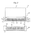
- a card-edge connector embodying the present invention is shown and generally designated by the reference numeral 10.
- the card-edge connector 10 is made up of a card member 10A and a connector 10B provided on a board, which is affixed to, e.g., an electronic apparatus not shown.
- the card member 10A includes a printed circuit, not shown, and an electrode portion 10C that adjoins one edge of the card member 10A.
- An insulation cover 11 is affixed to a circuit board 21 included in the card member 10A.
- a plurality of card-edge electrodes 24 are arranged in the electrode portion 10C of the circuit board 21 and surrounded by solder resist 25.
- the edge of the circuit board 21 is formed with a taper 26.
- the circuit board 21 is formed with holes 22a and 22b for affixing the insulation cover 11 and holes 23a, 23b, 23c and 23d for positioning the insulation cover 11.
- the card-edge electrodes 24 and taper 26 are formed on both sides of the circuit board 21.
- the insulation cover 11 is formed of an insulator and configured to cover the entire area where the card-edge electrodes 24 are arranged.
- the insulation cover 11 is formed with slots 14 corresponding one-to-one to the card-edge electrodes 24.
- the slots 14 each are sized (area) smaller than the corresponding card-edge electrode 24, so that only part of the card-edge electrode 24 is exposed to the outside.
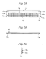
- the insulation cover 11 is formed with holes 12a and 12b that allow the cover 11 to be affixed to the circuit board 21 and lugs 13a and 13b that allow the former to be positioned relative to the latter.
- Opposite side edges 11a and 11b of the insulation cover 11 are so configured as to be parallel to the side edges 21a and 21b of the circuit board 21 when mounted to the circuit board 21 in the direction of insertion.
- the side edges 11a and 11b are provided with higher dimensional accuracy than the side edges 21a and 21b.
- a square metal pad 15 is positioned on the insertion side of each slot 14 at a position where the corresponding contact of the connector 10B slides in the initial stage of insertion.
- the metal pad 15 may be press-fitted or adhered to the cover 11.
- a taper 16 is also formed on the insertion side of the cover and metal pad 15.
- the insulation cover 11 is formed of an insulator except for the metal pads 15.
- the screws 27 may be replaced with tapping screws for directly affixing the insulation covers 11 to the circuit board 21, in which case the hole 12a will be provided with a larger diameter than the hole 12b and a single tapping screw will be positioned on each side of the circuit board 21.
- This scheme makes the washers 28, spring washers 29 and nuts 30 unnecessary.
- the insulation covers 11 may be adhered or otherwise fitted on the circuit board 21. In any case, the configuration of each insulation cover 11 does not have to be varied without regard to the affixing method.
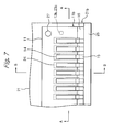
- FIG. 7 shows part of the card member 10A in an enlarged view.
- FIGS. 8A and 8C are sections along lines A-A and B-B of FIG. 7, respectively.
- FIG. 8B is also a section along line A-A of FIG. 7, but showing an inserted condition.
- FIGS. 7, 8A and 8C when each insulation cover 11 is affixed to the circuit board 21, only the card-edge electrodes 24 are exposed to the outside via the slots 14 while the solder resist 25 are the surface of the circuit board 21 hidden below the insulation cover 11.
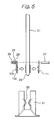
- the connector 10B on the board side includes a housing 31 for receiving the card member 10A and contacts 33 corresponding one-to-one to the card-edge electrodes 24.
- the housing 31 is formed with guides 32a and 32b for guiding opposite side edges 11a and 11b of the insulation cover 11 when the card member 10A is inserted into the housing 31.
- FIGS. 9A and 9B respectively show a condition before the card member 10A is inserted into the connector 10B and a condition after the former has been inserted into the latter.
- the contacts 33 each mate with one of the slots 14.
- the contact point of each contact 33 gets on the corresponding card-edge electrode 24 exposed via the slot 14, establishing electrical connection.
- the contact point of the contact 33 is movable only in the range delimited by the edges of the slot 14 and therefore does not easily slip out of the card-edge electrode 24.
- FIG. 10A shows the leading edge portion of the card member 10A and contacts 33 in the first stage. The contacts 33 then get on the associated metal pads 15 while being guided by the tapers 26 and 16.
- each contact 33 moves on the surface of the associated metal pad 15 while rubbing the metal pad 15.
- a wiping effect occurs on the contact point of the contact 33 and removes oxide or oxide films and impurities from the contact point.
- the contact 33 does not rub the surface of the circuit board 21 or the solder resist 25, obviating the deposition of impurities.
- the contact 33 slips into the slot 14 and contacts the card-edge electrode 24.
- the contact point of the contact 33 is movable only in the range delimited by the edges of the slot 14 and therefore does not easily slip out of the card-edge electrode 24, as stated earlier. Even if the dimensional accuracy of the boundary between nearby card-edge electrodes 24 is relatively low, the card-edge electrode 24 and the contact point of the contact 33 can accurately contact each other because the above boundary is hidden below the insulation cover 11.
- the insulation covers 11 should preferably be produced by molding by use of resin containing insulative glass, e.g., PBT (polybuthylene terephthalate), LCP (Liquid Crystal Polymer) containing glass. Further, the insulation covers 11 should preferably be formed of the same material as the housing 31 of the connector 10B in order to reduce friction and shave-off during insertion.
- resin containing insulative glass e.g., PBT (polybuthylene terephthalate), LCP (Liquid Crystal Polymer) containing glass.
- the insulation covers 11 should preferably be formed of the same material as the housing 31 of the connector 10B in order to reduce friction and shave-off during insertion.
- the metal pads 15 should preferably be formed of copper. Also, to protect the surfaces of the metal pads from oxidation and because the contacts 33 of the connector 10B are generally plated with gold, it is preferable to form a 1.27 ⁇ m to 2 ⁇ m thick, nickel under layer on copper mentioned above and then apply hard gold plating to the under layer to thickness of 0.8 ⁇ m or above.
- FIG. 11 shows an alternative embodiment of the present invention.
- a card-edge connector generally 34
- the contacts 33 of the connector 10B, the card-edge electrodes 24 of the circuit board 21 and the slots 14 and metal pads 15 of the insulation cover 11 are arranged in a zigzag pattern.
- the illustrative embodiment further enhances the dense arrangement of the card-edge connector while achieving the same advantages as the previous embodiment. More specifically, the zigzag pattern stated above realizes denser arrangement for thereby extending the applicability of the card-edge connector.
- FIG. 12 shows another alternative embodiment of the present invention.
- a card-edge connector generally 35, differs from the card-edge connector 10 in that the contacts 33 of the connector 10B, the card-edge electrodes 24 of the circuit board 21 and the slots 14 and metal pads 15 of the insulation cover 11 are arranged in two parallel arrays.
- the illustrative embodiment also further enhances the dense arrangement of the card-edge connector while achieving the same advantages as the embodiment of FIG. 3.
- the electrodes, slots and so forth may be arranged in three or more arrays for implementing further denser, diverse configurations.
- the card-edge connector of the present invention is applicable to, e.g., an electronic circuit board included in an electronic apparatus or a computer.
- the card member of the card-edge connector may be implemented as the expanded memory of a personal computer by way of example.
Landscapes
- Engineering & Computer Science (AREA)
- Microelectronics & Electronic Packaging (AREA)
- Coupling Device And Connection With Printed Circuit (AREA)
- Printing Elements For Providing Electric Connections Between Printed Circuits (AREA)
- Details Of Connecting Devices For Male And Female Coupling (AREA)
- Connector Housings Or Holding Contact Members (AREA)
Abstract
Description
Claims (8)
- A card-edge connector comprising:wherein when said card member is inserted into said connector, said card-edge electrodes and said contacts are electrically connected to each other.a card member comprising a circuit board and a plurality of card-edge electrodes arranged on said circuit board; anda connector affixed to a stationary board and comprising a plurality of contacts corresponding one-to-one to said card-edge electrodes;said card member further comprising an insulation cover covering an area where said card-edge electrodes are arranged and formed with a plurality of slots via which said plurality of card-edge electrodes each are partly exposed to the outside;
- The connector as claimed in claim 1, wherein said insulation cover covers edges of said card-edge electrodes and portions around said edges.
- The connector as claimed in claim 1 or 2, wherein said insulation cover is affixed to said circuit board by either one of screwing and adhesion.
- The connector as claimed in claim 1, 2 or 3, wherein said circuit board and said insulation cover comprise mating members at corresponding portions thereof and are positioned relative to each other by said mating members.
- The connector as claimed in claim 1, 2, 3 or 4, wherein said connector further comprises guides for guiding opposite edges of said insulation cover when said card member is inserted into said connector.
- The connector as claimed in claim 1, 2, 3, 4 or 5, wherein said insulation cover comprises a plurality of metal pads on each of which one of said contacts slides in an initial stage of insertion.
- A card member comprising:wherein said insulation cover is formed with a plurality of slots via each of which one of said plurality of card-edge electrodes is exposed to the outside.a plurality of card-edge electrodes configured to be electrically connected to a plurality of contacts of a connector, which is affixed to a stationary board, when inserted into said connector; andan insulation cover covering an area where said plurality of card-edge electrodes are arranged;
- The card member as claimed in claim 7, wherein said insulation cover covers edges of said card-edge electrodes and portions around said edges.
Applications Claiming Priority (2)
| Application Number | Priority Date | Filing Date | Title |
|---|---|---|---|
| JP2002144014 | 2002-05-20 | ||
| JP2002144014A JP3829327B2 (en) | 2002-05-20 | 2002-05-20 | Card edge connector and card member |
Publications (3)
| Publication Number | Publication Date |
|---|---|
| EP1365481A2 true EP1365481A2 (en) | 2003-11-26 |
| EP1365481A3 EP1365481A3 (en) | 2004-01-28 |
| EP1365481B1 EP1365481B1 (en) | 2006-12-13 |
Family
ID=29397727
Family Applications (1)
| Application Number | Title | Priority Date | Filing Date |
|---|---|---|---|
| EP03011442A Expired - Lifetime EP1365481B1 (en) | 2002-05-20 | 2003-05-20 | Card-edge connector and card member |
Country Status (5)
| Country | Link |
|---|---|
| US (1) | US6851953B2 (en) |
| EP (1) | EP1365481B1 (en) |
| JP (1) | JP3829327B2 (en) |
| CA (1) | CA2429245A1 (en) |
| DE (1) | DE60310303T2 (en) |
Cited By (1)
| Publication number | Priority date | Publication date | Assignee | Title |
|---|---|---|---|---|
| EP3183946A1 (en) * | 2014-08-20 | 2017-06-28 | Robert Bosch GmbH | Electronic control unit, molding tool, and method for producing an electronic control unit |
Families Citing this family (13)
| Publication number | Priority date | Publication date | Assignee | Title |
|---|---|---|---|---|
| EP1463395A2 (en) * | 2003-03-24 | 2004-09-29 | Nec Corporation | Apparatus for connecting electronic units together |
| JP2006236657A (en) * | 2005-02-23 | 2006-09-07 | Nec Corp | Connector device |
| JP4575962B2 (en) * | 2008-01-25 | 2010-11-04 | 株式会社日本自動車部品総合研究所 | Card edge connector and assembly method thereof |
| JP4603587B2 (en) * | 2008-01-25 | 2010-12-22 | 株式会社日本自動車部品総合研究所 | Card edge connector and assembly method thereof |
| DE102008059452A1 (en) * | 2008-11-28 | 2010-06-02 | Hüttinger Elektronik Gmbh + Co. Kg | Electronic component i.e. power semiconductor component, cooling arrangement, has conductor plates arranged at mounting body, where to-be-cooled electronic components electrically contact contacting connector or component of plates |
| US8011950B2 (en) * | 2009-02-18 | 2011-09-06 | Cinch Connectors, Inc. | Electrical connector |
| JP4847598B2 (en) * | 2010-06-10 | 2011-12-28 | ファナック株式会社 | connector |
| JP2013182299A (en) | 2012-02-29 | 2013-09-12 | Jst Mfg Co Ltd | Card member and card edge connector |
| JP6010956B2 (en) * | 2012-03-23 | 2016-10-19 | セイコーエプソン株式会社 | Circuit board, printing material container, and printing apparatus |
| JP6264921B2 (en) * | 2014-02-12 | 2018-01-24 | 株式会社オートネットワーク技術研究所 | Photoelectric conversion unit and method for manufacturing photoelectric conversion unit |
| US9196303B2 (en) * | 2014-03-06 | 2015-11-24 | HGST Netherlands, B.V. | Feedthrough connector for hermetically sealed electronic devices |
| CN111817088B (en) * | 2020-05-12 | 2021-09-21 | 番禺得意精密电子工业有限公司 | Electrical connector assembly |
| US11342697B2 (en) | 2020-06-04 | 2022-05-24 | International Business Machines Corporation | Dual-level pad card edge self-guide and alignment of connector |
Family Cites Families (7)
| Publication number | Priority date | Publication date | Assignee | Title |
|---|---|---|---|---|
| JPS6138776U (en) | 1984-08-11 | 1986-03-11 | ミノルタ株式会社 | electrical connection terminal |
| US4715820A (en) * | 1986-09-29 | 1987-12-29 | Amp Incorporated | Connection system for printed circuit boards |
| US5236372A (en) | 1991-02-20 | 1993-08-17 | Nec Corporation | No-insertion force connector assembly |
| JPH07231153A (en) | 1994-02-15 | 1995-08-29 | Ibiden Co Ltd | Card edge board |
| US6012928A (en) | 1998-08-28 | 2000-01-11 | Molex Incorporated | Microstrip edge card connector |
| JP2001185265A (en) | 1999-12-28 | 2001-07-06 | Jst Mfg Co Ltd | Printed circuit board cap and low insertion force connector |
| EP1254494B1 (en) | 2000-02-11 | 2003-10-01 | Tyco Electronics Belgium EC N.V. | Printed circuit board and connector assembly |
-
2002
- 2002-05-20 JP JP2002144014A patent/JP3829327B2/en not_active Expired - Fee Related
-
2003
- 2003-05-19 US US10/440,134 patent/US6851953B2/en not_active Expired - Fee Related
- 2003-05-20 CA CA002429245A patent/CA2429245A1/en not_active Abandoned
- 2003-05-20 EP EP03011442A patent/EP1365481B1/en not_active Expired - Lifetime
- 2003-05-20 DE DE60310303T patent/DE60310303T2/en not_active Expired - Fee Related
Cited By (1)
| Publication number | Priority date | Publication date | Assignee | Title |
|---|---|---|---|---|
| EP3183946A1 (en) * | 2014-08-20 | 2017-06-28 | Robert Bosch GmbH | Electronic control unit, molding tool, and method for producing an electronic control unit |
Also Published As
| Publication number | Publication date |
|---|---|
| JP3829327B2 (en) | 2006-10-04 |
| CA2429245A1 (en) | 2003-11-20 |
| EP1365481A3 (en) | 2004-01-28 |
| US20030216062A1 (en) | 2003-11-20 |
| JP2003338343A (en) | 2003-11-28 |
| DE60310303D1 (en) | 2007-01-25 |
| US6851953B2 (en) | 2005-02-08 |
| DE60310303T2 (en) | 2007-05-03 |
| EP1365481B1 (en) | 2006-12-13 |
Similar Documents
| Publication | Publication Date | Title |
|---|---|---|
| US7261569B2 (en) | Connection structure of printed wiring board | |
| US7497695B2 (en) | Connection structure for printed wiring board | |
| US7238044B2 (en) | Connection structure of printed wiring board | |
| US7121837B2 (en) | Connector | |
| US8834183B2 (en) | Housingless connector | |
| US6851953B2 (en) | Card-edge connector and card member | |
| JPH06231815A (en) | Flexible circuit card elastic cable connector | |
| CN112425004B (en) | Connector for cable | |
| JP2010062350A (en) | Connector circuit board and method for manufacturing the same | |
| US8110751B2 (en) | Semiconductor memory module and electronic component socket for coupling with the same | |
| JP2001068907A (en) | FPC cable and FPC cable connector | |
| US6739897B1 (en) | Electrical connector with distribution contacts | |
| US6299749B1 (en) | Method of fabricating an electrical component | |
| JPH066003A (en) | Flexible circuit and manufacture thereof | |
| US6655018B2 (en) | Technique for surface mounting electrical components to a circuit board | |
| JPH0818188A (en) | Connectorless printed board connection mechanism | |
| JP2002232112A (en) | Circuit board and connector mounted thereon | |
| US20110171851A1 (en) | Flat circuit body | |
| KR20100044046A (en) | Semiconductor memory module and socket | |
| JPH0773915A (en) | Printed circuit board connection device | |
| JP2003173831A (en) | Connector for flat pliable cable | |
| JP2000208187A (en) | Clip-type relay connector | |
| JP4061383B2 (en) | Electrical connector | |
| JPS5817350Y2 (en) | connector | |
| JP2007012886A (en) | Method for manufacturing printed wiring board |
Legal Events
| Date | Code | Title | Description |
|---|---|---|---|
| PUAI | Public reference made under article 153(3) epc to a published international application that has entered the european phase |
Free format text: ORIGINAL CODE: 0009012 |
|
| AK | Designated contracting states |
Kind code of ref document: A2 Designated state(s): AT BE BG CH CY CZ DE DK EE ES FI FR GB GR HU IE IT LI LU MC NL PT RO SE SI SK TR |
|
| AX | Request for extension of the european patent |
Extension state: AL LT LV MK |
|
| PUAL | Search report despatched |
Free format text: ORIGINAL CODE: 0009013 |
|
| AK | Designated contracting states |
Kind code of ref document: A3 Designated state(s): AT BE BG CH CY CZ DE DK EE ES FI FR GB GR HU IE IT LI LU MC NL PT RO SE SI SK TR |
|
| AX | Request for extension of the european patent |
Extension state: AL LT LV MK |
|
| RIC1 | Information provided on ipc code assigned before grant |
Ipc: 7H 01R 12/18 A Ipc: 7H 05K 1/11 B |
|
| 17P | Request for examination filed |
Effective date: 20031223 |
|
| 17Q | First examination report despatched |
Effective date: 20040330 |
|
| AKX | Designation fees paid |
Designated state(s): CH DE FR LI |
|
| GRAP | Despatch of communication of intention to grant a patent |
Free format text: ORIGINAL CODE: EPIDOSNIGR1 |
|
| GRAS | Grant fee paid |
Free format text: ORIGINAL CODE: EPIDOSNIGR3 |
|
| GRAA | (expected) grant |
Free format text: ORIGINAL CODE: 0009210 |
|
| AK | Designated contracting states |
Kind code of ref document: B1 Designated state(s): CH DE FR LI |
|
| REG | Reference to a national code |
Ref country code: CH Ref legal event code: EP |
|
| REF | Corresponds to: |
Ref document number: 60310303 Country of ref document: DE Date of ref document: 20070125 Kind code of ref document: P |
|
| REG | Reference to a national code |
Ref country code: CH Ref legal event code: NV Representative=s name: E. BLUM & CO. AG PATENT- UND MARKENANWAELTE VSP |
|
| EN | Fr: translation not filed | ||
| PLBE | No opposition filed within time limit |
Free format text: ORIGINAL CODE: 0009261 |
|
| STAA | Information on the status of an ep patent application or granted ep patent |
Free format text: STATUS: NO OPPOSITION FILED WITHIN TIME LIMIT |
|
| 26N | No opposition filed |
Effective date: 20070914 |
|
| REG | Reference to a national code |
Ref country code: CH Ref legal event code: PL |
|
| PG25 | Lapsed in a contracting state [announced via postgrant information from national office to epo] |
Ref country code: LI Free format text: LAPSE BECAUSE OF NON-PAYMENT OF DUE FEES Effective date: 20070531 Ref country code: CH Free format text: LAPSE BECAUSE OF NON-PAYMENT OF DUE FEES Effective date: 20070531 |
|
| PG25 | Lapsed in a contracting state [announced via postgrant information from national office to epo] |
Ref country code: FR Free format text: LAPSE BECAUSE OF FAILURE TO SUBMIT A TRANSLATION OF THE DESCRIPTION OR TO PAY THE FEE WITHIN THE PRESCRIBED TIME-LIMIT Effective date: 20070803 Ref country code: DE Free format text: LAPSE BECAUSE OF NON-PAYMENT OF DUE FEES Effective date: 20071201 |
|
| PG25 | Lapsed in a contracting state [announced via postgrant information from national office to epo] |
Ref country code: FR Free format text: LAPSE BECAUSE OF FAILURE TO SUBMIT A TRANSLATION OF THE DESCRIPTION OR TO PAY THE FEE WITHIN THE PRESCRIBED TIME-LIMIT Effective date: 20061213 |