EP1365394A2 - Flat-plate lens - Google Patents
Flat-plate lens Download PDFInfo
- Publication number
- EP1365394A2 EP1365394A2 EP03253171A EP03253171A EP1365394A2 EP 1365394 A2 EP1365394 A2 EP 1365394A2 EP 03253171 A EP03253171 A EP 03253171A EP 03253171 A EP03253171 A EP 03253171A EP 1365394 A2 EP1365394 A2 EP 1365394A2
- Authority
- EP
- European Patent Office
- Prior art keywords
- flat
- plate lens
- layer
- image
- wavelength
- Prior art date
- Legal status (The legal status is an assumption and is not a legal conclusion. Google has not performed a legal analysis and makes no representation as to the accuracy of the status listed.)
- Withdrawn
Links
Images


Classifications
-
- G—PHYSICS
- G11—INFORMATION STORAGE
- G11B—INFORMATION STORAGE BASED ON RELATIVE MOVEMENT BETWEEN RECORD CARRIER AND TRANSDUCER
- G11B7/00—Recording or reproducing by optical means, e.g. recording using a thermal beam of optical radiation by modifying optical properties or the physical structure, reproducing using an optical beam at lower power by sensing optical properties; Record carriers therefor
- G11B7/24—Record carriers characterised by shape, structure or physical properties, or by the selection of the material
- G11B7/241—Record carriers characterised by shape, structure or physical properties, or by the selection of the material characterised by the selection of the material
- G11B7/252—Record carriers characterised by shape, structure or physical properties, or by the selection of the material characterised by the selection of the material of layers other than recording layers
-
- B—PERFORMING OPERATIONS; TRANSPORTING
- B82—NANOTECHNOLOGY
- B82Y—SPECIFIC USES OR APPLICATIONS OF NANOSTRUCTURES; MEASUREMENT OR ANALYSIS OF NANOSTRUCTURES; MANUFACTURE OR TREATMENT OF NANOSTRUCTURES
- B82Y10/00—Nanotechnology for information processing, storage or transmission, e.g. quantum computing or single electron logic
-
- G—PHYSICS
- G11—INFORMATION STORAGE
- G11B—INFORMATION STORAGE BASED ON RELATIVE MOVEMENT BETWEEN RECORD CARRIER AND TRANSDUCER
- G11B7/00—Recording or reproducing by optical means, e.g. recording using a thermal beam of optical radiation by modifying optical properties or the physical structure, reproducing using an optical beam at lower power by sensing optical properties; Record carriers therefor
- G11B7/24—Record carriers characterised by shape, structure or physical properties, or by the selection of the material
- G11B7/26—Apparatus or processes specially adapted for the manufacture of record carriers
- G11B7/266—Sputtering or spin-coating layers
-
- G—PHYSICS
- G11—INFORMATION STORAGE
- G11B—INFORMATION STORAGE BASED ON RELATIVE MOVEMENT BETWEEN RECORD CARRIER AND TRANSDUCER
- G11B7/00—Recording or reproducing by optical means, e.g. recording using a thermal beam of optical radiation by modifying optical properties or the physical structure, reproducing using an optical beam at lower power by sensing optical properties; Record carriers therefor
- G11B7/24—Record carriers characterised by shape, structure or physical properties, or by the selection of the material
- G11B7/241—Record carriers characterised by shape, structure or physical properties, or by the selection of the material characterised by the selection of the material
- G11B7/252—Record carriers characterised by shape, structure or physical properties, or by the selection of the material characterised by the selection of the material of layers other than recording layers
- G11B7/257—Record carriers characterised by shape, structure or physical properties, or by the selection of the material characterised by the selection of the material of layers other than recording layers of layers having properties involved in recording or reproduction, e.g. optical interference layers or sensitising layers or dielectric layers, which are protecting the recording layers
- G11B2007/25705—Record carriers characterised by shape, structure or physical properties, or by the selection of the material characterised by the selection of the material of layers other than recording layers of layers having properties involved in recording or reproduction, e.g. optical interference layers or sensitising layers or dielectric layers, which are protecting the recording layers consisting essentially of inorganic materials
- G11B2007/2571—Record carriers characterised by shape, structure or physical properties, or by the selection of the material characterised by the selection of the material of layers other than recording layers of layers having properties involved in recording or reproduction, e.g. optical interference layers or sensitising layers or dielectric layers, which are protecting the recording layers consisting essentially of inorganic materials containing group 14 elements except carbon (Si, Ge, Sn, Pb)
-
- G—PHYSICS
- G11—INFORMATION STORAGE
- G11B—INFORMATION STORAGE BASED ON RELATIVE MOVEMENT BETWEEN RECORD CARRIER AND TRANSDUCER
- G11B7/00—Recording or reproducing by optical means, e.g. recording using a thermal beam of optical radiation by modifying optical properties or the physical structure, reproducing using an optical beam at lower power by sensing optical properties; Record carriers therefor
- G11B7/24—Record carriers characterised by shape, structure or physical properties, or by the selection of the material
- G11B7/241—Record carriers characterised by shape, structure or physical properties, or by the selection of the material characterised by the selection of the material
- G11B7/252—Record carriers characterised by shape, structure or physical properties, or by the selection of the material characterised by the selection of the material of layers other than recording layers
- G11B7/257—Record carriers characterised by shape, structure or physical properties, or by the selection of the material characterised by the selection of the material of layers other than recording layers of layers having properties involved in recording or reproduction, e.g. optical interference layers or sensitising layers or dielectric layers, which are protecting the recording layers
- G11B2007/25705—Record carriers characterised by shape, structure or physical properties, or by the selection of the material characterised by the selection of the material of layers other than recording layers of layers having properties involved in recording or reproduction, e.g. optical interference layers or sensitising layers or dielectric layers, which are protecting the recording layers consisting essentially of inorganic materials
- G11B2007/25713—Record carriers characterised by shape, structure or physical properties, or by the selection of the material characterised by the selection of the material of layers other than recording layers of layers having properties involved in recording or reproduction, e.g. optical interference layers or sensitising layers or dielectric layers, which are protecting the recording layers consisting essentially of inorganic materials containing nitrogen
-
- G—PHYSICS
- G11—INFORMATION STORAGE
- G11B—INFORMATION STORAGE BASED ON RELATIVE MOVEMENT BETWEEN RECORD CARRIER AND TRANSDUCER
- G11B7/00—Recording or reproducing by optical means, e.g. recording using a thermal beam of optical radiation by modifying optical properties or the physical structure, reproducing using an optical beam at lower power by sensing optical properties; Record carriers therefor
- G11B7/24—Record carriers characterised by shape, structure or physical properties, or by the selection of the material
- G11B7/241—Record carriers characterised by shape, structure or physical properties, or by the selection of the material characterised by the selection of the material
- G11B7/252—Record carriers characterised by shape, structure or physical properties, or by the selection of the material characterised by the selection of the material of layers other than recording layers
- G11B7/253—Record carriers characterised by shape, structure or physical properties, or by the selection of the material characterised by the selection of the material of layers other than recording layers of substrates
- G11B7/2531—Record carriers characterised by shape, structure or physical properties, or by the selection of the material characterised by the selection of the material of layers other than recording layers of substrates comprising glass
-
- G—PHYSICS
- G11—INFORMATION STORAGE
- G11B—INFORMATION STORAGE BASED ON RELATIVE MOVEMENT BETWEEN RECORD CARRIER AND TRANSDUCER
- G11B7/00—Recording or reproducing by optical means, e.g. recording using a thermal beam of optical radiation by modifying optical properties or the physical structure, reproducing using an optical beam at lower power by sensing optical properties; Record carriers therefor
- G11B7/24—Record carriers characterised by shape, structure or physical properties, or by the selection of the material
- G11B7/241—Record carriers characterised by shape, structure or physical properties, or by the selection of the material characterised by the selection of the material
- G11B7/252—Record carriers characterised by shape, structure or physical properties, or by the selection of the material characterised by the selection of the material of layers other than recording layers
- G11B7/253—Record carriers characterised by shape, structure or physical properties, or by the selection of the material characterised by the selection of the material of layers other than recording layers of substrates
- G11B7/2532—Record carriers characterised by shape, structure or physical properties, or by the selection of the material characterised by the selection of the material of layers other than recording layers of substrates comprising metals
-
- G—PHYSICS
- G11—INFORMATION STORAGE
- G11B—INFORMATION STORAGE BASED ON RELATIVE MOVEMENT BETWEEN RECORD CARRIER AND TRANSDUCER
- G11B7/00—Recording or reproducing by optical means, e.g. recording using a thermal beam of optical radiation by modifying optical properties or the physical structure, reproducing using an optical beam at lower power by sensing optical properties; Record carriers therefor
- G11B7/24—Record carriers characterised by shape, structure or physical properties, or by the selection of the material
- G11B7/241—Record carriers characterised by shape, structure or physical properties, or by the selection of the material characterised by the selection of the material
- G11B7/252—Record carriers characterised by shape, structure or physical properties, or by the selection of the material characterised by the selection of the material of layers other than recording layers
- G11B7/253—Record carriers characterised by shape, structure or physical properties, or by the selection of the material characterised by the selection of the material of layers other than recording layers of substrates
- G11B7/2533—Record carriers characterised by shape, structure or physical properties, or by the selection of the material characterised by the selection of the material of layers other than recording layers of substrates comprising resins
-
- G—PHYSICS
- G11—INFORMATION STORAGE
- G11B—INFORMATION STORAGE BASED ON RELATIVE MOVEMENT BETWEEN RECORD CARRIER AND TRANSDUCER
- G11B7/00—Recording or reproducing by optical means, e.g. recording using a thermal beam of optical radiation by modifying optical properties or the physical structure, reproducing using an optical beam at lower power by sensing optical properties; Record carriers therefor
- G11B7/24—Record carriers characterised by shape, structure or physical properties, or by the selection of the material
- G11B7/241—Record carriers characterised by shape, structure or physical properties, or by the selection of the material characterised by the selection of the material
- G11B7/252—Record carriers characterised by shape, structure or physical properties, or by the selection of the material characterised by the selection of the material of layers other than recording layers
- G11B7/253—Record carriers characterised by shape, structure or physical properties, or by the selection of the material characterised by the selection of the material of layers other than recording layers of substrates
- G11B7/2533—Record carriers characterised by shape, structure or physical properties, or by the selection of the material characterised by the selection of the material of layers other than recording layers of substrates comprising resins
- G11B7/2534—Record carriers characterised by shape, structure or physical properties, or by the selection of the material characterised by the selection of the material of layers other than recording layers of substrates comprising resins polycarbonates [PC]
Definitions
- the present invention relates to a flat-plate lens suitable for use within an optical path from a light source to the recording layer or from the recording layer to an optical detector for conducting recording of information or retrieving of the recorded information by utilizing optical means.
- the flat-plate lens exhibits uniformly imaging performance at any position on the lens body so as to provide a high-density optical recording method and a high-density optical recording medium by utilizing the method.
- optical recording media are highlighted as a recording medium to play an indispensable role among various recording media in the information-predominant society by virtue of their excellent performance for recording and retrieving information in a high density at a high velocity.
- Several types of optical recording media are already under practical applications with a high recording density including DVD-RAM, DVD-R, DVD-RW and others.
- the density of information recording and retrieving is limited by the critical diffraction determined depending on the wavelength of the light used.
- an optical recording method by utilizing near-field light has recently come to be highlighted.
- Existence of the near-field light is limited to the very proximity apart by several tens of nanometers from the generation source of the near-field light with rapidly decreasing intensity as the distance from the source is increased. This matter is the largest limiting factor in the technology of optical recording by utilizing the near-field light.
- Super-RENS Super Resolution Near-field Structure
- a near-field light source built in the optical recording medium enabling high-density information recording with recording marks having a diameter as small as 60 nm or even smaller.
- a problem in this Super-RENS is that the information recording layer is adversely affected by the heat generated in the near-field light generating source even though the recording layer is isolated from the near-field light source with intervention of a protecting layer.
- a so-called perfect lens is proposed by using a material having a refractive index of -1 as a means for obtaining an image of the near-field light source. See, for example, Physical Review Letters, volume 85, page 3966 (2000). It is, however, practically a difficult matter to conduct optical recording by using such a very special material having a refractive index of -1 or a negative value.
- the present invention has an object to provide a flat-plate lens for use as built in an optical path leading to the recording layer from the light source or to the optical detector from the recording layer to accomplish a resolution of 100 nm or finer in diameter.
- the flat-plate lens of the invention exhibits performance of very uniform image-formation all over the lens surface so as to accomplish optical information recording in a high density by using an optical recording medium.
- the inventors have continued extensive investigations for developing a lens by utilizing the image-regenerating characteristics of holograms as a part of their comprehensive studies in the field of optical information recording method capable of recording and retrieving high-density information and, as a result, have arrived at a discovery that, in a thin film having a periodical structure, excellent image-forming characteristics can be obtained by the incidence of light having a wavelength slightly shorter than the wavelength corresponding to the frequency period of the thin film leading to the present invention based on this discovery after detailed studies on the relationship between the periodical structure and the wavelength, distance between the light source and the flat-plate lens and image-forming characteristics thereof.
- the flat-plate lens of the present invention which is used, in the optical information recording and retrieving method, within the optical path leading to the recording layer from the light source or leading to the optical detector from the recording layer, comprises a thin film layer having a periodical structure having a frequency period corresponding to a wavelength slightly longer than the wavelength of the light for use.
- the aforementioned "wavelength slightly longer than the wavelength of the light for use” can be determined, for example, in terms of the refractive indices n1 and n2 and thickness values d1 and d2 of the first and second alternate layers, respectively, forming the periodical structure.
- the wavelength should be 1.0 to 1.1 times of the wavelength for use when (n2d2):(n1d1) is 10.0 or larger, 1.05 to 1.2 times of the wavelength for use when (n2d2):(n1d1) is 0.1 or smaller and 1.1 to 1.3 times of the wavelength for use when (n2d2):(n1d1) is 0.1 to 10.0.
- the present invention also provides an optical information recording in a high density which comprises inserting the above defined flat-plate lens into the optical path leading to the recording layer from the light source or leading to an optical detector from the recording layer so as to form an image of the light source or an optical image with intervention of the periodical structure of the flat-plate lens with resolution of 100 nm or finer in diameter.
- a key point in the present invention consists in the formation of a periodical structure. Preparation of the periodical structure can usually be performed by lamination of materials having different refractive indices or by hologram recording using a photosensitive layer formed on a substrate by coating.
- the substrate is not particularly limitative and any of transparent and opaque materials can be used for the purpose provided that the surface thereof is sufficiently smooth.
- Suitable materials of the substrates include, for example, plastic resins such as polypropylenes, acrylic resins, polycarbonates, styrene-based resins, vinyl chloride-based resins and the like, glass materials and metals such as aluminum and gallium arsenide.
- plastic resins such as polypropylenes, acrylic resins, polycarbonates, styrene-based resins, vinyl chloride-based resins and the like
- glass materials and metals such as aluminum and gallium arsenide.
- a glass substrate can be provided with a coating layer of a photocurable resin.
- the flat-plate lens of the invention works solely by the periodical structure thereof alone as the key function, it is optional that, when the periodical structure does not have a mechanical strength for self-supporting, a periodical structure is formed on a self-supporting base plate.
- the light source or optical image can be disposed in the proximity of the flat-plate lens on the supporting substrate or on the periodical structure so as to facilitate confirmation of image forming when the supporting substrate or the periodical structure is provided thereon with a recording layer of a phase-change recording material, a layer bearing marks of information recording or a masking layer in the Super-RENS.
- the recording material for constituting the recording layer formed on the substrate is not particularly limitative and any of those under conventional use can be used therefore including GeSbTe alloys widely used heretofore, AgInSbTe alloys having a smaller energy of crystallization and AgInSbTeV alloys having controllability of the crystallization velocity to enable inhibition of crystal growth.
- the above-implied layer bearing information recording marks provided in advance is not particularly limitative provided that it is a layer capable of changing the light wave surface by irradiation with light according to the mark information including those having recorded information in the aforementioned recording material and those in which information is recorded by means of fine ruggedness on a substrate as is known in a ROM disk.
- Particular film materials usable for this purpose include vapor-deposited antimony film exhibiting an increase in the light transmissivity only in the irradiated areas when irradiated with a convergent light beam and a silver oxide film in which fine silver particles are precipitated to serve as a light-scattering body in the light-irradiated areas only.
- each of the materials should desirably have a transmissivity as high as possible to the light used in addition to the requirement for susceptibility to easy lamination.
- An example of a suitable combination of such materials is a combination of zinc sulfide ZnS having a refractive index of 2.35 and magnesium fluoride MgF 2 having a refractive index of 1.38.
- a periodical structure to correspond to the desired wavelength can be obtained when coincidence is held between the wavelength corresponding to the periodical structure and the film thickness which is the total of the effective film thickness of the respective layers for a single cycle (for 2 ⁇ ) since the effective film thickness is the actual film thickness multiplied by the refractive index.
- the photosensitive material is not limitative provided that a volume-type hologram can be recorded therewith although it is desirable that the material has transmissivity as high as possible to the light used so as to keep stability of the recorded periodical structure.
- a hologram having a periodical structure in the direction of thickness can be obtained when coherent laser beams of parallel plane wave are brought into interference by incidence perpendicularly to both surfaces of the photosensitive layer or interference of the laser beams is effected between an incident beam and a beam reflected at a reflecting mirror disposed on the back surface of the photosensitive layer.
- the wavelength of the laser beams used for hologram recording is not identical with the wavelength at which the flat-plate lens may exhibit desired performance so that in many cases such a combination of two kinds of laser beams of different wavelengths cannot be used.
- a known method used for the adjustment of the reconstructing wavelength of a volume-type hologram applicable here is a method in which the hologram as recorded is infiltrated with a swelling agent such as a higher alcohol to be swollen therewith to such an extent that the desired periodical structure can be obtained.
- the distances between the interference fringes appearing in the direction of thickness are smaller when closer to the point light source and increased as the distance from the point light source is increased. While one of the light sources can be regenerated with good accuracy by a point light source positioned at the same position as in recording, a great decrease is caused in the intensity and accuracy of the regenerated light as the distance of the light source is increased from the former position.
- the flat-plate lens of the present invention By using the flat-plate lens of the present invention, not only a conventional propagating light but also a near-field light existing at a proximity of the flat-plate lens can be led to the opposite side of the flat-plate lens. As compared with the case without the flat-plate lens, the near-field light can be propagated to a further distance without increasing the broadness of a point image.
- the flat-plate lens of the present invention can be used by inserting into the optical path leading to a recording layer from the light source or leading to an optical detector from the recording layer thereby to provide a novel high-density optical recording method as well as an optical recording medium by utilizing the same.
- the wavelength ⁇ corresponding to the periodical structure is expressed by the equation ⁇ /2 n 1 d 1 + n 2 d 2 + whil + n k d k .
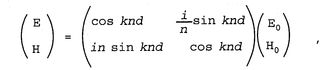
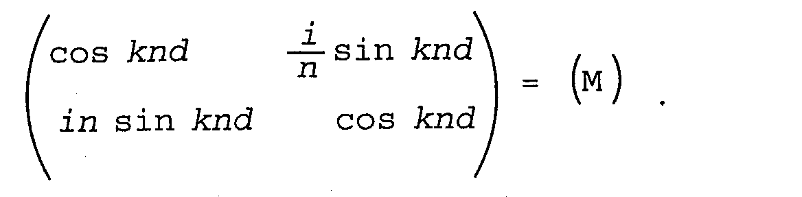
- the matrix (M) is intrinsic to this particular thin film and called the characteristic matrix:
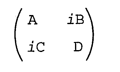
- the product of the matrices can be expressed by a matrix of the same type, which is the characteristic matrix of the laminated thin film for a single cycle:
- the characteristic matrix of an m-cycles laminated film is expressed by the m-th power of the characteristic matrix (M) for a single cycle layer, i.e. (M) m .
- M characteristic matrix
- the wavelength to be used in the inventive flat-plate lens is the wavelength very close to the short wavelength end of this attenuation zone and capable of giving a high transmissivity.
- the periodical structure consists of two layers including a first layer having a refractive index n1 and a thickness d1 and a second layer having a refractive index n2 and a thickness d2
- an almost accurate short wavelength end of the attenuation zone can be obtained by utilizing the approximate expression from the characteristic matrix for a single cycle described above within the range where the ratio (n2 ⁇ d2)/(n1 ⁇ d1) is from about 0.1 to about 10.
- this ratio is 0.01 or smaller or 100 or larger, however, a wavelength value of 0.95 ⁇ or 1.01 ⁇ , respectively, is obtained by a more detailed calculation assuming ⁇ as the wavelength for the periodical structure of a single cycle. It would not be a practical case, however, that one of the two layers has a thickness very much smaller than the other layer.
- Figure 1 is a graphical showing of the short wavelength end by the ratio to the wavelength ⁇ corresponding to the periodical structure under various conditions.
- FIG. 2 is an enlarged cross sectional view showing the structure of a typical optical recording medium utilizing the inventive flat-plate lens.
- the optical recording medium has a laminated structure consisting of a substrate 1 and layers successively formed thereon including a protective layer 2, recording layer 3, protective layer 2a, flat-plate lens layer 4, protective layer 2b, transmission-controlling layer 5 and protective layer 2c.
- This optical recording medium is an example having a transparent or opaque substrate provided thereon with a recording layer of an amorphous material sandwiched by protective layers and further thereon with the flat-plate lens layer and a transmission-controlling layer sandwiched by protective layers. Recording is made by image formation, in the recording layer, of the light coming from the minute light transmitting part formed in the transmission-controlling layer by irradiation of light.
- the recorded images in the recording layer are image-formed on the transmission-controlling layer by means of the flat-plate lens so that the information can be read out through the minute light-transmitting part formed by irradiation with light.
- the performance of the respective layers excepting the flat-plate lens and the principle of information recording and retrieving are the same as in the Super-RENS described in Japanese Patent Kokai 11-250493 and Applied Physics Letters, volume 73, page 2078 (1998).
- the substrates used here were plates of plastic resins or metals having a surface of good planarity of high accuracy.
- a 0.5 mm thick copper plate was used in this Example as the substrate.
- a protective film of SiN was formed in a thickness of 100 nm followed by alternate film formation of each 10 layers of MgF 2 and ZnS, each layer having a thickness of 60 nm.
- a 100 nm thick second protective layer of SiN was formed thereon.
- the procedure for the film formation of these layers was conducted without intermission by using a vacuum film-forming apparatus.
- the layers of MgF 2 and ZnS were formed by using MgF 2 and ZnS, respectively, as the target.
- the inert gas atmosphere of the chamber during film formation was controlled at a pressure of 0.5 Pa.
- the SiN layers were formed by the reactive sputtering method using an Si target in an atmosphere of a mixture of argon and nitrogen gases.
- FIG. 1 shows an enlarged cross sectional view of the thus formed flat-plate lens according to the invention.
- the near-field image of a minute body deposited on the surface of the window portion was image-formed on the opposite side through the flat-plate lens and detected by scanning with an optical probe.
- detailed information was obtained of the minute body deposited in the window portion 6 when detection was made by scanning detection of the image formed on the opposite side through the flat-plate lens with the near-field light emitted from the optical probe.
- a flat-plate lens can be formed on a tough supporting substrate when the substrate is a plate of a plastic resin or a metal having a surface of highly accurate planarity so that the functional performance of the flat-plate lens per se can be utilized through the open window formed in the substrate.
- scanning detection from remote can be undertaken through the flat-plate lens even if the body side is under an environment not suitable for probe scanning detection such as vacuum, solution and the like.
- the protective layers of SiN in the present invention play a role as a separator layer to ensure uniformity of the distance between the body and the flat-plate lens or between the optical probe and the flat-plate lens. While it is possible to adjust the image-forming characteristics of the flat-plate lens by modifying the film thickness of the separator layer, the film thickness can hardly be modified after completion of the film formation.
- the light source is a laser of variable wavelength such as the titanium sapphire laser
- the image-forming characteristics of the flat-plate lens can be optimized by fine adjustment of the wavelength with the distance between the optical probe and the flat-plate lens kept constant.
- a 100 nm thick protective layer of SiN was formed on a 1 mm thick glass plate having planarity of high accuracy as a substrate followed by successive formation of a 15 nm thick masking layer of Sb and a 10 nm thick protective layer of SiN. Further thereon, each 10 layers of MgF 2 and ZnS were alternately formed each in a thickness of 60 nm. Further thereon, a 10 nm thick protective layer of SiN was formed. These film-forming procedures were conducted by using a vacuum film-forming apparatus without intermission. The layers of MgF 2 and ZnS were formed with MgF 2 and ZnS, respectively, as the targets. The pressure of the inert atmosphere was kept at 0.5 Pa during the film-forming procedures. The layers of SiN were formed by the reactive sputtering method in an atmosphere of a gaseous mixture of argon and nitrogen by using a target of Si.
- Figure 4 shows an enlarged cross sectional view of the flat-plate lens prepared in this Example.
- image-formation of the near-field light leaking out of the hole formed by melting of the masking layer of Sb is effected on the opposite side through the flat-plate lens to detect the information corresponding to the image-forming position of the minute body deposited on the protective layer of SiN in the surface.
- melting is accomplished in different positions so that detailed information can be obtained on the minute bodies by scanning detection within allover the scanned ranges.
- Detection of the information can be performed by a method in which the near-field light leaking out of the hole formed by melting is led to the surface of the SiN protective layer by means of the flat-plate lens and the far-field light generated by the interaction thereof with the minute body deposited on the surface is detected at a rearward position to the body or, alternatively, by a method in which detection is performed of the reflecting light re-transmitted through the flat-plate lens and the hole in the melted portion from the substrate side.
- the substrate used here is a substrate bearing information marks recorded in advance thereon.
- the information marks recorded in advance implied above are not limitative provided that the light wave front of an irradiation light can be varied in accordance with the recorded marks of the information including a recording material bearing information recorded in advance, a material on which information is recorded by way of fine ruggedness on a substrate as in ROM disks, and others.
- the information-recorded material used in this Example is a polycarbonate substrate having pit mark ruggedness formed by injection replica-forming method from a fused silica glass plate of good planarity bearing a pit mark pattern formed by the method of electron beam photolithography.
- the recording marks were formed in about 20 nm of ruggedness.
- a 100 nm thick protective layer of SiN was first formed on the substrate and each 10 layers of MgF 2 layers and ZnS layers each having a thickness of 75 nm were alternately formed thereon. Further thereon, a 100 nm thick protective layer of SiN, a 15 nm thick masking layer of Sb and another 100 nm thick protective layer of SiN were successively formed.
- the substrate assembly bearing the thus formed flat-plate lens and a masking layer on a substrate having information marks recorded in advance was rotated at a linear velocity of 6 m/second and incidence of an argon ion laser beam of 488 nm wavelength was made from the protective layer side.
- image formation was made in the Sb masking layer with a numerical aperture of the lens set at 0.6.
- the near-field light leaking out of the hole formed in the melted portion of the Sb masking layer was image-formed on the information recording marks through the flat-plate lens.
- the reflecting light after modulation in accordance with the recorded information marks was detected after passing again through the hole at the melted portion of the Sb masking layer. With incidence of 1.0 mW, signals of 30 MHz corresponding to a mark size of 100 nm could be detected with a C/N larger than 30 db.
- the substrate is made of a plastic resin such as a polycarbonate resin as in this Example, it is optional that, in order to protect the substrate against heating by irradiation with laser beams, to have intervention of a thin metal layer between the substrate and the protective layer. This means is effective also for increasing the reflecting signal light.
- An optical recording medium was prepared by providing a recording layer in place of the marks for information recording in advance in Example 3.
- a 1 mm thick glass substrate of good surface planarity was provided thereon with a 100 nm thick protective layer of SiN followed by successive film formation thereon of a 50 nm thick recording layer of a GeSbTe alloy in an atomic ratio of 2:2:5, a 10 nm thick protective layer of SiN, each 10 alternate layers of MgF 2 and ZnS each having a thickness of 75 nm, a 10 nm thick protective layer of SiN, a 15 nm thick masking layer of Sb and, finally, a 100 nm thick protective layer of SiN.
- the thus prepared optical recording medium was heated and kept standing for 10 minutes at 150 °C, which was slightly higher than the crystallization temperature, followed by cooling down to room temperature to confirm conversion of the recording layer to a crystalline state from the changes in the reflectivity.
- pulse-wise irradiation of the recording medium was effected with light beams of 488 nm wavelength from a 1 W argon ion laser at the substrate side to heat the recording layer up to a temperature instantaneously exceeding the melting temperature followed by causing supercooling utilizing the repose times of the pulses so that the recording layer was confirmed to be subjected to another phase change from the crystalline state to an amorphous state.
- the reflectivity in this time was higher than the reflectivity in the as-deposited condition immediately after preparation of the recording medium but lower than the reflectivity in the aforementioned crystalline state.
- this optical recording medium was irradiated at the protective layer side with argon ion laser beams of 488 nm wavelength.
- Image formation was made here in the Sb masking layer with a numerical aperture 0.6 of the lens.
- the near-field light leaking out of the hole formed by melting of the Sb masking layer was image-formed in the recording layer through the flat-plate lens.
- Recording was made by modulation of the laser power with a single signal of 30 MHz corresponding to a mark length of 100 nm.
- the laser power for recording was 10.0 mW at the moment of pulse-on.
- the optical recording medium having the information marks recorded as above was irradiated at the protective layer side with argon ion laser beams of 488 wavelength.
- image formation was made in the Sb masking layer with a numerical aperture 0.6 of the lens.
- the near-field light leaking out of the hole formed by melting in the Sb masking layer was image-formed on the information recording marks in the recording layer through the flat-plate lens.
- the reflecting light modulated in accordance with the marked information was detected by again passing the melt hole in the Sb masking layer.
- signals of 30 MHz corresponding to a mark size of 100 nm could be detected with a C/N value larger than 30.
- a 1 mm thick glass substrate of good surface planarity was provided on the surface with a 100 nm thick protective layer of SiN followed by successive formation of a 50 nm thick recording layer of a GeSbTe alloy in an atomic ratio of 2:2:5 and a 10 nm thick protective layer of SiN.
- another 1 mm thick glass substrate was provided on the surface with a 100 nm thick protective layer of SiN followed by successive formation of a 15 nm thick masking layer of Sb and a 10 nm thick protective layer of SiN.
- a substrate provided thereon with a masking layer of Sb was coated with an aqueous solution of gelatine in such a coating amount that the gelatine film formed by drying and a hardening treatment at 100 °C for 10 minutes had a thickness of about 10 ⁇ m.
- the gelatine coating film was converted to a bichromic acid-containing gelatine film by dipping in an aqueous bichromic acid solution until sufficient absorption of bichromic acid followed by water rinse and drying.
- the gelatine layer was swelled by dipping in an aqueous solution of D-sorbitol.
- the hologram lattice distance could be controlled by modifying the concentration of the D-sorbitol solution.
- the concentration of the aqueous D-sorbitol solution was gradually increased to find out the turning point from the state of high reflectivity to a state of high transmissivity under vertical incidence of the 488 nm beams.
- the substrate bearing the recording layer prepared as above was brought into direct contact with the thus obtained hologram.
- the peripheral portions of the substrate were consolidated with an adhesive.
- the optical recording medium prepared in this Example was similar to that prepared in Example 4.
- Figure 7 shows an enlarged cross sectional view of the optical recording medium prepared in this Example.
Landscapes
- Engineering & Computer Science (AREA)
- Chemical & Material Sciences (AREA)
- Nanotechnology (AREA)
- Manufacturing & Machinery (AREA)
- Physics & Mathematics (AREA)
- Mathematical Physics (AREA)
- Theoretical Computer Science (AREA)
- Crystallography & Structural Chemistry (AREA)
- Optical Recording Or Reproduction (AREA)
- Diffracting Gratings Or Hologram Optical Elements (AREA)
- Optical Record Carriers And Manufacture Thereof (AREA)
- Optical Head (AREA)
Abstract
Description


Claims (7)
- A flat-plate lens utilizing a thin film layer having a periodical structure corresponding to a wavelength slightly longer than the wavelength used for information recording.
- The flat-plate lens as claimed in claim 1 in which the periodicity of the periodical structure is along the direction of thickness of the flat-plate lens.
- The flat-plate lens as claimed in claim 2 in which the periodical structure is an alternate laminating repetition of films made on a substrate from at least two kinds of substances having different refractive indices each from the other or the others.
- The flat-plate lens as claimed in claim 3 in which the periodical structure is made from two kinds of substances having different refractive indices which are zinc sulfide ZnS and magnesium fluoride MgF2.
- A method for image formation which comprises using the flat-plate lens defined in any one of claims 1 to 4 and forming an image of a body or a light source placed in the proximity of the flat-plate lens or an optical image thereof at the opposite side of the flat-plate lens.
- A method for image formation which comprises using the flat-plate lens defined in any one of claims 1 to 4 and forming an image of a body or a light source positioned in the proximity of the flat-plate lens or an optical image thereof at the opposite side thereto relative to the flat-plate lens by using a reflected light from the flat-plate lens.
- An optical recording medium having a layered structure which comprises a substrate, an optical recording layer and the flat-plate lens defined in any one of claims 1 to 4.
Applications Claiming Priority (2)
| Application Number | Priority Date | Filing Date | Title |
|---|---|---|---|
| JP2002147666 | 2002-05-22 | ||
| JP2002147666A JP4000365B2 (en) | 2002-05-22 | 2002-05-22 | Imaging method using flat lens and high-density optical recording method using the imaging method |
Publications (2)
| Publication Number | Publication Date |
|---|---|
| EP1365394A2 true EP1365394A2 (en) | 2003-11-26 |
| EP1365394A3 EP1365394A3 (en) | 2005-12-21 |
Family
ID=29397854
Family Applications (1)
| Application Number | Title | Priority Date | Filing Date |
|---|---|---|---|
| EP03253171A Withdrawn EP1365394A3 (en) | 2002-05-22 | 2003-05-21 | Flat-plate lens |
Country Status (3)
| Country | Link |
|---|---|
| US (1) | US7099264B2 (en) |
| EP (1) | EP1365394A3 (en) |
| JP (1) | JP4000365B2 (en) |
Families Citing this family (4)
| Publication number | Priority date | Publication date | Assignee | Title |
|---|---|---|---|---|
| US7783140B2 (en) * | 2005-06-09 | 2010-08-24 | Hewlett-Packard Development Company, L.P. | Optically coupled integrated circuit layers |
| US7538858B2 (en) * | 2006-01-11 | 2009-05-26 | Micron Technology, Inc. | Photolithographic systems and methods for producing sub-diffraction-limited features |
| US11808934B2 (en) | 2021-04-20 | 2023-11-07 | Eagle Technology, Llc | Planar optical telescope and related methods |
| CN114355632A (en) * | 2021-12-24 | 2022-04-15 | 中山大学 | Phase-change-material-based flat lens with customized aberration and manufacturing method thereof |
Family Cites Families (7)
| Publication number | Priority date | Publication date | Assignee | Title |
|---|---|---|---|---|
| US4689873A (en) * | 1983-04-28 | 1987-09-01 | Rca Corporation | Imaging device having two anti-reflection layers on a surface of silicon wafer |
| JPH0391128A (en) | 1989-08-31 | 1991-04-16 | Victor Co Of Japan Ltd | Optical recording member |
| JP4613356B2 (en) | 1998-03-03 | 2011-01-19 | 独立行政法人産業技術総合研究所 | Optical recording medium, optical recording method, optical signal reproducing method, optical recording apparatus, and optical signal reproducing apparatus |
| US6404722B1 (en) | 2000-08-01 | 2002-06-11 | Ritek Corporation | Method of increasing recording density and capacity of a compact disc |
| TWI234546B (en) | 2000-08-18 | 2005-06-21 | Ritek Corp | Polysilicon formation method |
| EP1313095B1 (en) * | 2001-11-15 | 2008-10-15 | Samsung Electronics Co. Ltd. | Compatible optical pickup |
| AU2002319530A1 (en) | 2001-11-16 | 2003-06-10 | Marconi Uk Intellectual Property Ltd | Multilayer imaging device with negativer permittivity or negative permeability layers |
-
2002
- 2002-05-22 JP JP2002147666A patent/JP4000365B2/en not_active Expired - Lifetime
-
2003
- 2003-05-21 EP EP03253171A patent/EP1365394A3/en not_active Withdrawn
- 2003-05-21 US US10/442,213 patent/US7099264B2/en not_active Expired - Fee Related
Also Published As
| Publication number | Publication date |
|---|---|
| US20040047272A1 (en) | 2004-03-11 |
| US7099264B2 (en) | 2006-08-29 |
| JP2003344627A (en) | 2003-12-03 |
| JP4000365B2 (en) | 2007-10-31 |
| EP1365394A3 (en) | 2005-12-21 |
Similar Documents
| Publication | Publication Date | Title |
|---|---|---|
| KR100946009B1 (en) | Resist Materials and Micromachining Methods | |
| US5424106A (en) | Optical information recording medium and method of designing its structure | |
| EP1551020B1 (en) | Method of producing optical disk-use original and method of producing optical disk | |
| US6226258B1 (en) | Optical recording medium with transmissivity controlling layer | |
| JP3284744B2 (en) | Optical information recording medium | |
| JP3154295B2 (en) | Optical storage device | |
| EP0108457B1 (en) | Method for the production of an optical recording element | |
| JP3743782B2 (en) | Fine pattern forming material and fine pattern forming method using the same | |
| JP3879726B2 (en) | Manufacturing method of optical disc master and manufacturing method of optical disc | |
| US7099264B2 (en) | Flat-plate lens | |
| US20050219994A1 (en) | Optical recording medium | |
| JP2003051137A (en) | Information recording medium | |
| JP2889880B2 (en) | Laminate, compound used for laminate, and optical information carrier having laminate | |
| EP1548722A1 (en) | Optical information recording medium and method for manufacturing same | |
| Koronkevich et al. | Laser thermochemical technology for synthesizing optical diffraction elements utilizing chromium films | |
| JPH07161071A (en) | Optical recording medium | |
| JP2007264657A (en) | Flat lens and optical recording medium using the flat lens | |
| JPH04232780A (en) | Phase change optical recording medium | |
| JPH01251342A (en) | Information recording medium | |
| JP2523904B2 (en) | Recording medium and optical disc using the same | |
| JP2001243667A (en) | Manufacturing method of optical recording medium | |
| JPH01251338A (en) | Information recording medium | |
| JP2003019868A5 (en) | ||
| Zhang et al. | Readout of super-resolution marks with Ti thin film | |
| JPH01251336A (en) | Information recording medium |
Legal Events
| Date | Code | Title | Description |
|---|---|---|---|
| PUAI | Public reference made under article 153(3) epc to a published international application that has entered the european phase |
Free format text: ORIGINAL CODE: 0009012 |
|
| AK | Designated contracting states |
Kind code of ref document: A2 Designated state(s): AT BE BG CH CY CZ DE DK EE ES FI FR GB GR HU IE IT LI LU MC NL PT RO SE SI SK TR |
|
| AX | Request for extension of the european patent |
Extension state: AL LT LV MK |
|
| PUAL | Search report despatched |
Free format text: ORIGINAL CODE: 0009013 |
|
| AK | Designated contracting states |
Kind code of ref document: A3 Designated state(s): AT BE BG CH CY CZ DE DK EE ES FI FR GB GR HU IE IT LI LU MC NL PT RO SE SI SK TR |
|
| AX | Request for extension of the european patent |
Extension state: AL LT LV MK |
|
| AKX | Designation fees paid | ||
| REG | Reference to a national code |
Ref country code: DE Ref legal event code: 8566 |
|
| STAA | Information on the status of an ep patent application or granted ep patent |
Free format text: STATUS: THE APPLICATION IS DEEMED TO BE WITHDRAWN |
|
| 18D | Application deemed to be withdrawn |
Effective date: 20060622 |