EP1365333A1 - Method and system for designing circuit layout - Google Patents
Method and system for designing circuit layout Download PDFInfo
- Publication number
- EP1365333A1 EP1365333A1 EP02700794A EP02700794A EP1365333A1 EP 1365333 A1 EP1365333 A1 EP 1365333A1 EP 02700794 A EP02700794 A EP 02700794A EP 02700794 A EP02700794 A EP 02700794A EP 1365333 A1 EP1365333 A1 EP 1365333A1
- Authority
- EP
- European Patent Office
- Prior art keywords
- quasi
- circuit
- layout design
- stationary
- closed circuits
- Prior art date
- Legal status (The legal status is an assumption and is not a legal conclusion. Google has not performed a legal analysis and makes no representation as to the accuracy of the status listed.)
- Withdrawn
Links
Images





Classifications
-
- G—PHYSICS
- G06—COMPUTING OR CALCULATING; COUNTING
- G06F—ELECTRIC DIGITAL DATA PROCESSING
- G06F30/00—Computer-aided design [CAD]
- G06F30/30—Circuit design
- G06F30/39—Circuit design at the physical level
-
- G—PHYSICS
- G06—COMPUTING OR CALCULATING; COUNTING
- G06F—ELECTRIC DIGITAL DATA PROCESSING
- G06F30/00—Computer-aided design [CAD]
- G06F30/30—Circuit design
- G06F30/36—Circuit design at the analogue level
- G06F30/367—Design verification, e.g. using simulation, simulation program with integrated circuit emphasis [SPICE], direct methods or relaxation methods
Definitions
- the present invention relates to a circuit layout design method and a system for the circuit layout design method. More specifically, the present invention relates to a circuit layout design method for a digital printed circuit board and an LSI (large scale integrated) circuit on which high-speed, high-frequency circuit devices are mainly mounted.
- LSI large scale integrated
- an LSI circuit design system and a printed circuit board (PCB) circuit design system have existed independently of each other, and an integrated EDA (electronic design automation) system from the LSI to the PCB has not existed.
- EDA electronic design automation
- an object of the present invention to provide a circuit layout design method and a circuit layout design system capable of designing an LSI circuit and an electronic circuit board free of electromagnetic interference.
- a circuit layout design method including: a quasi-stationary circuit reduction step of dividing an entire circuit represented by a net list and a part library into a plurality of quasi-stationary closed circuits having a reduced size so that an intensity of an electromagnetic wave radiated from each of the quasi-stationary closed circuits is not more than a predetermined value; and a wiring constraint condition calculation step of calculating constraint conditions for wirings mutually connecting the plurality of quasi-stationary closed circuits so that the intensity of the electromagnetic wave radiated from each of the wirings is not more than a predetermined value.
- the circuit layout design method may further include a layout step of laying out parts and the wirings based on the net list and the parts library while keeping the constraint conditions.
- the quasi-stationary circuit reduction step and the wiring constraint condition calculation step may be executed for each of frequencies in a descending order and executed so that each of the quasi-stationary closed circuits for a certain frequency includes one or more the quasi-stationary closed circuits for a higher frequency than the certain frequency.
- the constraint conditions may include at least a maximum wiring length.
- the quasi-stationary circuit reduction step may include steps of: obtaining a current waveform by a SPICE (a simulation program with integrated circuit emphasis) using a power supply terminal model and one of an IBIS (I/O buffer information specification) model and an IMIC (I/O interface model for integrated circuit) model; Fourier-transforming the current waveform to a current spectrum; and calculating a field intensity spectrum at a distance by dipole antenna radiation or electromagnetic analysis using the current spectrum.
- SPICE a simulation program with integrated circuit emphasis
- IBIS I/O buffer information specification
- IMIC I/O interface model for integrated circuit
- the circuit layout design method may be used for layout design of a printed circuit board.
- the circuit layout design method may be used for layout design of a semiconductor device.
- the circuit layout design method may be used for integrated design of a semiconductor device and a printed circuit board.
- the present invention incorporates a completely new concept of the quasi-stationary closed circuit (QSCC) into design tools (such as a simulator and a layout CAD) for a digital printed circuit board and a semiconductor LSI.
- QSCC quasi-stationary closed circuit
- Fig. 1 is a conceptual view of the best mode embodiment of a circuit layout design system according to the present invention. This conceptual view includes main constituent elements which can be applied to both the semiconductor LSI design and the circuit layout design.
- the circuit layout design system 1 consists of a QSCC database 2, a QSCC grouping & database extraction analysis tool (to be referred to as "QSCC designer" hereinafter) 3, a layout CAD 4 and a parts library 5.
- the QSCC database 2 directly stores rules which satisfy the QSCC concept which are extracted by experts in electromagnetic interference problems through experiment, analysis or the like, or the QSCC database 2 stores rules analyzed/extracted by the QSCC designer 3.
- the libraries (QSCC rules) stored in the QSCC database 2 are constraint conditions which are set when the layout CAD 4 makes layout and wiring design.
- a semiconductor LSI or printed circuit board (PCB) designed not to violate the rules (restrictions) satisfies the requirements of the QSCC rules and thus realizes electromagnetic interference free design.
- the QSCC database 2 stores libraries on the allowable maximum wiring length between the QSCC blocks, a line form and the like.
- Fig. 2 is a detailed block diagram of the most preferred embodiment of the circuit layout design system according to the present invention. Although the block diagram of Fig. 2 shows the system for printed circuit board (PCB) design, a system for LSI design is basically similar in configuration to the system shown in Fig. 2.
- PCB printed circuit board
- the circuit layout design system 1 consists of the QSCC database 2, the QSCC designer 3, the layout CAD 4, the parts library 5, a high-rate EMI simulator 6 and a circuit diagram editor 7.
- the QSCC designer 3 inputs a net list which indicates the logic connection of the respective circuit constituent elements and which is supplied from the circuit diagram editor 7 which designs a logic circuit, an IBIS model and an IMIC model (signal terminal) for each semiconductor LSI terminal stored in the parts library 5, and a power supply model as disclosed in Document 4, and extracts QSCC design conditions so as to group the QSCC on a digital circuit and to give restrictions to the placement of parts and routing of parts and the like performed by the layout CAD 4.
- the data extracted by the QSCC designer 3 is stored in the QSCC database 2.
- the QSCC database 2 is connected to the layout CAD 4.
- the layout CAD 4 executes electromagnetic interference free design while referring to the QSCC database 2, thereby designing the printed circuit board (PCB) 8 based on the QSCC concept.
- the CAD data designed by the layout CAD 4 is transferred to the high-rate EMI simulator 6 through a specific interface, and electromagnetic radiation noise is analyzed by the simulator 6 for final design inspection. Further, it is necessary to measure the electric field intensity of the printed circuit board (PCB) 8 manufactured using the layout CAD 4 in a qualified radio wave darkroom or an open site so as to determine whether the PCB 8 satisfies the international or domestic EMI standard. Therefore, it is effective to analyze the electromagnetic radiation noise by the high-rate EMI simulator 6 in advance for real-time inspection for the design.
- PCB printed circuit board
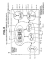
- Fig. 3 is a typical view showing one example of grouping overall devices on the printed circuit board (PCB) 8 to QSCC blocks.
- the minimum unit of the QSCC blocks is an LSI and LISs on the PCB 8 are grouped according to three frequencies.
- the LSIs are grouped into QSCC blocks 10-1 (high-rate blocks) in the highest hierarchy according to the highest frequency among the three frequencies using an algorithm according to the present invention (see Figs. 7 and 8 to be described later).
- the LSIs are grouped according to the second highest frequency (intermediate-rate frequency) to thereby generate larger QSCC blocks 10-2 than the QSCC blocks 10-1.
- the LSIs are grouped according to the lowest frequency to thereby generate larger QSCC blocks 10-3 than the QSCC blocks 10-2.
- the LSIs are grouped according to the three frequencies.
- the number of points of analysis frequencies used for grouping is not limited to three but may be any arbitrary number.
- the grouping of the LSIs into the QSCC blocks is executed in a plurality of hierarchies according to operating frequencies and the grouping is continued until all the LSIs mounted on the printed circuit board (PCB) 8 are included in one QSCC block.
- the transmission lines are classified to signal wirings and power supply wirings (noted that the power supply circuit has a default to be wired as stated above).
- the recent study obviously shows that the greatest cause of the electromagnetic interference derived from digital equipment lies in the power supply circuit. Therefore, by adopting line components that decrease the impedance of the power supply line in the high frequency range as described in the invention (Document 3) of the applicant of the present application so as to intensify decoupling for the power supply wirings which are the greatest cause of the electromagnetic interference, it is possible to efficiently, considerably suppress the electromagnetic interference from the power supply line. Accordingly, it suffices to execute designing the PCB 8 while paying greater attention to the electromagnetic interference from the signal wirings.
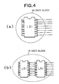
- Fig. 4 is a typical view showing examples of the QSCC blocks.
- Fig. 4 shows a case in which the minimum unit of the QSCC blocks is an LSI.
- a QSCC block consists of one LSI (see Fig. (a)) or a plurality of (two in Fig. 4(b)) LSIs.
- Fig. 5 is a typical view showing one example of extending the minimum units of the QSCC blocks from the LSI to functional blocks in the LSI. It is estimated that if the rate of a semiconductor device is rapidly accelerated and shifting to an SOC (System on Chip), then it is difficult to create QSCC blocks according to the units of the LSIs and it is, therefore, necessary to form QSCC blocks according to smaller units, i.e., the internal elements of the LSI.
- SOC System on Chip
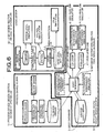
- Fig. 6 shows the concept of a design flow executed by the circuit layout design system according to the present invention.
- the organic connection between the process/device design section 11 and the logic design section 12 has not been established as the integrated EDA system and no drastic electromagnetic interference free design rules have been, therefore, established.
- the process design section 11 can be connected to the logic design section 12 as the integrated EDA system and electromagnetic interference free design can be realized.
- the QSCC designer 3 plays a central role in the circuit layout design system 1.
- the QSCC designer 3 executes layout design and wiring design based on various QSCC libraries (rules) stored in the QSCC database 2 and the high-rate EMI simulator 6 executes real-time inspection and analysis for the design.
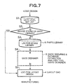
- Fig. 7 is a schematic diagram showing an entire QSCC design flow
- Fig. 8 is a schematic diagram showing a design flow executed by the QSCC designer 3.
- the QSCC design flow will first be described. Referring to Fig. 7, a net list is extracted from the logic design data (in a step S1), and it is searched whether the device (i.e., the QSCC block) is already registered with the parts library 5 (in a step S2). If it is already registered ("Yes" in the step S2), it means that rules satisfying the QSCC requirements exist. Therefore, the processing moves to layout design executed by the layout CAD 4 (a step S5).
- the device is not registered with the parts library 5 ("No" in the step S2), the device is registered as a new device with the library 5 (in a step S3).
- the processing moves to a step executed by the QSCC designer 3, which adds QSCC rules (a step S4), and the processing then moves to a step executed by the layout design section (a step S5).
- the QSCC rules analyzed by the QSCC designer 3 are stored in the QSCC database 2 and used as later design information.
- the basic functions of the QSCC designer 3 include a function of grouping the devices into QSCC blocks based on a certain algorithm, a function of analyzing the electromagnetic interference of the transmission lines connecting the QSCC blocks, extracting parameters (e.g., a maximum allowable line length) to be set as CAD design constraint conditions, and registering the extracted parameters with the database.
- the basic functions of the QSCC designer 3 include a function of grouping the devices into QSCC blocks based on a certain algorithm, a function of analyzing the electromagnetic interference of the transmission lines connecting the QSCC blocks, extracting parameters (e.g., a maximum allowable line length) to be set as CAD design constraint conditions, and registering the extracted parameters with the database.
- Fig. 8 shows an example in which the LSI is a minimum unit of the QSCC blocks.
- an LSI that operates at the highest clock is assumed as the highest class (hierarchy) QSCC (in a step S11).
- the current waveforms of the wirings between the QSCC blocks are obtained by the SPICE (in a step S12).
- the current waveform analyzed by the SPICE is subjected to Fourier transform using the IBIS model (or IMIC model) (signal terminal) and the NEC power supply model (power supply terminal) for each terminal of the LSIs stored in the parts library 5, and a current spectrum is obtained.
- a field intensity spectrum at a distant location is calculated by dipole antenna radiation or electromagnetic field analysis (in a step S13).
- This electromagnetic field analysis transmission line analysis
- a highly accurate distant field intensity is calculated.
- the reason for using the dipole antenna radiation is that normal mode (differential mode) radiation is basically not present or negligibly small on an ideal transmission line (e.g., a micro-strip line). This is because a current carried across the line also flows as a feedback current on a flat plane, such as a closest ground layer, with an opposite phase, so that electromagnetic fields cancel each other.
- a standard tolerance which is an international standard of CISPR22 ITE Class B in the example of Fig. 8
- a certain margin XdB variable
- a step S14 it is determined whether the radiation from the line satisfies a standard tolerance (which is an international standard of CISPR22 ITE Class B in the example of Fig. 8) with a certain margin XdB (variable) (in a step S14). If the field intensity spectrum obtained falls within the range of 'tolerance + margin' ("Yes" in the step S14), an allowable maximum wiring length between the QSCC blocks is calculated (in a step S15). The maximum allowable wiring length can be easily calculated based on the parameters for the dipole antenna radiation. The LSIs can be thus grouped into the QSCC block in that class. Thereafter, the grouping class information and the maximum wiring length are stored in the QSCC database 2 (in a step S17).
- a standard tolerance which is an international standard of CISPR22 ITE Class B in the example of
- LSIs devices on the circuit fall within one QSCC block of the QSCC database 2 (in a step S18). If all the devices belongs to one QSCC block ('Yes" in the step S18), a signal line structure and a wiring line structure satisfying QSCC rules for the corresponding class are selected from the parts library 5 (in a step S19) and the processing moves to CAD design.
- the QSCC class is degraded by one rank (i.e., a clock frequency is lowered by one rank) and the QSCC block is assumed (in a step S20).
- devices are grouped into a plurality of QSCC hierarchies (QSCC classes) according to clock frequencies.
- QSCC classes QSCC classes
- the devices are grouped according to the class of the highest hierarchy (the highest clock frequency). If the entire circuit is not contained in one QSCC, grouping is re-executed in a hierarchy (clock frequency) degraded by one rank. The same routine is repeated until all the devices on the circuit belong to one QSCC.
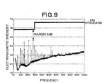
- Fig. 9 shows one example of an electric field spectrum as a result of the electromagnetic field analysis.
- Fig. 9 shows the definition of the margin relative to an EMI standard value. Namely, the EMI standard value shown in Fig. 9 corresponds to the "tolerance” (see the step S14) and "tolerance + margin X" corresponds to a field intensity lower than this EMI standard value by XdB.
- Fig. 10 shows one example of the QSCC database 2.
- This database 2 is an example of the database in a case in which an LSI is the minimum unit of the QSCC blocks.
- the QSCC database 2 takes a form of the parts list created for the terminals of each LSI and includes QSCC conditions allocated to each terminal of each LSI.
- the database 2 is connected to the layout CAD 4 and the conditions in the database 2 are used by the layout CAD 4 as those for giving some restrictions to parts placement design, wiring design and the like from QSCC viewpoints.
- FIG. 10 an example of allocating an allowable maximum line length, a line form and a line width to each terminal of each LSI is shown. However, the conditions are not limited thereto.
- a control program shown in the flow charts of Figs. 7 and 8 can be recorded on a recording medium (not shown) in advance and read from the recording medium to an external processor (not shown) and that the above-stated circuit layout design method can be executed by the QSCC designer 3, the layout CAD 4, the circuit diagram editor 7 and the high-rate EMI simulator 6 according to the control program.
- the present invention can be utilized for the design of the LSI circuit, the electronic circuit board and the like which are free of electromagnetic interference.
Landscapes
- Engineering & Computer Science (AREA)
- Computer Hardware Design (AREA)
- Physics & Mathematics (AREA)
- Theoretical Computer Science (AREA)
- Evolutionary Computation (AREA)
- Geometry (AREA)
- General Engineering & Computer Science (AREA)
- General Physics & Mathematics (AREA)
- Microelectronics & Electronic Packaging (AREA)
- Design And Manufacture Of Integrated Circuits (AREA)
Abstract
A circuit layout design method capable of an LSI circuit or an
electronic printed circuit board free of electromagnetic interference is
provided. The layout design method according to the invention includes a
quasi-stationary circuit reduction step of deviding an entire circuit
represented by a net list and a part library into a plurality of
quasi-stationary closed circuits having a reduced size so that an intensity of
an electromagnetic wave radiated from each of the quasi-stationary closed
circuits is not more than a predetermined value; a wiring constraint
condition calculation step of calculating constraint conditions for each of
wirings mutually connecting the plurality of quasi-stationary closed circuits
so that the intensity of the electromagnetic wave radiated from each of the
wirings is not more than the predetermined value; and a layout step of
laying out parts and the wirings based on the net list and the parts library
so as to satisfy the constraint conditions.
Description
The present invention relates to a circuit layout design method and
a system for the circuit layout design method. More specifically, the
present invention relates to a circuit layout design method for a digital
printed circuit board and an LSI (large scale integrated) circuit on which
high-speed, high-frequency circuit devices are mainly mounted.
As for the conventional digital circuit design system, an LSI circuit
design system and a printed circuit board (PCB) circuit design system have
existed independently of each other, and an integrated EDA (electronic
design automation) system from the LSI to the PCB has not existed.
In addition, in the process of the LSI design, no organic connection
has been established between process design and logic design and no
consistent integrated system has existed. Although information such as
know-how's have been provided to take measures against EMI
(electromagnetic interference), no consideration has been given to such an
electromagnetic free design technique as to be able to be incorporated into
the EDA design system.
Meanwhile, in relation to the printed circuit board circuit design
system, a simplified design check tool such as an EMI rule checker has
existed; however, no basic design rules have been established.
A conventional design technique in relation to a technique for
suppressing digital equipment electromagnetic interference will next be
described.
The digitization of electronic equipment increasingly progresses.
For a logic design region, which occupies large parts of electronic equipment
design, CAE (Computer Aided Engineering) design covering design through
manufacturing widely spreads and greatly contributes to the improvement
of the quality and efficiency of design and manufacturing. However, for a
so-called electronic SI (Signal Integrity) region which occupies the
remaining parts of the electronic equipment design and which includes
packaging, structure, wiring and the like; there is a tendency to rely on the
discretion of an engineer involved in design. As a result, an integrated
optimum design method for covering design through manufacturing has not
been established. In light of the present situations, the conventional arts 1
and 2 (Documents 1 and 2) have the following problems.
It is, therefore, an object of the present invention to provide a circuit
layout design method and a circuit layout design system capable of
designing an LSI circuit and an electronic circuit board free of
electromagnetic interference.
According to the present invention, there is provided a circuit layout
design method including: a quasi-stationary circuit reduction step of
dividing an entire circuit represented by a net list and a part library into a
plurality of quasi-stationary closed circuits having a reduced size so that an
intensity of an electromagnetic wave radiated from each of the
quasi-stationary closed circuits is not more than a predetermined value; and
a wiring constraint condition calculation step of calculating constraint
conditions for wirings mutually connecting the plurality of quasi-stationary
closed circuits so that the intensity of the electromagnetic wave radiated
from each of the wirings is not more than a predetermined value.
The circuit layout design method may further include a layout step
of laying out parts and the wirings based on the net list and the parts
library while keeping the constraint conditions.
In the circuit layout design method, the quasi-stationary circuit
reduction step and the wiring constraint condition calculation step may be
executed for each of frequencies in a descending order and executed so that
each of the quasi-stationary closed circuits for a certain frequency includes
one or more the quasi-stationary closed circuits for a higher frequency than
the certain frequency.
In the circuit layout design method, the constraint conditions may
include at least a maximum wiring length.
In the circuit layout design method, the quasi-stationary circuit
reduction step may include steps of: obtaining a current waveform by a
SPICE (a simulation program with integrated circuit emphasis) using a
power supply terminal model and one of an IBIS (I/O buffer information
specification) model and an IMIC (I/O interface model for integrated circuit)
model; Fourier-transforming the current waveform to a current spectrum;
and calculating a field intensity spectrum at a distance by dipole antenna
radiation or electromagnetic analysis using the current spectrum.
The circuit layout design method may be used for layout design of a
printed circuit board.
The circuit layout design method may be used for layout design of a
semiconductor device.
The circuit layout design method may be used for integrated design
of a semiconductor device and a printed circuit board.
The outline of the present invention will first be described.
To attain the above-stated object, the present invention incorporates
a completely new concept of the quasi-stationary closed circuit (QSCC) into
design tools (such as a simulator and a layout CAD) for a digital printed
circuit board and a semiconductor LSI.
The concept of the QSCC that the present invention proposes for the
first time for design method free of an electromagnetic interference for
digital equipment will be described. Generally, if the wavelength λ of a
circuit current is sufficiently large as compared with the size of a closed
circuit, electromagnetic radiation is eliminated. In other words, in order to
realize a device free of mutual electromagnetic interference problems, it is
effective to design all closed circuits to have quasi-stationary states.
The embodiment of the present invention will next be described with
reference to the accompanying drawings. Fig. 1 is a conceptual view of the
best mode embodiment of a circuit layout design system according to the
present invention. This conceptual view includes main constituent
elements which can be applied to both the semiconductor LSI design and the
circuit layout design. Referring to Fig. 1, the circuit layout design system 1
consists of a QSCC database 2, a QSCC grouping & database extraction
analysis tool (to be referred to as "QSCC designer" hereinafter) 3, a layout
CAD 4 and a parts library 5.
The QSCC database 2 directly stores rules which satisfy the QSCC
concept which are extracted by experts in electromagnetic interference
problems through experiment, analysis or the like, or the QSCC database 2
stores rules analyzed/extracted by the QSCC designer 3. The libraries
(QSCC rules) stored in the QSCC database 2 are constraint conditions
which are set when the layout CAD 4 makes layout and wiring design. A
semiconductor LSI or printed circuit board (PCB) designed not to violate the
rules (restrictions) satisfies the requirements of the QSCC rules and thus
realizes electromagnetic interference free design. To be specific, the QSCC
database 2 stores libraries on the allowable maximum wiring length
between the QSCC blocks, a line form and the like.
Fig. 2 is a detailed block diagram of the most preferred embodiment
of the circuit layout design system according to the present invention.
Although the block diagram of Fig. 2 shows the system for printed circuit
board (PCB) design, a system for LSI design is basically similar in
configuration to the system shown in Fig. 2.
Referring to Fig. 2, the circuit layout design system 1 consists of the
QSCC database 2, the QSCC designer 3, the layout CAD 4, the parts library
5, a high-rate EMI simulator 6 and a circuit diagram editor 7.
The QSCC designer 3 inputs a net list which indicates the logic
connection of the respective circuit constituent elements and which is
supplied from the circuit diagram editor 7 which designs a logic circuit, an
IBIS model and an IMIC model (signal terminal) for each semiconductor LSI
terminal stored in the parts library 5, and a power supply model as
disclosed in Document 4, and extracts QSCC design conditions so as to
group the QSCC on a digital circuit and to give restrictions to the placement
of parts and routing of parts and the like performed by the layout CAD 4.
The data extracted by the QSCC designer 3 is stored in the QSCC
database 2. The QSCC database 2 is connected to the layout CAD 4. The
layout CAD 4 executes electromagnetic interference free design while
referring to the QSCC database 2, thereby designing the printed circuit
board (PCB) 8 based on the QSCC concept.
On the other hand, the CAD data designed by the layout CAD 4 is
transferred to the high-rate EMI simulator 6 through a specific interface,
and electromagnetic radiation noise is analyzed by the simulator 6 for final
design inspection. Further, it is necessary to measure the electric field
intensity of the printed circuit board (PCB) 8 manufactured using the layout
CAD 4 in a qualified radio wave darkroom or an open site so as to determine
whether the PCB 8 satisfies the international or domestic EMI standard.
Therefore, it is effective to analyze the electromagnetic radiation noise by
the high-rate EMI simulator 6 in advance for real-time inspection for the
design.
To extract the power supply model of the semiconductor LSI stored
in the parts library 5 (as described in Document 4), there are an extraction
method by transforming the SPICE model of the LSI itself and an extraction
method by measuring the high frequency power supply current spectrum of
the LSI using a magnetic field (current) probe, transforming the measured
spectrum to a time-axis waveform, and thereby constructing a model.
Fig. 3 is a typical view showing one example of grouping overall
devices on the printed circuit board (PCB) 8 to QSCC blocks. In Fig. 3, the
minimum unit of the QSCC blocks is an LSI and LISs on the PCB 8 are
grouped according to three frequencies. Referring to Fig. 3, the LSIs are
grouped into QSCC blocks 10-1 (high-rate blocks) in the highest hierarchy
according to the highest frequency among the three frequencies using an
algorithm according to the present invention (see Figs. 7 and 8 to be
described later). Next, with the resultant QSCC blocks 10-1 according to
the highest frequency set as units, the LSIs are grouped according to the
second highest frequency (intermediate-rate frequency) to thereby generate
larger QSCC blocks 10-2 than the QSCC blocks 10-1. Finally, with the
QSCC blocks 10-2 set as units, the LSIs are grouped according to the lowest
frequency to thereby generate larger QSCC blocks 10-3 than the QSCC
blocks 10-2.
In this example, the LSIs are grouped according to the three
frequencies. However, the number of points of analysis frequencies used
for grouping is not limited to three but may be any arbitrary number.
According to the concept of the quasi-stationary closed circuit
(QSCC) stated above, it is obvious that the higher the frequency is, the
smaller the sizes of the QSCC blocks become. In this way, the grouping of
the LSIs into the QSCC blocks is executed in a plurality of hierarchies
according to operating frequencies and the grouping is continued until all
the LSIs mounted on the printed circuit board (PCB) 8 are included in one
QSCC block.
According to the QSCC theory, there is no electromagnetic radiation
from each QSCC block and it suffices to consider only electromagnetic
radiation from the respective lines connecting the QSCC blocks. Due to
this, radiation from each transmission line is analyzed, and the PCB 8 is
designed based on the restrictions to the layout and wiring design so as to
satisfy an EMI standard value with a certain margin, whereby the entire
printed circuit board (PCB) 8 free of electromagnetic interference is
designed.
Further, the transmission lines are classified to signal wirings and
power supply wirings (noted that the power supply circuit has a default to
be wired as stated above). The recent study obviously shows that the
greatest cause of the electromagnetic interference derived from digital
equipment lies in the power supply circuit. Therefore, by adopting line
components that decrease the impedance of the power supply line in the
high frequency range as described in the invention (Document 3) of the
applicant of the present application so as to intensify decoupling for the
power supply wirings which are the greatest cause of the electromagnetic
interference, it is possible to efficiently, considerably suppress the
electromagnetic interference from the power supply line. Accordingly, it
suffices to execute designing the PCB 8 while paying greater attention to
the electromagnetic interference from the signal wirings.
Fig. 4 is a typical view showing examples of the QSCC blocks. Fig.
4 shows a case in which the minimum unit of the QSCC blocks is an LSI.
Depending on the operating frequency of the LSI, a QSCC block consists of
one LSI (see Fig. (a)) or a plurality of (two in Fig. 4(b)) LSIs.
Fig. 5 is a typical view showing one example of extending the
minimum units of the QSCC blocks from the LSI to functional blocks in the
LSI. It is estimated that if the rate of a semiconductor device is rapidly
accelerated and shifting to an SOC (System on Chip), then it is difficult to
create QSCC blocks according to the units of the LSIs and it is, therefore,
necessary to form QSCC blocks according to smaller units, i.e., the internal
elements of the LSI. Although the drawings and the description of the
specification are centered on the example of setting an LSI as the minimum
unit of the QSCC blocks, the minimum unit of the QSCC blocks is not
limited to the LSI but may be the internal functional block of the LSI as
shown in Fig. 5.
Fig. 6 shows the concept of a design flow executed by the circuit
layout design system according to the present invention. Conventionally,
the organic connection between the process/device design section 11 and the
logic design section 12 has not been established as the integrated EDA
system and no drastic electromagnetic interference free design rules have
been, therefore, established.
In the circuit layout design system 1 according to the present
invention, by contrast, the process design section 11 can be connected to the
logic design section 12 as the integrated EDA system and electromagnetic
interference free design can be realized. In addition, the QSCC designer 3
plays a central role in the circuit layout design system 1. The QSCC
designer 3 executes layout design and wiring design based on various QSCC
libraries (rules) stored in the QSCC database 2 and the high-rate EMI
simulator 6 executes real-time inspection and analysis for the design.
Fig. 7 is a schematic diagram showing an entire QSCC design flow,
and Fig. 8 is a schematic diagram showing a design flow executed by the
QSCC designer 3. The QSCC design flow will first be described.
Referring to Fig. 7, a net list is extracted from the logic design data (in a
step S1), and it is searched whether the device (i.e., the QSCC block) is
already registered with the parts library 5 (in a step S2). If it is already
registered ("Yes" in the step S2), it means that rules satisfying the QSCC
requirements exist. Therefore, the processing moves to layout design
executed by the layout CAD 4 (a step S5). If the device is not registered
with the parts library 5 ("No" in the step S2), the device is registered as a
new device with the library 5 (in a step S3). The processing moves to a step
executed by the QSCC designer 3, which adds QSCC rules (a step S4), and
the processing then moves to a step executed by the layout design section (a
step S5). The QSCC rules analyzed by the QSCC designer 3 are stored in
the QSCC database 2 and used as later design information.
Next, the design flow executed by the QSCC designer 3 shown in Fig.
8 will be described. Referring to Fig. 8, the basic functions of the QSCC
designer 3 include a function of grouping the devices into QSCC blocks
based on a certain algorithm, a function of analyzing the electromagnetic
interference of the transmission lines connecting the QSCC blocks,
extracting parameters (e.g., a maximum allowable line length) to be set as
CAD design constraint conditions, and registering the extracted parameters
with the database.
It is noted that Fig. 8 shows an example in which the LSI is a
minimum unit of the QSCC blocks. First, an LSI that operates at the
highest clock is assumed as the highest class (hierarchy) QSCC (in a step
S11). Then, the current waveforms of the wirings between the QSCC
blocks are obtained by the SPICE (in a step S12). To obtain a current
waveform, the current waveform analyzed by the SPICE is subjected to
Fourier transform using the IBIS model (or IMIC model) (signal terminal)
and the NEC power supply model (power supply terminal) for each terminal
of the LSIs stored in the parts library 5, and a current spectrum is obtained.
When the current spectrum is obtained, a field intensity spectrum at
a distant location (e.g., at a distance of 10m) is calculated by dipole antenna
radiation or electromagnetic field analysis (in a step S13). Through this
electromagnetic field analysis (transmission line analysis), a highly accurate
distant field intensity is calculated. The reason for using the dipole
antenna radiation is that normal mode (differential mode) radiation is
basically not present or negligibly small on an ideal transmission line (e.g.,
a micro-strip line). This is because a current carried across the line also
flows as a feedback current on a flat plane, such as a closest ground layer,
with an opposite phase, so that electromagnetic fields cancel each other.
However, it does not necessarily mean that 100% of the normal mode
current returns as the feedback current but only part of the normal mode
current is transformed to a common mode current, which causes common
mode radiation which is said to dominate the electromagnetic radiation.
This is why the electric dipole antenna radiation which can approximate the
common mode radiation is utilized.
Next, it is determined whether the radiation from the line satisfies a
standard tolerance (which is an international standard of CISPR22 ITE
Class B in the example of Fig. 8) with a certain margin XdB (variable) (in a
step S14). If the field intensity spectrum obtained falls within the range of
'tolerance + margin' ("Yes" in the step S14), an allowable maximum wiring
length between the QSCC blocks is calculated (in a step S15). The
maximum allowable wiring length can be easily calculated based on the
parameters for the dipole antenna radiation. The LSIs can be thus
grouped into the QSCC block in that class. Thereafter, the grouping class
information and the maximum wiring length are stored in the QSCC
database 2 (in a step S17).
On the other hand, if the field intensity spectrum does not fall
within the range of 'tolerance + margin' ("No" in the step S14), QSCC
grouping scale is reduced. The processing returns to the step S12 and the
electromagnetic field analysis is re-executed (in a step S16). The
processing is continued while reducing the QSCC grouping scale until the
field intensity spectrum belongs to one QSCC block in the class.
If grouping in certain classes (in the descending order of hierarchy)
is completed, it is determined whether all the devices (LSIs) on the circuit
fall within one QSCC block of the QSCC database 2 (in a step S18). If all
the devices belongs to one QSCC block ('Yes" in the step S18), a signal line
structure and a wiring line structure satisfying QSCC rules for the
corresponding class are selected from the parts library 5 (in a step S19) and
the processing moves to CAD design.
If all the devices, i.e., the entire circuit is not contained in one QSCC
("No" in the step S18), the QSCC class is degraded by one rank (i.e., a clock
frequency is lowered by one rank) and the QSCC block is assumed (in a step
S20). In other words, devices are grouped into a plurality of QSCC
hierarchies (QSCC classes) according to clock frequencies. First, the
devices are grouped according to the class of the highest hierarchy (the
highest clock frequency). If the entire circuit is not contained in one QSCC,
grouping is re-executed in a hierarchy (clock frequency) degraded by one
rank. The same routine is repeated until all the devices on the circuit
belong to one QSCC.
As already described, there is no radiation from the QSCC blocks
themselves. Due to this, if larger QSCC blocks are sequentially
constructed using an algorithm that the radiation of the lines connecting the
QSCC blocks has a certain electromagnetic radiation margin, the overall
printed circuit board is grouped into QSCC blocks as shown in Fig. 3,
making it possible to realize consistent electromagnetic interference free
design.
Fig. 9 shows one example of an electric field spectrum as a result of
the electromagnetic field analysis. Fig. 9 shows the definition of the
margin relative to an EMI standard value. Namely, the EMI standard
value shown in Fig. 9 corresponds to the "tolerance" (see the step S14) and
"tolerance + margin X" corresponds to a field intensity lower than this EMI
standard value by XdB.
Fig. 10 shows one example of the QSCC database 2. This database
2 is an example of the database in a case in which an LSI is the minimum
unit of the QSCC blocks. The QSCC database 2 takes a form of the parts
list created for the terminals of each LSI and includes QSCC conditions
allocated to each terminal of each LSI. The database 2 is connected to the
layout CAD 4 and the conditions in the database 2 are used by the layout
CAD 4 as those for giving some restrictions to parts placement design,
wiring design and the like from QSCC viewpoints. In Fig. 10, an example
of allocating an allowable maximum line length, a line form and a line width
to each terminal of each LSI is shown. However, the conditions are not
limited thereto.
It is noted that a control program shown in the flow charts of Figs. 7
and 8 can be recorded on a recording medium (not shown) in advance and
read from the recording medium to an external processor (not shown) and
that the above-stated circuit layout design method can be executed by the
QSCC designer 3, the layout CAD 4, the circuit diagram editor 7 and the
high-rate EMI simulator 6 according to the control program.
The present invention can be utilized for the design of the LSI circuit,
the electronic circuit board and the like which are free of electromagnetic
interference.
Claims (24)
- A circuit layout design method comprising:a quasi-stationary circuit reduction step of deviding an entire circuit represented by a net list and a part library into a plurality of quasi-stationary closed circuits having a reduced size so that an intensity of an electromagnetic wave radiated from each of the quasi-stationary closed circuits is not more than a predetermined value; anda wiring constraint condition calculation step of calculating constraint conditions for each of wirings mutually connecting said plurality of quasi-stationary closed circuits so that the intensity of the electromagnetic wave radiated from each of the wirings is not more than the predetermined value.
- The circuit layout design method according to claim 1, further comprising:a layout step of laying out parts and the wirings based on said net list and said parts library so as to satisfy said constraint conditions.
- The circuit layout design method according to claim 1 or 2, wherein
said quasi-stationary circuit reduction step and said wiring constraint condition calculation step are executed for each of frequencies in a descending order and executed so that each of said quasi-stationary closed circuits for a certain frequency includes one or more said quasi-stationary closed circuits for a higher frequency than the certain frequency. - The circuit layout design method according to any one of claims 1 to 3, wherein
said constraint conditions include at least a maximum wiring length. - The circuit layout design method according to any one of claims 1 to 4, wherein
said quasi-stationary circuit reduction step includes steps of:obtaining a current waveform by a SPICE (a simulation program with integrated circuit emphasis) using a power supply terminal model and one of an IBIS (I/O buffer information specification) model and an IMIC (I/O interface model for integrated circuit) model;Fourier-transforming said current waveform to a current spectrum; andcalculating a field intensity spectrum at a distance by dipole antenna radiation or electromagnetic analysis using the current spectrum. - The circuit layout design method according to any one of claims 1 to 5, wherein
the method is used for layout design of a printed circuit board. - The circuit layout design method according to any one of claims 1 to 5, wherein
the method is used for layout design of a semiconductor device. - The circuit layout design method according to any one of claims 1 to 5, wherein
the method is used for integrated design of a semiconductor device and a printed circuit board. - A circuit layout design system comprising:quasi-stationary circuit reduction means for deviding an entire circuit represented by a net list and a part library into a plurality of quasi-stationary closed circuits having a reduced size so that an intensity of an electromagnetic wave radiated from each of the quasi-stationary closed circuits is not more than a predetermined value; andwiring constraint condition calculation means for calculating constraint conditions for each of wirings mutually connecting said plurality of quasi-stationary closed circuits so that the intensity of the electromagnetic wave radiated from each of the wirings is not more than the predetermined value.
- The circuit layout design system according to claim 9, further comprising:layout means for laying out parts and the wirings based on said net list and said parts library so as to satisfy said constraint conditions.
- The circuit layout design system according to claim 9 or 10, wherein
said quasi-stationary circuit reduction means and said wiring constraint condition calculation means operate for each of frequencies in a descending order and operate so that each of said quasi-stationary closed circuits for a certain frequency includes one or more said quasi-stationary closed circuits for a higher frequency than the certain frequency. - The circuit layout design system according to any one of claims 9 to 11, wherein
said constraint conditions include at least a maximum wiring length. - The circuit layout design system according to any one of claims 9 to 12, wherein
said quasi-stationary circuit reduction means includes:means for obtaining a current waveform by a SPICE (a simulation program with integrated circuit emphasis) using a power supply terminal model and one of an IBIS (I/O buffer information specification) model and an IMIC (I/O interface model for integrated circuit) model;means for Fourier-transforming said current waveform to a current spectrum; andmeans for calculating a field intensity spectrum at a distance by dipole antenna radiation or electromagnetic analysis using the current spectrum. - The circuit layout design system according to any one of claims 9 to 13, wherein
the system is used for layout design of a printed circuit board. - The circuit layout design system according to any one of claims 9 to 13, wherein
the system is used for layout design of a semiconductor device. - The circuit layout design system according to any one of claims 9 to 13, wherein
the system is used for integrated design of a semiconductor device and a printed circuit board. - A recording medium recording a program for allowing a computer to execute a circuit layout design method comprising:a quasi-stationary circuit reduction step of deviding an entire circuit represented in a net list and a part library into a plurality of quasi-stationary closed circuits having a reduced size so that an intensity of an electromagnetic wave radiated from each of the quasi-stationary closed circuits is not more than a predetermined value; anda wiring constraint condition calculation step of calculating constraint conditions for each of wirings mutually connecting said plurality of quasi-stationary closed circuits so that the intensity of the electromagnetic wave radiated from each of the wirings is not more than the predetermined value.
- The recording medium according to claim 17, wherein
the method further comprises:a layout step of laying out parts and the wirings based on said net list and said parts library so as to satisfy said constraint conditions. - The recording medium according to claim 17 or 18, wherein
in the method,
said quasi-stationary circuit reduction step and said wiring constraint condition calculation step are executed for each of frequencies in a descending order and executed so that each of said quasi-stationary closed circuits for a certain frequency includes one or more said quasi-stationary closed circuits for a higher frequency than the certain frequency. - The recording medium according to any one of claims 17 to 19, wherein
said constraint conditions include at least a maximum wiring length. - The recording medium according to any one of claims 17 to 20, wherein
said quasi-stationary circuit reduction step includes steps of:obtaining a current waveform by a SPICE (a simulation program with integrated circuit emphasis) using a power supply terminal model and one of an IBIS (I/O buffer information specification) model and an IMIC (I/O interface model for integrated circuit) model;Fourier-transforming said current waveform to a current spectrum; andcalculating a field intensity spectrum at a distance by dipole antenna radiation or electromagnetic analysis using the current spectrum. - The recording medium according to any one of claims 17 to 21, wherein
the method is used for layout design of a printed circuit board. - The recording medium according to any one of claims 17 to 21, wherein
the method is used for layout design of a semiconductor device. - The recording medium according to any one of claims 17 to 21, wherein
the method is used for integrated design of a semiconductor device and a printed circuit board.
Applications Claiming Priority (3)
| Application Number | Priority Date | Filing Date | Title |
|---|---|---|---|
| JP2001053444A JP2002259478A (en) | 2001-02-28 | 2001-02-28 | Integrated digital circuit design system and design method |
| JP2001053444 | 2001-02-28 | ||
| PCT/JP2002/001733 WO2002069207A1 (en) | 2001-02-28 | 2002-02-26 | Method and system for designing circuit layout |
Publications (1)
| Publication Number | Publication Date |
|---|---|
| EP1365333A1 true EP1365333A1 (en) | 2003-11-26 |
Family
ID=18913909
Family Applications (1)
| Application Number | Title | Priority Date | Filing Date |
|---|---|---|---|
| EP02700794A Withdrawn EP1365333A1 (en) | 2001-02-28 | 2002-02-26 | Method and system for designing circuit layout |
Country Status (6)
| Country | Link |
|---|---|
| US (1) | US6938231B2 (en) |
| EP (1) | EP1365333A1 (en) |
| JP (1) | JP2002259478A (en) |
| KR (1) | KR20030081475A (en) |
| TW (1) | TW540266B (en) |
| WO (1) | WO2002069207A1 (en) |
Cited By (2)
| Publication number | Priority date | Publication date | Assignee | Title |
|---|---|---|---|---|
| US10747932B2 (en) | 2018-08-09 | 2020-08-18 | International Business Machines Corporation | Smart placement, visualization and optimization methodology for component placement and planning |
| CN112115671A (en) * | 2020-09-14 | 2020-12-22 | 纳瓦电子(上海)有限公司 | Circuit structure for improving electromagnetic radiation of clock signal terminal of processor and method of forming the same |
Families Citing this family (27)
| Publication number | Priority date | Publication date | Assignee | Title |
|---|---|---|---|---|
| JP3898976B2 (en) * | 2002-05-13 | 2007-03-28 | インターナショナル・ビジネス・マシーンズ・コーポレーション | Printed circuit board selection device and selection method |
| JP2003327183A (en) * | 2002-05-15 | 2003-11-19 | Takata Corp | Air bag device for motorcycle, manufacturing method of air bag device for motorcycle and motorcycle with air bag device |
| US7003750B2 (en) * | 2002-08-01 | 2006-02-21 | Sun Microsystems, Inc. | Topology based wire shielding generation |
| JP4151964B2 (en) * | 2003-09-30 | 2008-09-17 | 株式会社東芝 | Information display system and information display method |
| US8161438B2 (en) | 2003-10-21 | 2012-04-17 | Mentor Graphics Corporation | Determining mutual inductance between intentional inductors |
| US7496871B2 (en) * | 2003-10-21 | 2009-02-24 | Roberto Suaya | Mutual inductance extraction using dipole approximations |
| JP4065229B2 (en) * | 2003-11-26 | 2008-03-19 | 松下電器産業株式会社 | Power supply noise analysis method for semiconductor integrated circuit |
| JP4294647B2 (en) * | 2004-02-05 | 2009-07-15 | パナソニック株式会社 | Printed circuit board design device and CAD system |
| US7448012B1 (en) | 2004-04-21 | 2008-11-04 | Qi-De Qian | Methods and system for improving integrated circuit layout |
| JP4237133B2 (en) * | 2004-12-02 | 2009-03-11 | 富士通マイクロエレクトロニクス株式会社 | Semiconductor device design method and semiconductor device design program |
| US7240310B2 (en) * | 2004-12-07 | 2007-07-03 | International Business Machines Corporation | Method, system and program product for evaluating a circuit |
| US7187165B2 (en) * | 2004-12-10 | 2007-03-06 | Agilent Technologies, Inc. | Method and system for implicitly encoding preferred probing locations in a printed circuit board design for use in tester fixture build |
| JP2007122206A (en) * | 2005-10-26 | 2007-05-17 | Fujitsu Ltd | Digital transmission circuit design support device, digital transmission circuit design support program, digital transmission circuit design support method |
| JP2007242745A (en) * | 2006-03-07 | 2007-09-20 | Renesas Technology Corp | Printed circuit board, CAD program, electromagnetic field simulator, circuit simulator, automobile, semiconductor device, and user guide |
| JP2008009776A (en) * | 2006-06-29 | 2008-01-17 | Matsushita Electric Ind Co Ltd | Semiconductor integrated circuit design method, design apparatus, semiconductor integrated circuit system, semiconductor integrated circuit mounting substrate, package, semiconductor integrated circuit |
| US20080082949A1 (en) * | 2006-10-01 | 2008-04-03 | Dell Products L.P. | Method, Apparatus and Media for Updating CAD Data with Printed Circuit Board Stencil Data |
| KR100895260B1 (en) * | 2007-02-27 | 2009-04-29 | 포항공과대학교 산학협력단 | Circuit Model Reduction Analysis Method |
| US7818704B1 (en) * | 2007-05-16 | 2010-10-19 | Altera Corporation | Capacitive decoupling method and module |
| WO2009114483A1 (en) | 2008-03-08 | 2009-09-17 | Mentor Graphics Corporation | High-frequency vlsi interconnect and intentional inductor impedance extraction in the presence of a multi-layer conductive substrate |
| KR100907430B1 (en) * | 2009-03-23 | 2009-07-14 | 포항공과대학교 산학협력단 | Circuit Model Reduction Analysis Method |
| JP2011035210A (en) * | 2009-08-03 | 2011-02-17 | Renesas Electronics Corp | Semiconductor integrated circuit, and layout method for the same |
| CN102314524B (en) * | 2010-06-30 | 2012-12-05 | 中国科学院微电子研究所 | Method for optimizing electromagnetic distribution of integrated circuit layout |
| JP5691743B2 (en) * | 2011-03-30 | 2015-04-01 | 富士通株式会社 | Mounting design support program, method and apparatus |
| TW201248440A (en) * | 2011-05-26 | 2012-12-01 | Hon Hai Prec Ind Co Ltd | Circuit board wiring system and method |
| JP5644815B2 (en) * | 2012-07-04 | 2014-12-24 | 株式会社デンソー | Electronic drawing generation apparatus, electronic drawing generation method and program thereof |
| WO2014050023A1 (en) * | 2012-09-27 | 2014-04-03 | 日本電気株式会社 | Circuit board design method and design device |
| CN110378008B (en) * | 2019-07-15 | 2023-04-18 | 湖南大学 | Method for analyzing influence of cable parameters of electric drive system on electromagnetic interference of system |
Family Cites Families (10)
| Publication number | Priority date | Publication date | Assignee | Title |
|---|---|---|---|---|
| JP2932780B2 (en) | 1991-09-10 | 1999-08-09 | 松下電器産業株式会社 | Automatic component placement method for wiring board CAD |
| JP3209597B2 (en) | 1992-12-28 | 2001-09-17 | 株式会社日立製作所 | Printed circuit board design method |
| JP2734447B2 (en) | 1995-09-14 | 1998-03-30 | 日本電気株式会社 | Multilayer printed circuit board |
| JPH1140915A (en) | 1997-05-22 | 1999-02-12 | Nec Corp | Printed wiring board |
| JP3070679B2 (en) * | 1998-03-24 | 2000-07-31 | 日本電気株式会社 | Graphic layout compression system and graphic layout compression method |
| US6327542B1 (en) * | 1999-07-21 | 2001-12-04 | Hewlett-Packard Company | System and method for approximating the coupling voltage noise on a node |
| JP3232562B2 (en) | 1999-10-22 | 2001-11-26 | 日本電気株式会社 | Electromagnetic interference suppression component and electromagnetic interference suppression circuit |
| JP2001222573A (en) | 1999-11-30 | 2001-08-17 | Nec Corp | Power supply model of semiconductor integrated circuit for EMI simulation and design method thereof |
| US6581196B2 (en) * | 2001-10-31 | 2003-06-17 | Intel Corporation | Automated crosstalk identification system |
| US6594805B1 (en) * | 2001-11-13 | 2003-07-15 | Lsi Logic Corporation | Integrated design system and method for reducing and avoiding crosstalk |
-
2001
- 2001-02-28 JP JP2001053444A patent/JP2002259478A/en active Pending
-
2002
- 2002-02-26 EP EP02700794A patent/EP1365333A1/en not_active Withdrawn
- 2002-02-26 TW TW091103513A patent/TW540266B/en not_active IP Right Cessation
- 2002-02-26 KR KR10-2003-7011322A patent/KR20030081475A/en not_active Ceased
- 2002-02-26 WO PCT/JP2002/001733 patent/WO2002069207A1/en not_active Ceased
- 2002-02-26 US US10/469,328 patent/US6938231B2/en not_active Expired - Fee Related
Non-Patent Citations (1)
| Title |
|---|
| See references of WO02069207A1 * |
Cited By (2)
| Publication number | Priority date | Publication date | Assignee | Title |
|---|---|---|---|---|
| US10747932B2 (en) | 2018-08-09 | 2020-08-18 | International Business Machines Corporation | Smart placement, visualization and optimization methodology for component placement and planning |
| CN112115671A (en) * | 2020-09-14 | 2020-12-22 | 纳瓦电子(上海)有限公司 | Circuit structure for improving electromagnetic radiation of clock signal terminal of processor and method of forming the same |
Also Published As
| Publication number | Publication date |
|---|---|
| WO2002069207A1 (en) | 2002-09-06 |
| US6938231B2 (en) | 2005-08-30 |
| TW540266B (en) | 2003-07-01 |
| US20040073880A1 (en) | 2004-04-15 |
| JP2002259478A (en) | 2002-09-13 |
| KR20030081475A (en) | 2003-10-17 |
Similar Documents
| Publication | Publication Date | Title |
|---|---|---|
| US6938231B2 (en) | Method and system for designing circuit layout | |
| JP4484914B2 (en) | Simulation device, simulation program, and recording medium storing simulation program | |
| RU132297U1 (en) | AUTOMATED ELECTRONIC DEVICE DESIGN SYSTEM | |
| US8132140B2 (en) | Analyzing device for circuit device, circuit device analyzing method, analyzing program, and electronic medium | |
| JP4320220B2 (en) | Power supply noise analysis method | |
| CN110110393A (en) | A kind of system emulation selection method and system | |
| JP4199598B2 (en) | EMI noise analysis method for electronic equipment | |
| Stander | A novel, flexible Pcell-driven design flow for mm-wave on-chip passives | |
| Shim et al. | Expert system algorithms for identifying radiated emission problems in printed circuit boards | |
| Kapur et al. | Modeling of integrated RF passive devices | |
| Fukumoto et al. | A method of automatic placement that reduces electromagnetic radiation noise from digital printed circuit boards | |
| Huang et al. | Bandpass Negative Group Delay Analysis of VIu-Shaped Trace Crosstalk Effect | |
| Elfadel et al. | A CAD methodology and tool for the characterization of wide on-chip buses | |
| Liang | A physics-based pi pre-layout tool for PCB PDN design | |
| Nimych et al. | REVIEW OF MATHEMATICAL SUPPORT AND SOFTWARE FOR DESIGN OF SHF DEVICES. | |
| Wang | Geometry-Aware Methodology for Coupling Mechanism Analysis and Radiation Mechanism Analysis | |
| CN119312771A (en) | A method for solving electromagnetic fields based on finite element and boundary element in EDA | |
| Hansen et al. | Signal and Power Integrity | |
| Werner et al. | Spice model generation from EM simulation data using integer coded genetic algorithms | |
| Cheekati | System and Method for RF Analysis of Power Converters With COMSOL | |
| Sheng-jian et al. | Progress of expert systems in electromagnetic engineering | |
| Gupta | Radar and Communications Systems Hughes Aircraft Company, El Segundo, CA 90245 | |
| Gupta | ELECTROMAGNETIC SIMULATION OF HIGH-SPEED AND RF MULTI-CHD? MODULES-AN OVERVffiW | |
| Hubing et al. | Expert system algorithms for EMC analysis | |
| Gupta | Electromagnetic Simulation of High-Speed and RF Multi-Chip Modules—An Overview |
Legal Events
| Date | Code | Title | Description |
|---|---|---|---|
| PUAI | Public reference made under article 153(3) epc to a published international application that has entered the european phase |
Free format text: ORIGINAL CODE: 0009012 |
|
| 17P | Request for examination filed |
Effective date: 20030805 |
|
| AK | Designated contracting states |
Kind code of ref document: A1 Designated state(s): AT BE CH CY DE DK ES FI FR GB GR IE IT LI LU MC NL PT SE TR |
|
| STAA | Information on the status of an ep patent application or granted ep patent |
Free format text: STATUS: THE APPLICATION HAS BEEN WITHDRAWN |
|
| 18W | Application withdrawn |
Effective date: 20031203 |