EP1363395A1 - Method for manufacturing surface acoustic wave device and inspecting instrument - Google Patents
Method for manufacturing surface acoustic wave device and inspecting instrument Download PDFInfo
- Publication number
- EP1363395A1 EP1363395A1 EP01970317A EP01970317A EP1363395A1 EP 1363395 A1 EP1363395 A1 EP 1363395A1 EP 01970317 A EP01970317 A EP 01970317A EP 01970317 A EP01970317 A EP 01970317A EP 1363395 A1 EP1363395 A1 EP 1363395A1
- Authority
- EP
- European Patent Office
- Prior art keywords
- metal film
- photosensitive resin
- pattern
- metal
- piezo
- Prior art date
- Legal status (The legal status is an assumption and is not a legal conclusion. Google has not performed a legal analysis and makes no representation as to the accuracy of the status listed.)
- Ceased
Links
Images





Classifications
-
- H—ELECTRICITY
- H03—ELECTRONIC CIRCUITRY
- H03H—IMPEDANCE NETWORKS, e.g. RESONANT CIRCUITS; RESONATORS
- H03H9/00—Networks comprising electromechanical or electro-acoustic elements; Electromechanical resonators
- H03H9/02—Details
- H03H9/02535—Details of surface acoustic wave devices
- H03H9/02818—Means for compensation or elimination of undesirable effects
- H03H9/02921—Measures for preventing electric discharge due to pyroelectricity
-
- B—PERFORMING OPERATIONS; TRANSPORTING
- B82—NANOTECHNOLOGY
- B82Y—SPECIFIC USES OR APPLICATIONS OF NANOSTRUCTURES; MEASUREMENT OR ANALYSIS OF NANOSTRUCTURES; MANUFACTURE OR TREATMENT OF NANOSTRUCTURES
- B82Y10/00—Nanotechnology for information processing, storage or transmission, e.g. quantum computing or single electron logic
-
- B—PERFORMING OPERATIONS; TRANSPORTING
- B82—NANOTECHNOLOGY
- B82Y—SPECIFIC USES OR APPLICATIONS OF NANOSTRUCTURES; MEASUREMENT OR ANALYSIS OF NANOSTRUCTURES; MANUFACTURE OR TREATMENT OF NANOSTRUCTURES
- B82Y40/00—Manufacture or treatment of nanostructures
-
- H—ELECTRICITY
- H01—ELECTRIC ELEMENTS
- H01J—ELECTRIC DISCHARGE TUBES OR DISCHARGE LAMPS
- H01J37/00—Discharge tubes with provision for introducing objects or material to be exposed to the discharge, e.g. for the purpose of examination or processing thereof
- H01J37/02—Details
- H01J37/20—Means for supporting or positioning the object or the material; Means for adjusting diaphragms or lenses associated with the support
-
- H—ELECTRICITY
- H01—ELECTRIC ELEMENTS
- H01J—ELECTRIC DISCHARGE TUBES OR DISCHARGE LAMPS
- H01J37/00—Discharge tubes with provision for introducing objects or material to be exposed to the discharge, e.g. for the purpose of examination or processing thereof
- H01J37/26—Electron or ion microscopes; Electron or ion diffraction tubes
- H01J37/28—Electron or ion microscopes; Electron or ion diffraction tubes with scanning beams
-
- H—ELECTRICITY
- H01—ELECTRIC ELEMENTS
- H01J—ELECTRIC DISCHARGE TUBES OR DISCHARGE LAMPS
- H01J37/00—Discharge tubes with provision for introducing objects or material to be exposed to the discharge, e.g. for the purpose of examination or processing thereof
- H01J37/30—Electron-beam or ion-beam tubes for localised treatment of objects
- H01J37/317—Electron-beam or ion-beam tubes for localised treatment of objects for changing properties of the objects or for applying thin layers thereon, e.g. for ion implantation
- H01J37/3174—Particle-beam lithography, e.g. electron beam lithography
-
- H—ELECTRICITY
- H03—ELECTRONIC CIRCUITRY
- H03H—IMPEDANCE NETWORKS, e.g. RESONANT CIRCUITS; RESONATORS
- H03H3/00—Apparatus or processes specially adapted for the manufacture of impedance networks, resonating circuits, resonators
- H03H3/007—Apparatus or processes specially adapted for the manufacture of impedance networks, resonating circuits, resonators for the manufacture of electromechanical resonators or networks
- H03H3/08—Apparatus or processes specially adapted for the manufacture of impedance networks, resonating circuits, resonators for the manufacture of electromechanical resonators or networks for the manufacture of resonators or networks using surface acoustic waves
-
- H—ELECTRICITY
- H01—ELECTRIC ELEMENTS
- H01J—ELECTRIC DISCHARGE TUBES OR DISCHARGE LAMPS
- H01J2237/00—Discharge tubes exposing object to beam, e.g. for analysis treatment, etching, imaging
- H01J2237/004—Charge control of objects or beams
-
- H—ELECTRICITY
- H03—ELECTRONIC CIRCUITRY
- H03H—IMPEDANCE NETWORKS, e.g. RESONANT CIRCUITS; RESONATORS
- H03H2260/00—Theory relating to impedance networks
Definitions
- the present invention relates to an inspection method for a manufacturing process of a surface acoustic wave device used in the field of mobile communications etc., and, more particularly, relates to an electrode line-width measurement method of the surface acoustic wave device, and a tester used therein.
- the field of use of a surface acoustic wave device is expanding, and use of high frequency bands in the field of mobile communications is especially increasing.
- the surface acoustic wave device is used as a filter for the high frequency bands. Center frequencies of passage bands in the filter are mainly determined by two-physical characteristics, which are the thickness and the line-width of comb-shaped-electrodes of surface acoustic wave devices. For this reason, in product quality control of the surface acoustic wave devices, it is important to precisely measure and inspect the line-widths of the comb-shaped-electrodes.
- the line-width of the comb-shaped-electrodes is conventionally measured with an optical microscope.
- comb-shaped-electrodes have line-widths of about 600nm, while a specification range of products is as small as several tens of nm. Accordingly, such an optical line-width measurement system is not applicable to the measurement of line-width of the comb-shaped-electrodes in such surface acoustic wave device.
- An existing instrument which can measure up to about 600nm line-width, in a line-width measurement system uses an electron beam.
- the line-width measurement system is used in inspection during a manufacturing process of semiconductor devices.
- the inventors used this electron beam line-width measurement system for the measurement of the line-width of surface acoustic wave devices.
- the line-width of surface acoustic wave devices could not be precisely measured with an electron beam line-width measurement system.
- Pyroelectricity is a property whereby the polarization of the piezo-electric substrate changes with temperature change, and polarization charges are generated on the substrate surface. Due to pyroelectricity of the piezo-electric substrate, the piezo-electric substrate is polarized after the manufacturing process with a temperature change. As a result, the surface of the piezo-electric substrate in which electrode parts are laminated becomes an anode. Therefore the surface attracted electrons are negatively charged. In addition, since the piezo-electric substrate is insulated, electrified electrons cannot be diffused to the perimeter of the piezo-electric substrate. Hence, when the line-width is measured with the line-width measurement system using an electron beam, the surface of the piezo-electric substrate is charged.
- an ionizer and a soft X-ray irradiation instrument are incorporated into the line-width measurement system.
- the methods for irradiating the ion and the soft X-rays have problems in that a long time is necessary for completely removing the charged-up electrons.
- charge-up due to the irradiated primary electrons and the electrons polarized at the surface of the piezo-electric substrate by heating due to beam irradiation for measuring the line-width cannot be avoided. For these reasons, when the same location is measured repeatedly, the measured line-width value may be different.
- An object of the present invention is to solve the above problems.
- the present invention provides a method for manufacturing a surface acoustic wave device, which can be measured with high precision and with a high rate of reproduction of the measured values.
- another object of the present invention is to provide a tester for a surface acoustic wave device, having high measurement precision, whereby shape measurement having a high rate of reproduction of the measured values is possible.
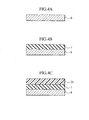
- a first feature of the present invention inheres in a method for manufacturing a surface acoustic wave device, the method comprising: (a) a step of depositing a metal film on a piezo-electric substrate; (b) a step of coating a photosensitive resin film on the metal film; (c) a step of photo-exposing and developing the resin film, forming a photosensitive resin pattern, and selectively exposing a part of the metal film; (d) a step of grounding the metal film using the exposed metal film as a window for grounding; (e) a step of irradiating an electron beam to the piezo-electric substrate, and measuring the resin pattern while the metal film is grounded; (f) a step of etching the metal film using the photosensitive resin pattern as a mask, and forming a metal pattern; and (g) a step of removing the photosensitive resin pattern.
- the metal film on the piezo-electric substrate by grounding the metal film on the piezo-electric substrate, and by measuring the photosensitive resin pattern, electrification on the piezo-electric substrate can be prevented, and therefore the shape of the photosensitive resin pattern can be measured with high reproducibility and high precision.
- a second feature of the present invention inheres in a method for manufacturing a surface acoustic wave device, comprising: (a) a step of depositing a metal film on a piezo-electric substrate; (b) a step of coating a photosensitive resin film on the metal film; (c) a step of exposing and developing the resin film, and forming a resin pattern; (d) a step of etching the metal film using the resin pattern as a mask so as to form a metal pattern; (e) a step of removing the resin pattern; (f) a step of grounding a part of the metal pattern; and (g) a step of irradiating an electron beam to the piezo-electric substrate, and measuring the shape of the metal pattern electrically connected to the grounded part, when the part of the metal pattern is grounded.
- a third feature of the present invention inheres in a tester, comprising: (a) an electron gun for generating an electron beam; (b) a condenser lens for converging the electron beam; (c) an electron beam scanning portion for scanning the electron beam; (d) a detector for detecting secondary electrons generating from a measuring object by scanning of the electron beam; and (e) a grounding tool for connecting ground electrical potential to a metal film as one of a film at the under part of the measuring object, and the measuring object.
- the electronic beam can be irradiated without storing electrons on the piezo-electric substrate.
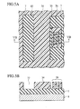
- a tester of a surface acoustic wave device includes an electron gun 1 for generating and irradiating an electron beam to provide primary electrons, a condenser lens 2 for converging the electron beam on the substrate 9, a scanning portion 2 for scanning the electron beam on the substrate 9, a secondary electron detector 4 for detecting second electrons generated from the substrate 9 irradiated by the primary electrons, a substrate holder 5 for holding the substrate 9, and a grounding tool 6.
- the grounding tool 6 is conductive and can be in contact with the metal film 7 on the measuring substrate 9.
- the grounding tool 6 includes a conductive contacting head 12, which can be in contact with the metal film 7, an arm portion 47 attached at the tip of the contacting head 12, and a shaft 48 arranged at the opposite side of the contacting head 12 of the arm portion 47. Furthermore, the tester includes a vacuum chamber 50 accommodating the electron gun 1 and the substrate 9, an picture formation unit 51 for forming a picture based on the detected amount of the secondary electrons from each position on the substrate 9 on which the electron beam was scanned, and a critical dimension measurement unit 52 for detecting the outline of the comb-shaped-electrodes based on the formed picture, and measuring the line-width thereof.
- the substrate 9 has a two-layer structure, which consists of a circular piezo-electric substrate 8 made of lithium tantalate (LiTaO 3 ), and a metal film 7 made of aluminum (Al) formed on the piezo-electric substrate 9.
- Lithium niobate LiNbO 3
- metal patterns for constituting the surface acoustic wave device 11 are formed by the metal film 7 (refer to FIG.2 for details of the metal patterns).
- the metal film 7 is disposed at a position, which can provide contact with the grounding tool 6.
- an opening 10 for contact, formed in the metal part 7, is also arranged at a circumferential part of the substrate 9 which can also contact with the grounding tool 6.
- the grounding tool 6 is arranged in the position 13 beside the substrate 9.
- the grounding tool 6 is movable on the shaft 48 as a center thereof.
- the grounding tool 6 can move to the position 46 where the contacting head 12 can contact the metal film 7, and to the position 14 where the contacting head 12 corresponds with the opening 10.
- the contacting head 12 is also movable so as not to contact with the metal film 7 after measurement.
- the surface acoustic wave device 11 has plural metal patterns consisting of the metal film 7.
- the metal patterns include comb-shaped-electrodes 24 and 27 for input, comb-shaped-electrodes 30 and 33 for output; bonding pads 22, 25, 28, and 31, reflectors 21a and 21b, and ground lines 15 to 20.
- the comb-shaped-electrodes 24, 27, 30, and 33, and the bonding pads 22, 25, 28, and 31 are respectively connected to each other with connection lines 23, 26, 29, and 32.
- the bonding pads 22, 25, 28, and 31, and the metal film 7 on dicing lines are connected with the ground lines 16, 20, 17, and 19.
- the reflectors 21a and 21b, and the metal film 7 on the dicing lines are connected with the ground lines 15 and 18.
- the comb-shaped-electrodes 24, 27, 30, and 33, and the reflectors 21a and 21b, which are electrically connected to the metal film 7 on the circumference region of the substrate 9 through the ground lines, have the same electric potentials.
- the current 38 of electrons is formed when the contacting head 12 of the grounding tool 6 contacts the metal film 7.
- the current 38 of electrons includes: (a) electrons charged on the piezo-electric substrate 8 by temperature change in the manufacturing process; (b) primary electrons irradiated by the electron beam; and (c) electrons further generated on the piezo-electric substrate 8 since the substrate 8 is further polarized by heating caused by the beam irradiation.
- the current 38 runs from the metal film 7 into finally the grounding tool 6 so as to reduce an incline of electrical current potential.
- the current 38 suppress to accumulate electrons on the piezo-electric substrate 8 in resin patterns such as the photosensitive resin pattern 36, which are used as a measurement object and in proximity of the patterns. Consequently, a trajectory of the electron beam 37 is not deflected, and highly precise and reproducible measurements of the shape of photosensitive resin patterns are possible.
- the line-width of the comb-shaped photosensitive resin pattern was respectively measured with the tester according to the embodiment of the present invention and with a conventional line-width-measurement system without the grounding tool 6, and the result was compared.
- a standard deviation value was about 1nm by the measurement method according to the embodiment of the present invention.
- a standard deviation was about 5nm by the conventional measurement method without the grounding tool 6. This demonstrated that highly precise and highly reproducible measurements are possible using the measurement method according to the embodiment of the present invention.
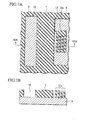
- the current 39 of electrons includes: (a) electrons further charged on the piezo-electric substrate 8 by polarization due to temperature change in the manufacturing process; (b) primary electrons irradiated by the beam; and (c) electrons further charged on the piezo-electric substrate 8 by heating caused by irradiation.
- the flow 39 of electrons runs from the metal film 7 into the grounding tool 6 through the ground line 15 so as to reduce an incline of electrical current potential.
- the flow 39 stops electrons from accumulating in the piezo-electric substrate 8 of the metal film 7, such as the reflector 21a used a measurement object, and in proximity to the object. Accordingly, a trajectory of the electron beam 37 is not deflected, and highly precise and reproducible measurements of the shape of photosensitive resin patterns become possible.
- the line-width of the comb-shaped-electrode which is a metal pattern, was measured with the tester according to the embodiment of the present invention and with the conventional line-width-measurement system without the grounding tool 6 respectively, and compared.
- the standard deviation value was about 1nm by the measurement method according to the embodiment of the present invention.
- the standard deviation was about 5nm by the conventional measurement method without the grounding tool 6. This demonstrated that highly precise and highly reproducible measurements are possible using the measurement method according to the embodiment of the present invention.
- the shape of the reflector can be measured more precisely. This is because, for instance, in a case where the reflector 21a is measured, the reflector 21a, directly connected to the ground line 15, becomes charged less easily than the comb-shaped-electrode 24, which is far from a ground line.
- materials and quantity of material parts are in one of the embodiments of the present invention. Even if other materials replace these materials, technical effectiveness does not change. For example, technical effectiveness does not change when lithium tetraborate (LiB 4 O 7 ) is used as a piezo-electric substrate.
- LiB 4 O 7 lithium tetraborate
- the grounding tool 6 may further include other elements, like a clamp portion (a spring portion) holding the contacting head 12 in the substrate 9, and a drive portion rotating the shaft 48. Furthermore, the grounding tool 6 may further have a portion moving the arm portion 47 from top and bottom and right and left.
- the metal film 7 based on Al is deposited on the piezo-electric substrate 8.
- effectiveness is not changed even in a case where the metal film consisting of materials different from Al is deposited on the piezo-electric substrate 8 and in a case of a multi-layer structure having different laminated materials.
- the type and shape of a photosensitive resin pattern and a metal pattern are not particularly limited, for instance, like comb-shaped patterns.
- the line-width of the photosensitive resin pattern and the line-width of the comb-shaped-electrode of the metal patterns are measured.
- the line-width and the shape are positions, such as the photosensitive resin pattern 35 and the reflector 21a, which are necessary in quality control may be measured and checked.
- the number of times of measurement can be performed is not particularly limited.
Landscapes
- Engineering & Computer Science (AREA)
- Chemical & Material Sciences (AREA)
- Physics & Mathematics (AREA)
- Nanotechnology (AREA)
- Acoustics & Sound (AREA)
- Analytical Chemistry (AREA)
- Crystallography & Structural Chemistry (AREA)
- Manufacturing & Machinery (AREA)
- General Physics & Mathematics (AREA)
- Condensed Matter Physics & Semiconductors (AREA)
- Mathematical Physics (AREA)
- Theoretical Computer Science (AREA)
- Surface Acoustic Wave Elements And Circuit Networks Thereof (AREA)
Abstract
Description
Claims (17)
- A method for manufacturing a surface acoustic wave device, comprising:a step of depositing a metal film on a piezo-electric substrate;a step of coating a photosensitive resin film on the metal film;a step of exposing and developing the photosensitive resin film, and forming a photosensitive resin pattern, and selectively exposing a part of the metal film;a step of grounding the metal film using the exposed metal film as a window for grounding;a step of irradiating an electron beam to the piezo-electric substrate, and measuring the photosensitive resin pattern when the metal film is grounded;a step of etching the metal film using the photosensitive resin pattern as a mask, and forming a metal pattern; anda step of removing the photosensitive resin pattern.
- The method according to claim 1, wherein the line-width of the resin pattern is less than 2.0 µm and more than 0.35 µm.
- The method according to claim 1, wherein the piezo-electric substrate consists of one of lithium tantalate (LiTaO3), and lithium niobate (LiNbO3).
- The method according to claim 1, wherein the metal film is grounded by contacting a contacting head of a grounding tool with the exposed metal film.
- The method according to claim 1, wherein whether the measured photosensitive resin pattern is within a range of specifications is determined after the step of measuring the shape of the photosensitive resin pattern.
- The method according to claim 4, further comprising:a step of grounding the metal film electrically connected to the metal pattern by contacting the contacting head of the grounding tool with the metal film, after the step of removing the resin pattern; and,a step of irradiating the electron beam to the piezo-electric substrate, and measuring the shape of the metal pattern when the metal film is grounded.
- A method for manufacturing a surface acoustic wave device, comprising:a step of depositing a metal film on a piezo-electric substrate;a step of coating a photosensitive resin film on the metal film;a step of exposing and developing the photosensitive resin film, and forming a resin pattern;a step of etching the metal film using the photosensitive resin pattern as a mask so as to form a metal pattern;a step of removing the photosensitive resin pattern;a step of grounding a part of the metal pattern; anda step of irradiating an electron beam to the piezo-electric substrate, and measuring the shape of the metal pattern electrically connected to the grounded part, when the part of the metal pattern is grounded.
- The method according to claim 7, wherein the line-width of the metal pattern is less than 2.0 µm and more than 0.35 µm.
- The method according to claim 7, wherein the piezo-electric substrate consists of one of lithium tantalate (LiTaO3), and lithium niobate (LiNbO3).
- The method according to claim 7, wherein whether the shape of the measured metal pattern is within the range of specifications is determined, after the step of measuring the shape of the metal pattern.
- The method according to claim 7, wherein the metal patterns, used as a shape measurement object, are patterns of a reflector.
- A tester, comprising:an electron gun generating an electron beam;a condenser lens converging the electron beam;an electron beam scanning portion for scanning the electron beam;a detector detecting secondary electrons generated from a measuring object by scanning of the electron beam; anda grounding tool connecting ground electrical current potential of a metal film as one of a film at a under part of the measuring object, and the measuring object.
- The tester according to claim 12, wherein the grounding tool comprises:a contacting head configured to contact the grounding tool with the metal film;an arm portion arranged at one end of the contacting head;a shaft arranged at the other end of the contacting head, and configured to rotate the arm portion.
- The tester according to claim 13, further comprising a holder holding a sample provided the metal film.
- The tester in scope of claim 13, further comprising a vacuum chamber configured to receive the electron gun and the measuring object therein.
- The tester according to claim 13, further comprising a picture formation unit forming a picture based on amounts of the detected secondary electrons.
- A tester according to claim 16, further comprising a critical dimension measurement unit measuring the shape of the measuring object based on the picture formed by the picture formation unit.
Applications Claiming Priority (3)
| Application Number | Priority Date | Filing Date | Title |
|---|---|---|---|
| JP2001017507 | 2001-01-25 | ||
| JP2001017507 | 2001-01-25 | ||
| PCT/JP2001/008639 WO2002060054A1 (en) | 2001-01-25 | 2001-10-01 | Method for manufacturing surface acoustic wave device and inspecting instrument |
Publications (2)
| Publication Number | Publication Date |
|---|---|
| EP1363395A1 true EP1363395A1 (en) | 2003-11-19 |
| EP1363395A4 EP1363395A4 (en) | 2009-09-02 |
Family
ID=18883707
Family Applications (1)
| Application Number | Title | Priority Date | Filing Date |
|---|---|---|---|
| EP01970317A Ceased EP1363395A4 (en) | 2001-01-25 | 2001-10-01 | Method for manufacturing surface acoustic wave device and inspecting instrument |
Country Status (5)
| Country | Link |
|---|---|
| US (1) | US7029828B2 (en) |
| EP (1) | EP1363395A4 (en) |
| JP (1) | JP4043949B2 (en) |
| CN (1) | CN1278486C (en) |
| WO (1) | WO2002060054A1 (en) |
Cited By (1)
| Publication number | Priority date | Publication date | Assignee | Title |
|---|---|---|---|---|
| WO2021083773A1 (en) * | 2019-10-28 | 2021-05-06 | Asml Netherlands B.V. | System for inspecting and grounding a mask in a charged particle system |
Families Citing this family (2)
| Publication number | Priority date | Publication date | Assignee | Title |
|---|---|---|---|---|
| JP4675697B2 (en) * | 2005-07-06 | 2011-04-27 | 株式会社東芝 | Mask pattern inspection method, exposure condition verification method, and semiconductor device manufacturing method |
| CN104333341B (en) * | 2014-11-14 | 2018-01-09 | 中国电子科技集团公司第二十六研究所 | SAW device resists 300 DEG C of high temperature stripping means |
Family Cites Families (7)
| Publication number | Priority date | Publication date | Assignee | Title |
|---|---|---|---|---|
| US5106471A (en) * | 1990-04-02 | 1992-04-21 | Motorola, Inc. | Reactive ion etch process for surface acoustic wave (SAW) device fabrication |
| JPH03293808A (en) * | 1990-04-11 | 1991-12-25 | Fujitsu Ltd | Production of surface acoustic wave element |
| JP2927627B2 (en) * | 1992-10-20 | 1999-07-28 | 株式会社日立製作所 | Scanning electron microscope |
| JP3184675B2 (en) * | 1993-09-22 | 2001-07-09 | 株式会社東芝 | Measuring device for fine patterns |
| JPH11298284A (en) * | 1998-04-13 | 1999-10-29 | Toshiba Corp | Surface acoustic wave device |
| JPH11338147A (en) * | 1998-05-21 | 1999-12-10 | Toshiba Corp | Method for manufacturing semiconductor device |
| JP2000173525A (en) * | 1998-12-03 | 2000-06-23 | Hitachi Ltd | Sample charge removal device |
-
2001
- 2001-10-01 CN CNB018222609A patent/CN1278486C/en not_active Expired - Fee Related
- 2001-10-01 JP JP2002560272A patent/JP4043949B2/en not_active Expired - Fee Related
- 2001-10-01 EP EP01970317A patent/EP1363395A4/en not_active Ceased
- 2001-10-01 WO PCT/JP2001/008639 patent/WO2002060054A1/en not_active Ceased
- 2001-10-01 US US10/466,546 patent/US7029828B2/en not_active Expired - Lifetime
Cited By (3)
| Publication number | Priority date | Publication date | Assignee | Title |
|---|---|---|---|---|
| WO2021083773A1 (en) * | 2019-10-28 | 2021-05-06 | Asml Netherlands B.V. | System for inspecting and grounding a mask in a charged particle system |
| CN115298792A (en) * | 2019-10-28 | 2022-11-04 | Asml荷兰有限公司 | System for inspecting and grounding a mask in a charged particle system |
| US12142451B2 (en) | 2019-10-28 | 2024-11-12 | Asml Netherlands B.V. | System for inspecting and grounding a mask in a charged particle system |
Also Published As
| Publication number | Publication date |
|---|---|
| US7029828B2 (en) | 2006-04-18 |
| JP4043949B2 (en) | 2008-02-06 |
| EP1363395A4 (en) | 2009-09-02 |
| CN1488191A (en) | 2004-04-07 |
| WO2002060054A1 (en) | 2002-08-01 |
| US20040047982A1 (en) | 2004-03-11 |
| JPWO2002060054A1 (en) | 2004-05-27 |
| CN1278486C (en) | 2006-10-04 |
Similar Documents
| Publication | Publication Date | Title |
|---|---|---|
| JP5644850B2 (en) | Electron beam adjustment method, charged particle optical system controller, and scanning electron microscope | |
| US8026482B2 (en) | Charged particle beam apparatus and control method therefor | |
| WO2011001586A1 (en) | Charged particle beam apparatus and method for stably obtaining charged particle beam image | |
| JP2902612B2 (en) | Sample for transmission electron microscope analysis and method for producing the same | |
| TW201907438A (en) | Device using multiple charged particle beams | |
| US5912468A (en) | Charged particle beam exposure system | |
| TW200820321A (en) | Electron beam dimension measuring device and electron beam dimension measuring method | |
| JPS60201625A (en) | Method and device for inspecting error of exposure mask | |
| US7029828B2 (en) | Method for manufacturing surface acoustic wave device and inspecting instrument | |
| JP4305421B2 (en) | Electron beam adjustment method, charged particle optical system controller, and scanning electron microscope | |
| JPS63231858A (en) | electron beam device | |
| JP2002158167A (en) | Exposure method and exposure apparatus | |
| JP4506588B2 (en) | Charged particle beam irradiation method and charged particle beam apparatus | |
| JP3353051B2 (en) | Line width measurement of integrated circuit structures | |
| US7560693B2 (en) | Electron-beam size measuring apparatus and size measuring method with electron beams | |
| US4983864A (en) | Electronic beam drawing apparatus | |
| JP2025522268A (en) | Charged particle beam device with high speed focus correction function and method thereof | |
| JPH01221637A (en) | Observed sample processing method | |
| JP4477435B2 (en) | Deflector manufacturing method, charged particle beam exposure apparatus, and device manufacturing method | |
| JP2003077413A (en) | Electron beam apparatus and semiconductor device manufacturing method using the same | |
| JP2834243B2 (en) | Antistatic method in electron beam lithography | |
| CN115298792A (en) | System for inspecting and grounding a mask in a charged particle system | |
| WO2019063558A1 (en) | Image contrast enhancement in sample inspection | |
| JPH1013178A (en) | Method for manufacturing surface acoustic wave device | |
| KR100217336B1 (en) | Antistatic Method of Semiconductor Analytical Sample |
Legal Events
| Date | Code | Title | Description |
|---|---|---|---|
| PUAI | Public reference made under article 153(3) epc to a published international application that has entered the european phase |
Free format text: ORIGINAL CODE: 0009012 |
|
| 17P | Request for examination filed |
Effective date: 20030812 |
|
| AK | Designated contracting states |
Kind code of ref document: A1 Designated state(s): DE FR GB |
|
| A4 | Supplementary search report drawn up and despatched |
Effective date: 20090803 |
|
| RIC1 | Information provided on ipc code assigned before grant |
Ipc: H01L 21/027 20060101ALI20090728BHEP Ipc: H03H 9/02 20060101ALI20090728BHEP Ipc: H03H 3/08 20060101AFI20020809BHEP Ipc: H01J 37/28 20060101ALI20090728BHEP |
|
| 17Q | First examination report despatched |
Effective date: 20091113 |
|
| STAA | Information on the status of an ep patent application or granted ep patent |
Free format text: STATUS: THE APPLICATION HAS BEEN REFUSED |
|
| 18R | Application refused |
Effective date: 20110107 |