EP1363366A1 - Procedé de stabilisation pour source laser à reflecteur distribué - Google Patents
Procedé de stabilisation pour source laser à reflecteur distribué Download PDFInfo
- Publication number
- EP1363366A1 EP1363366A1 EP03290929A EP03290929A EP1363366A1 EP 1363366 A1 EP1363366 A1 EP 1363366A1 EP 03290929 A EP03290929 A EP 03290929A EP 03290929 A EP03290929 A EP 03290929A EP 1363366 A1 EP1363366 A1 EP 1363366A1
- Authority
- EP
- European Patent Office
- Prior art keywords
- wavelength
- section
- laser
- current
- value
- Prior art date
- Legal status (The legal status is an assumption and is not a legal conclusion. Google has not performed a legal analysis and makes no representation as to the accuracy of the status listed.)
- Granted
Links
- 238000000034 method Methods 0.000 title claims abstract description 15
- 230000006641 stabilisation Effects 0.000 title description 2
- 230000003287 optical effect Effects 0.000 claims abstract description 15
- 230000010355 oscillation Effects 0.000 claims description 14
- 238000005259 measurement Methods 0.000 claims description 10
- 238000002310 reflectometry Methods 0.000 claims description 9
- 238000002347 injection Methods 0.000 claims description 5
- 239000007924 injection Substances 0.000 claims description 5
- 230000000737 periodic effect Effects 0.000 claims description 5
- 239000004065 semiconductor Substances 0.000 claims description 5
- 230000000087 stabilizing effect Effects 0.000 claims description 2
- 230000005540 biological transmission Effects 0.000 abstract description 5
- 239000000243 solution Substances 0.000 description 8
- 230000006870 function Effects 0.000 description 7
- 230000000694 effects Effects 0.000 description 4
- 230000007423 decrease Effects 0.000 description 3
- 230000003667 anti-reflective effect Effects 0.000 description 2
- 238000006243 chemical reaction Methods 0.000 description 2
- 238000005253 cladding Methods 0.000 description 2
- 239000000463 material Substances 0.000 description 2
- 230000032683 aging Effects 0.000 description 1
- 230000003321 amplification Effects 0.000 description 1
- 230000015572 biosynthetic process Effects 0.000 description 1
- 239000000969 carrier Substances 0.000 description 1
- 230000015556 catabolic process Effects 0.000 description 1
- 230000008859 change Effects 0.000 description 1
- 239000000470 constituent Substances 0.000 description 1
- 230000008878 coupling Effects 0.000 description 1
- 238000010168 coupling process Methods 0.000 description 1
- 238000005859 coupling reaction Methods 0.000 description 1
- 230000003247 decreasing effect Effects 0.000 description 1
- 238000006731 degradation reaction Methods 0.000 description 1
- 238000001514 detection method Methods 0.000 description 1
- 238000000295 emission spectrum Methods 0.000 description 1
- 230000001747 exhibiting effect Effects 0.000 description 1
- 238000000691 measurement method Methods 0.000 description 1
- 238000003199 nucleic acid amplification method Methods 0.000 description 1
- 230000003071 parasitic effect Effects 0.000 description 1
- 239000004038 photonic crystal Substances 0.000 description 1
- 238000005036 potential barrier Methods 0.000 description 1
- 230000004044 response Effects 0.000 description 1
- 150000003839 salts Chemical class 0.000 description 1
- 238000001228 spectrum Methods 0.000 description 1
- 238000011105 stabilization Methods 0.000 description 1
- 230000001629 suppression Effects 0.000 description 1
- 239000012780 transparent material Substances 0.000 description 1
- VLCQZHSMCYCDJL-UHFFFAOYSA-N tribenuron methyl Chemical compound COC(=O)C1=CC=CC=C1S(=O)(=O)NC(=O)N(C)C1=NC(C)=NC(OC)=N1 VLCQZHSMCYCDJL-UHFFFAOYSA-N 0.000 description 1
Images


Classifications
-
- H—ELECTRICITY
- H01—ELECTRIC ELEMENTS
- H01S—DEVICES USING THE PROCESS OF LIGHT AMPLIFICATION BY STIMULATED EMISSION OF RADIATION [LASER] TO AMPLIFY OR GENERATE LIGHT; DEVICES USING STIMULATED EMISSION OF ELECTROMAGNETIC RADIATION IN WAVE RANGES OTHER THAN OPTICAL
- H01S5/00—Semiconductor lasers
- H01S5/06—Arrangements for controlling the laser output parameters, e.g. by operating on the active medium
- H01S5/062—Arrangements for controlling the laser output parameters, e.g. by operating on the active medium by varying the potential of the electrodes
- H01S5/0625—Arrangements for controlling the laser output parameters, e.g. by operating on the active medium by varying the potential of the electrodes in multi-section lasers
- H01S5/06255—Controlling the frequency of the radiation
- H01S5/06256—Controlling the frequency of the radiation with DBR-structure
-
- H—ELECTRICITY
- H01—ELECTRIC ELEMENTS
- H01S—DEVICES USING THE PROCESS OF LIGHT AMPLIFICATION BY STIMULATED EMISSION OF RADIATION [LASER] TO AMPLIFY OR GENERATE LIGHT; DEVICES USING STIMULATED EMISSION OF ELECTROMAGNETIC RADIATION IN WAVE RANGES OTHER THAN OPTICAL
- H01S5/00—Semiconductor lasers
- H01S5/06—Arrangements for controlling the laser output parameters, e.g. by operating on the active medium
- H01S5/0617—Arrangements for controlling the laser output parameters, e.g. by operating on the active medium using memorised or pre-programmed laser characteristics
-
- H—ELECTRICITY
- H01—ELECTRIC ELEMENTS
- H01S—DEVICES USING THE PROCESS OF LIGHT AMPLIFICATION BY STIMULATED EMISSION OF RADIATION [LASER] TO AMPLIFY OR GENERATE LIGHT; DEVICES USING STIMULATED EMISSION OF ELECTROMAGNETIC RADIATION IN WAVE RANGES OTHER THAN OPTICAL
- H01S5/00—Semiconductor lasers
- H01S5/06—Arrangements for controlling the laser output parameters, e.g. by operating on the active medium
- H01S5/068—Stabilisation of laser output parameters
- H01S5/0683—Stabilisation of laser output parameters by monitoring the optical output parameters
- H01S5/0687—Stabilising the frequency of the laser
Definitions
- the invention lies in the field of sources emission of laser waves intended in particular for optical telecommunications. It concerns more particularly tunable sources wavelength using distributed reflector lasers, commonly called DBR lasers (from the English “Distributed Bragg Reflector ").
- DBR lasers from the English “Distributed Bragg Reflector ").
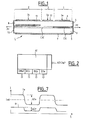
- DBR laser An example of a DBR laser is shown schematically in Figure 1. It's a semiconductor component monolithic typically composed of a section amplifier 1, called “active”, coupled to a so-called section “Bragg” 2. Optionally, a section called “phase” 3 can be arranged between the active and Bragg sections.
- the active section has a vertical structure conventionally constituted of an active amplifying layer CA disposed between two layers of sheath 4, 5 of doping opposed.
- This active layer CA is usually composed of a succession of quantum wells separated by layers forming potential barriers.
- Upper electrodes 6 and lower 7 allow a current injection Ia to through these layers so as to produce an effect optical amplification.
- the Bragg section 2 is a reflective section having a maximum reflectivity for at least one reflection wavelength value. One of its ends is thus coupled to the active section 1. It has a vertical structure consisting of a guide layer CA 'homogeneous (called “bulk” or “bulk” in English) disposed between two layers of sheath.
- a network 8 is located in one of the cladding layers in the vicinity of the guiding layer and forms along the guide a periodic alternation of materials of different indices.
- This network 8 is designed to constitute a wavelength selective reflector having at least one main peak of reflectivity, that is to say a wavelength of maximum reflection.
- the outer face 9 of the active section 1 constitutes a non-selective wavelength reflector and forms with the Bragg section 2 a resonant cavity of Fabry-Perot containing the active section 1.
- the laser power created in the cavity is extracted essentially by this external face 9 which is then called “front face”.
- She is made semi-reflective by means of an anti-reflective layer appropriate.
- its reflectivity is of the order of 1.5 to 5% to allow both laser oscillation and an emission outside the component of the laser wave created.
- the end of the Bragg section that is not coupled to the active section constitutes a second face external 10 of the component, called “back face”, and to avoid the formation of parasitic modes, this one is rendered strongly anti-reflective.
- the laser power created in the cavity can be extracted essentially by the end of the Bragg section that is not coupled to the active section. This end then becomes a face before or is coupled with other sections embedded in component, such as photodetector, amplifier, modulator.
- the outer face 9 of the section active 1 becomes a back face that can be strongly reflective, typically with superior reflectivity at 90%.
- the laser oscillation is possible for a set of longitudinal resonant modes (Fabry-Perot modes) whose wavelengths are imposed by the optical length of the cavity. An oscillation will occur in one of these modes if there is sufficient agreement between its wavelength and the Bragg wavelength ⁇ B.
- Fabry-Perot modes longitudinal resonant modes
- the guiding layer CA 'of the Bragg section must be composed of a transparent material over the entire range of operating wavelengths and have an effective index nb that can vary according to a control.
- the material is for example an active medium chosen so that its index depends on the density of carriers it contains.
- the guiding layer CA ' is then disposed between the two cladding layers 4, 5 of opposite dopings and the Bragg section comprises an upper electrode 11 cooperating with the aforementioned lower electrode 7 to allow an injection of an electric control current Ib in the guiding layer CA '.
- a finer adjustment of the wavelength oscillation can also be achieved by a the temperature of the component.
- the temperature of the component By acting on the temperature, we can adjust the indices of the layers guiding the cavity and thus its optical length, which has effect of shifting the comb of wavelengths Fabry-Perot modes.
- phase section 3 extends the Bragg section towards the active section 1, with an identical vertical structure but where the Bragg grating is absent. It also comprises an upper electrode 12 cooperating with the lower electrode 7 of the component to allow an injection of electric current Ip in the guiding layer CA '.
- the optical length of the cavity is modified, which shifts the wavelength comb of the Fabry-Perot modes without influencing the Bragg wavelength ⁇ B.
- a tunable laser of a type described above will therefore be determined by three parameters: the current Ia injected into the active section 1, the current Ib injected into the Bragg section 2 and the current Ip injected into the phase 3 section, or if there is no section phase, the temperature.
- a power laser emission is imposed fixed and selectable wavelength among a grid standardized (ITU grid).
- ITU grid standardized
- this table can then cooperate with an electronic circuit who drives the component, circuit assembly electronic and component in the form of a module thus constituting an autonomous functional unit.
- SMSR Segment Mode Suppression Ratio
- the preceding provisions do not make it possible to provide an automatic control of the SMSR. It is therefore necessary to provide another slaving which accurately adjusts the Bragg wavelength ⁇ B according to a measurement of the SMSR, so as to make it maximum, or at least at least equal to the imposed value.
- servocontrol using a direct measurement of the SMSR by means of an optical spectrum analyzer is not conceivable because such a device is impossible in practice to integrate into a laser emission module. It is therefore preferable to look for an indirect measurement of the SMSR using another parameter that can be used to maximize the SMSR, but easier to measure.
- the problem that the invention aims to solve is to achieve a servo such as, for each length selected waveform and even with high transmission power, the laser is stably maintained away from operation corresponding to mode jumps.
- the enslavement must be able to stabilize the SMSR at its maximum value or at least the closest of it.
- Figures 3 to 5 will illustrate the phenomena observed in the case of a particular component of conventional type made of InP.
- FIG. 3 shows a curve representative of the variations of the wavelength ⁇ of the main oscillating mode of the cavity as a function of the current Ib (expressed in mA) injected into the Bragg section.
- the Bragg wavelength ⁇ B being a decreasing function of this current Ib, it is verified that the wavelength ⁇ decreases when Ib increases.
- mode jumps are manifested by discontinuities in the curve.
- Each selectable wavelength ⁇ 1 , ⁇ 2 , ..., ⁇ q , for example ⁇ q lies between two consecutive Bragg wavelength values, for example ⁇ B 1, ⁇ B 2, which correspond to respectively to mode jumps, which correspond on the curve to particular values, for example Ib1 and Ib2, of the Bragg current Ib.
- the Mode jumps occur when Ib is 10 or 11.5 mA.
- FIG. 4 shows a curve representative of the variations of the SMSR (expressed in dB) as a function of the current Ib. For each selectable wavelength ⁇ 1 , ⁇ 2 , ..., ⁇ q , very rapid decreases in the SMSR are observed. in the vicinity of the values of the Bragg current that correspond to the mode jumps. Furthermore, it is noted that the SMSR is generally maximum for the values of Ib located substantially between two consecutive values of Ib corresponding to mode jumps. However, the SMSR can also be maximum for Ib values different to those located substantially between two consecutive values of Ib corresponding to mode jumps.
- Figure 5 finally shows a representative curve of variations as a function of the current Ib of the derivative dPr / dIa of power Pr emitted by the rear face with respect to current Ia injected into the active section.
- the absolute value of this derivative dPr / dIa is all the more high that the laser has a functioning close to a jump of fashion.
- the set value to be adopted is not necessarily very precise.
- the choice for this value will mainly degrade characteristics of the component, the range of selectable wavelengths and especially the minimum value of the SMSR that we set our.
- the reference value Ref may be a single value common to all the selectable wavelengths ⁇ 1 , ⁇ 2 , ⁇ q .
- each selectable wavelength ⁇ 1 , ⁇ 2 , ⁇ q is associated with a specific reference value Ref.
- the set value Ref0 can be chosen as the set value for each selectable wavelength.
- any selectable wavelength ⁇ 1 , ⁇ 2 , ⁇ q is between two values of consecutive reflection wavelengths ⁇ B 1, ⁇ B 2 which respectively correspond to mode jumps for consecutive values Ib1 and Ib2 of the current Ib, but sometimes the maximum SMSR can be obtained for values of the current Ib, so for reflection wavelengths, neighboring values that cause mode jumps.
- choosing Ref0 as a set value presents the risk of being placed at operating points that are unstable or not very tolerant to drifts or fluctuations of certain parameters.
- said setpoint value is that Refm for which the reflection wavelength ⁇ B is substantially equal to the average ⁇ m of the length values d consecutive reflection wave ⁇ B 1, ⁇ B 2 which respectively correspond to mode jumps.
- the dPr / dIa derivative of the laser power relative to the current Ia injected into the section amplifier requires an assessment of this laser power. This assessment should also be simple as possible to achieve with the type of laser chosen. In practice, laser power can be easily evaluated by measuring the optical power resulting from the second end 10 of the reflective section 2, either in measuring the optical power from the second reflector 9.
- said source comprises servo-control means designed to adjust said reflection wavelength ⁇ B so that for each selected wavelength ⁇ q , the derivative dPr / dIa of said laser power relative to the current Ia injected into the amplifying section 1 is equal to a set value Ref for which said source has a secondary modes SMSR rejection rate close to the maximum value that this rate can take for said selected wavelength ⁇ q .
- the laser emission source comprises first and second adjustable current sources arranged for injecting first and second currents Ia, Ib respectively in said amplifying section 1 and in said reflective section 2.
- the electronic circuit comprises a control unit for controlling these adjustable current sources according to a set point data representative of said selected wavelength ⁇ q and a measurement of said dPr / dIa derivative of laser power.
- the control unit is further provided with a digital processing unit cooperating with an allocation table comprising data representative of reference values Ref associated respectively with said selectable wavelengths ⁇ 1 , ⁇ 2 , ⁇ q .
- FIG. 6 shows a particular embodiment a laser emission source according to the invention.
- the source has a laser component L of the first type previously mentioned, associated with an electronic circuit consisting of a CU control unit, current sources Adjustable Sa, Sb and Sp and a detection device of WL power coupled to the back side of the L component.
- amplifying section 1, reflective 2 and phase 3 of the laser are respectively connected to the sources Sa, Sb and Sp arranged to inject into these sections respectively the currents Ia, Ib and Ip.
- the laser source is designed to automatically stall the laser oscillation on normalized wavelengths. That's why the WL power sensing device includes a first PD photodetector receiving directly part of the rear power Pr and a second photodetector PD ' receiving another part of that power by through a periodic standard filter FP, by example of type Fabry-Pérot, granted on the lengths standardized waveforms selected.
- a periodic standard filter FP by example of type Fabry-Pérot
- the control unit CU is provided to control the adjustable current sources Sa, Sb and Sp according to the principles already explained at the beginning of the description.
- it comprises a processing unit digital PU (for example based on a microcontroller programmable type of conventional).
- the PU processing accesses digital data representative of a set SEL of selected wavelength and Ir and If currents delivered by the photodetectors PD and PD '.
- the PU processing unit generates values of set currents Ia, Ib, Ip as the current sources Sa, Sb, Sp must provide. After digital-to-analog conversion, corresponding command signals are applied to adjustable current sources Sa, Sb and Sp at means of appropriate output interfaces IFa, IFb, IFp.
- the set values of currents Ia, Ib, Ip are determined by the PU unit thanks to the AT allocation table (already mentioned with reference to Figure 2) contained in a memory addressable by the PU unit. So, depending on the SEL setpoint of the wavelength to be selected, the PU unit provides the AD address to the memory and seizes a set of parameter values DIa, DIb, DIp representative of initial setpoint values of currents Ia, Ib, Ip to apply. These initial values are then adjusted by the servo algorithms provided in the PU unit.
- the parameter DIa constitutes the setpoint of current Ia.
- the DIb parameter constitute the initial set value of Ib which sets the Bragg wavelength and therefore selects among the modes oscillating cavity one that has a length wave near the wavelength indicated by the instruction SALT.
- the DIp parameter constitutes the set value initials of Ip, but the effective setpoint is adjusted to maximize the If / Ir ratio of Ir and If currents issued respectively by photodetectors PD and PD ', and so stall the oscillation laser on one of the normalized wavelengths.
- the allocation table AT has an additional field at each address assigned to a DRef parameter (see Figure 2).
- the values of parameter DRef are data representative of values reference set Ref of the derivative dPr / dIa, associated respectively at selectable wavelengths.
- the CU control unit must implement a method for measuring the dPr / dIa derivative of the power laser compared to the current Ia injected into the section Amplifier 1.
- the proposed method consists of modulating periodically the current Ia around a constant value Ia0 (corresponding to the value of parameter DIa provided by the table AT), this modulation having an amplitude predetermined, and to measure the amplitude of modulation periodical of the laser power that results.
- Figure 7 shows the variations as a function of time respectively of current Ia injected into the active section and the current Ir issued by the photodetector PD.
- the measurement of the constituent current Ir a measure of the laser power and the amplitude of modulation ⁇ Ia of the current Ia being constant and known, the modulation amplitude ⁇ Ir of the current Ir will thus constitute a measure of the derivative dPr / dIa.
- the control unit CU is then provided to control the current source Sa so as to periodically modulate the current Ia around the constant value Ia0.
- the modulation rate can be easily developed from the clock signal CK received by the PU unit.
- the modulation has a predetermined amplitude ⁇ Ia and the values of the parameter DRef provided by the table AT (which are the data representative of the reference values Ref) will therefore be reference values of modulation amplitude of the laser power.
- the control unit CU is finally designed to evaluate the periodic modulation amplitude of the laser power, compare it with that of the reference values which is associated with the selected wavelength ⁇ q and, depending on this comparison, reevaluate the control applied to the adjustable current source Sb.
- the amplitude of modulation ⁇ Ia of the current Ia is small compared to its value average Ia0, for example less than 2% of Ia0.
- frequency of this modulation must be much lower than clock frequencies of the transmitted signals.
- the invention is not limited to the embodiment which has just been described. It can use various types of DB laser components and instead of having the PD detector to measure the rear power Pr, we could the have to measure the power before Pf.
- the reflective section 2 described as a conventional Bragg reflector section could have a sampled Bragg reflector, or could be replaced by an equivalent structure such as a photonic crystal section.
Landscapes
- Physics & Mathematics (AREA)
- Condensed Matter Physics & Semiconductors (AREA)
- General Physics & Mathematics (AREA)
- Electromagnetism (AREA)
- Optics & Photonics (AREA)
- Semiconductor Lasers (AREA)
- Lasers (AREA)
- Optical Elements Other Than Lenses (AREA)
Abstract
Description
- un composant semi-conducteur L muni d'une section amplificatrice 1 délimitée par un premier et un second réflecteur 2, 9 formant une cavité résonante permettant plusieurs modes oscillants qui déterminent respectivement plusieurs longueurs d'onde sélectionnables λ1, λ2, λq, ledit premier réflecteur étant une section réfléchissante 2 intégrée au composant et présentant un maximum de réflectivité pour au moins une valeur de longueur d'onde de réflexion λB, cette section réfléchissante 2 ayant une première extrémité couplée à ladite section amplificatrice 1 et une seconde extrémité 10, un courant électrique Ia étant injecté dans ladite section amplificatrice 1, ladite section réfléchissante 2 étant commandable de façon à pouvoir régler ladite valeur de longueur d'onde de réflexion λB et ainsi favoriser l'oscillation d'un desdits modes oscillants présentant une longueur d'onde sélectionnée λq, une puissance laser étant alors créée dans la cavité,
- un composant semi-conducteur L muni d'une section amplificatrice 1 délimitée par un premier et un second réflecteur 2, 9 formant une cavité résonante permettant plusieurs modes oscillants qui déterminent respectivement plusieurs longueurs d'onde sélectionnables λ1, λ2, λq, ledit premier réflecteur étant une section réfléchissante 2 intégrée au composant et présentant un maximum de réflectivité pour au moins une valeur de longueur d'onde de réflexion λB, cette section réfléchissante 2 ayant une première extrémité couplée à ladite section amplificatrice 1 et une seconde extrémité 10, ladite section réfléchissante 2 étant commandable électriquement de façon à pouvoir régler ladite valeur de longueur d'onde de réflexion λB,
- un détecteur pour évaluer une puissance laser créée dans la cavité, et
- un circuit électronique pour injecter un courant électrique Ia dans la section amplificatrice 1 et pour commander ladite longueur d'onde de réflexion λB de façon à favoriser l'oscillation d'un desdits modes oscillants présentant une longueur d'onde sélectionnée λq.
- La figure 1 représente schématiquement un composant laser DBR déjà décrit précédemment.
- figure 2 représente schématiquement une table d'allocation déjà décrite précédemment.
- Les figures 3 à 5 représentent des courbes déjà décrites précédemment montrant les variations en fonction du courant Ib injecté dans la section de Bragg respectivement de la longueur d'onde λ du mode oscillant, du SMSR et de la dérivée dPr/dIa de puissance Pr émise par la face arrière par rapport au courant Ia injecté dans la section active.
- La figure 6 représente un exemple de réalisation d'une source d'émission laser accordable en longueur d'onde selon l'invention.
- La figure 7 représente des chronogrammes montrant les variations en fonction du temps respectivement du courant Ia injecté dans la section active et du courant Ir délivré par un photodétecteur de mesure de la puissance Pr.
Claims (12)
- Procédé pour stabiliser le fonctionnement d'une source d'émission laser accordable en longueur d'onde, ladite source comprenant :ce procédé étant caractérisée en ce qu'il consiste à ajuster ladite longueur d'onde de réflexion (λB) de sorte que pour chaque longueur d'onde sélectionnée (λq), la dérivée (dPr/dIa) de ladite puissance laser par rapport au courant (Ia) injecté dans la section amplificatrice (1) soit maintenue égale à une valeur de consigne (Ref) pour laquelle ladite source présente un taux de réjection des modes secondaires (SMSR) voisin de la valeur maximale que ce taux peut prendre pour ladite longueur d'onde sélectionnée (λq).un composant semi-conducteur (L) muni d'une section amplificatrice (1) délimitée par un premier et un second réflecteur (2, 9) formant une cavité résonante permettant plusieurs modes oscillants qui déterminent respectivement plusieurs longueurs d'onde sélectionnables (λ1, λ2, λq), ledit premier réflecteur étant une section réfléchissante (2) intégrée au composant et présentant un maximum de réflectivité pour au moins une valeur de longueur d'onde de réflexion (λB), cette section réfléchissante (2) ayant une première extrémité couplée à ladite section amplificatrice (1) et une seconde extrémité (10), un courant électrique (Ia) étant injecté dans ladite section amplificatrice (1), ladite section réfléchissante (2) étant commandable de façon à pouvoir régler ladite valeur de longueur d'onde de réflexion (λB) et ainsi favoriser l'oscillation d'un desdits modes oscillants présentant une longueur d'onde sélectionnée (λq), une puissance laser étant alors créée dans la cavité,
- Procédé selon la revendication 1, caractérisée en ce que ladite valeur de consigne (Ref) est une valeur unique commune à toutes les longueurs d'onde sélectionnables (λ1, λ2, λq).
- Procédé selon la revendication 1, caractérisée en ce que chaque longueur d'onde sélectionnable (λ1, λ2, λq) est associée à une valeur de consigne (Ref) spécifique.
- Procédé selon la revendication 2, caractérisée en ce que toute longueur d'onde sélectionnable (λ1, λ2, λq) étant comprise entre deux valeurs de longueurs d'onde de réflexion consécutives (λB1, λB2) qui correspondent respectivement à des sauts de mode, ladite valeur de consigne (Ref) a une valeur voisine de celle (Refm) pour laquelle la longueur d'onde de réflexion (λB) est sensiblement égale à la moyenne (λm) desdites valeurs de longueurs d'onde de réflexion consécutives (λB1, λB2).
- Procédé selon l'une des revendications 1 à 4, caractérisée en ce que pour mesurer ladite dérivée (dPr/dIa) de ladite puissance laser par rapport au courant (Ia) injecté dans la section amplificatrice (1), on module périodiquement ledit courant (Ia) autour d'une valeur constante (Ia0), ladite modulation ayant une amplitude prédéterminée, et on mesure l'amplitude de modulation périodique de ladite puissance laser.
- Procédé selon l'une des revendications 1 à 5, caractérisée en ce que ladite puissance laser est évaluée en mesurant la puissance optique issue de ladite seconde extrémité (10) de la section réfléchissante (2).
- Procédé selon l'une des revendications 1 à 5, caractérisée en ce que ladite puissance laser est évaluée en mesurant la puissance optique issue dudit second réflecteur (9).
- Source d'émission laser accordable en longueur d'onde, comprenant :ladite source étant caractérisée en ce qu'elle comporte des moyens d'asservissement (WL, CU, Sa, Sb) conçus pour ajuster ladite longueur d'onde de réflexion (λB) de sorte que pour chaque longueur d'onde sélectionnée (λq), la dérivée (dPr/dIa) de ladite puissance laser par rapport au courant (Ia) injecté dans la section amplificatrice (1) soit égale à une valeur de consigne (Ref) pour laquelle ladite source présente un taux de réjection des modes secondaires (SMSR) voisin de la valeur maximale que ce taux peut prendre pour ladite longueur d'onde sélectionnée (λq).un composant semi-conducteur (L) muni d'une section amplificatrice (1) délimitée par un premier et un second réflecteur (2, 9) formant une cavité résonante permettant plusieurs modes oscillants qui déterminent respectivement plusieurs longueurs d'onde sélectionnables (λ1, λ2, λq), ledit premier réflecteur étant une section réfléchissante (2) intégrée au composant et présentant un maximum de réflectivité pour au moins une valeur de longueur d'onde de réflexion (λB), cette section réfléchissante (2) ayant une première extrémité couplée à ladite section amplificatrice (1) et une seconde extrémité (10), ladite section réfléchissante (2) étant commandable électriquement de façon à pouvoir régler ladite valeur de longueur d'onde de réflexion (λB),un détecteur (PD) pour évaluer une puissance laser créée dans la cavité, etun circuit électronique (CU, Sa, Sb) pour injecter un courant électrique (Ia) dans la section amplificatrice (1) et pour commander ladite longueur d'onde de réflexion (λB) de façon à favoriser l'oscillation d'un desdits modes oscillants présentant une longueur d'onde sélectionnée (λq),
- Source d'émission laser selon la revendication 8, caractérisée en ce que ladite section réfléchissante (2) étant commandable par injection de courant électrique (Ib), ladite source d'émission laser comporte des première et seconde sources de courant ajustables (Sa, Sb) disposées pour injecter des premier et de second courants (la, Ib) respectivement dans ladite section amplificatrice (1) et dans ladite section réfléchissante (2), en ce que ledit circuit électronique (CU, Sa, Sb) comprend une unité de commande (CU) pour commander lesdites sources de courant ajustables (Sa, Sb) en fonction d'une donnée de consigne (SEL) représentative de ladite longueur d'onde sélectionnée (λq) et d'une mesure de ladite dérivée (dPr/dIa) de puissance laser, et en ce que ladite unité de commande (CU) est munie d'une unité de traitement numérique (PU) coopérant avec une table d'allocation (AT) comportant des données (DRef) représentatives de valeurs de consigne (Ref) associées respectivement auxdites longueurs d'onde sélectionnables (λ1, λ2, λq).
- Source d'émission laser selon la revendication 9, caractérisée en ce que ladite unité de commande (CU) est prévue pour commander ladite première source de courant (Sa) de façon moduler périodiquement ledit premier courant (Ia) autour d'une valeur constante (Ia0), ladite modulation ayant une amplitude (ΔIa) prédéterminée, lesdites données (DRef) représentatives desdites valeurs de consigne (Ref) étant des valeurs de référence d'amplitude de modulation de puissance laser, en ce que l'unité de commande (CU) est prévue pour évaluer l'amplitude de modulation périodique de ladite puissance laser, la comparer à celle desdites valeurs de référence qui est associée à ladite longueur d'onde sélectionnée (λq) et, en fonction de cette comparaison, réévaluer la commande appliquée à ladite seconde sources de courant ajustables (Sb).
- Source d'émission laser selon l'une des revendications 8 à 10, caractérisée en ce que ledit détecteur (PD) est disposé pour mesurer la puissance optique (Pr) issue de ladite seconde extrémité (10) de la section réfléchissante (2).
- Source d'émission laser selon l'une des revendications 8 à 10, caractérisée en ce que ledit détecteur (PD) est disposé pour mesurer la puissance optique (Pf) issue dudit second réflecteur (9).
Applications Claiming Priority (2)
| Application Number | Priority Date | Filing Date | Title |
|---|---|---|---|
| FR0204868 | 2002-04-18 | ||
| FR0204868A FR2838877B1 (fr) | 2002-04-18 | 2002-04-18 | Procede de stabilisation pour source laser a reflecteur distribue |
Publications (2)
| Publication Number | Publication Date |
|---|---|
| EP1363366A1 true EP1363366A1 (fr) | 2003-11-19 |
| EP1363366B1 EP1363366B1 (fr) | 2010-05-05 |
Family
ID=28686161
Family Applications (1)
| Application Number | Title | Priority Date | Filing Date |
|---|---|---|---|
| EP03290929A Expired - Lifetime EP1363366B1 (fr) | 2002-04-18 | 2003-04-15 | Procédé de stabilisation pour source laser à réflecteur distribué |
Country Status (5)
| Country | Link |
|---|---|
| EP (1) | EP1363366B1 (fr) |
| AT (1) | ATE467252T1 (fr) |
| DE (1) | DE60332414D1 (fr) |
| FR (1) | FR2838877B1 (fr) |
| WO (1) | WO2003088438A2 (fr) |
Cited By (1)
| Publication number | Priority date | Publication date | Assignee | Title |
|---|---|---|---|---|
| US20220037855A1 (en) * | 2020-07-28 | 2022-02-03 | Cisco Technology, Inc. | Laser side mode suppression ratio control |
Families Citing this family (1)
| Publication number | Priority date | Publication date | Assignee | Title |
|---|---|---|---|---|
| GB2412230A (en) * | 2004-03-17 | 2005-09-21 | Bookham Technology Plc | Laser calibration, monitoring and control |
Citations (4)
| Publication number | Priority date | Publication date | Assignee | Title |
|---|---|---|---|---|
| EP0545534A1 (fr) * | 1991-11-01 | 1993-06-09 | AT&T Corp. | Stabilisation à long terme du mode d'un laser de type réflecteur de Bragg distribué |
| US6064681A (en) * | 1999-06-11 | 2000-05-16 | Lucent Technologies Inc. | Wavelength stabilized, tunable optical transmitter with high SMSR |
| EP1130725A2 (fr) * | 1999-12-30 | 2001-09-05 | Agere Systems Optoelectronics Guardian Corporation | Méthode et dispositif pour le contrôle d'une source laser a canaux multiples |
| WO2001076028A1 (fr) * | 2000-04-05 | 2001-10-11 | Altitun Ab | Procede de stabilisation de la frequence et du mode d'un laser accordable |
-
2002
- 2002-04-18 FR FR0204868A patent/FR2838877B1/fr not_active Expired - Fee Related
-
2003
- 2003-04-15 DE DE60332414T patent/DE60332414D1/de not_active Expired - Lifetime
- 2003-04-15 EP EP03290929A patent/EP1363366B1/fr not_active Expired - Lifetime
- 2003-04-15 AT AT03290929T patent/ATE467252T1/de not_active IP Right Cessation
- 2003-04-15 WO PCT/FR2003/001191 patent/WO2003088438A2/fr not_active Ceased
Patent Citations (4)
| Publication number | Priority date | Publication date | Assignee | Title |
|---|---|---|---|---|
| EP0545534A1 (fr) * | 1991-11-01 | 1993-06-09 | AT&T Corp. | Stabilisation à long terme du mode d'un laser de type réflecteur de Bragg distribué |
| US6064681A (en) * | 1999-06-11 | 2000-05-16 | Lucent Technologies Inc. | Wavelength stabilized, tunable optical transmitter with high SMSR |
| EP1130725A2 (fr) * | 1999-12-30 | 2001-09-05 | Agere Systems Optoelectronics Guardian Corporation | Méthode et dispositif pour le contrôle d'une source laser a canaux multiples |
| WO2001076028A1 (fr) * | 2000-04-05 | 2001-10-11 | Altitun Ab | Procede de stabilisation de la frequence et du mode d'un laser accordable |
Non-Patent Citations (1)
| Title |
|---|
| JOHNSON J E ET AL: "FULLY STABILIZED ELECTROABSORPTION-MODULATED TUNABLE DBR LASER TRANSMITTER FOR LONG-HAUL OPTICAL COMMUNICATIONS", IEEE JOURNAL OF SELECTED TOPICS IN QUANTUM ELECTRONICS, IEEE SERVICE CENTER, US, vol. 7, no. 2, March 2001 (2001-03-01), pages 168 - 177, XP001108209, ISSN: 1077-260X * |
Cited By (2)
| Publication number | Priority date | Publication date | Assignee | Title |
|---|---|---|---|---|
| US20220037855A1 (en) * | 2020-07-28 | 2022-02-03 | Cisco Technology, Inc. | Laser side mode suppression ratio control |
| US11705692B2 (en) * | 2020-07-28 | 2023-07-18 | Cisco Technology, Inc. | Laser side mode suppression ratio control |
Also Published As
| Publication number | Publication date |
|---|---|
| WO2003088438A2 (fr) | 2003-10-23 |
| WO2003088438A3 (fr) | 2004-05-13 |
| ATE467252T1 (de) | 2010-05-15 |
| FR2838877B1 (fr) | 2006-07-28 |
| DE60332414D1 (de) | 2010-06-17 |
| FR2838877A1 (fr) | 2003-10-24 |
| EP1363366B1 (fr) | 2010-05-05 |
Similar Documents
| Publication | Publication Date | Title |
|---|---|---|
| EP0667660B1 (fr) | Laser à réflecteurs de Bragg distribués, accordable en longueur d'onde, à réseaux de diffraction virtuels actives sélectivement | |
| CA1311820C (fr) | Source laser a semi-conducteur modulee a frequence elevee | |
| EP1474711B1 (fr) | Composant de filtrage optique accordable | |
| EP0813097B1 (fr) | Dispositif de mise en forme de signaux optiques binaires et son utilisation pour modifier lesdits signaux | |
| EP0370443A1 (fr) | Laser à semi-conducteur accordable | |
| EP0762576B1 (fr) | Composant opto-électronique intégré | |
| CA2238923C (fr) | Systeme de transmission optique a compensation dynamique de la puissance transmise | |
| EP0999622A1 (fr) | Amplificateur optique à semi-conducteur à gain stabilisé réglable et système optique utilisant un tel amplificateur | |
| EP1363366B1 (fr) | Procédé de stabilisation pour source laser à réflecteur distribué | |
| FR2787593A1 (fr) | Modulateur de type mach-zehnder presentant un taux d'extinction tres eleve | |
| CA3026312A1 (fr) | Module d'affinement spectral, dispositif a raie spectrale affinee et procede afferent | |
| EP1307955A2 (fr) | Laser accordable en semi-conducteur a emission par la tranche | |
| WO2005104310A1 (fr) | Source laser accordable a adressage optique de la longueur d’onde | |
| FR2900509A1 (fr) | Dispositif d'emission laser a reflecteurs distribues | |
| EP0484228A1 (fr) | Procédé de transmission optique par décalage en longueur d'onde et système correspondant | |
| EP1306942A1 (fr) | Générateur de brèves impulsions optiques | |
| EP1134859B1 (fr) | Dispositif d'amplification optique | |
| FR2665039A1 (fr) | Systeme de commutation optique de signaux multiplexes en frequence. | |
| EP0805371B1 (fr) | Modulateur électro-optique à puits quantiques | |
| WO2004017477A1 (fr) | Laser largement accordable sur cristal photonique | |
| WO2003043148A2 (fr) | Composant monolithique electro-optique multisections | |
| WO2006131536A1 (fr) | Laser a semi-conducteur a tres faible bruit | |
| WO2022090569A1 (fr) | Systèmes d'émission de lumière non refroidis | |
| FR3111023A1 (fr) | Dispositif de génération de trains d'impulsions radiofréquences | |
| FR3005800A1 (fr) | Source optique parametrique sur puce pompee electriquement |
Legal Events
| Date | Code | Title | Description |
|---|---|---|---|
| PUAI | Public reference made under article 153(3) epc to a published international application that has entered the european phase |
Free format text: ORIGINAL CODE: 0009012 |
|
| AK | Designated contracting states |
Kind code of ref document: A1 Designated state(s): AT BE BG CH CY CZ DE DK EE ES FI FR GB GR HU IE IT LI LU MC NL PT RO SE SI SK TR |
|
| AX | Request for extension of the european patent |
Extension state: AL LT LV MK |
|
| RAP1 | Party data changed (applicant data changed or rights of an application transferred) |
Owner name: AVANEX CORPORATION |
|
| 17P | Request for examination filed |
Effective date: 20040504 |
|
| AKX | Designation fees paid |
Designated state(s): AT BE BG CH CY CZ DE DK EE ES FI FR GB GR HU IE IT LI LU MC NL PT RO SE SI SK TR |
|
| 17Q | First examination report despatched |
Effective date: 20070131 |
|
| GRAP | Despatch of communication of intention to grant a patent |
Free format text: ORIGINAL CODE: EPIDOSNIGR1 |
|
| RAP1 | Party data changed (applicant data changed or rights of an application transferred) |
Owner name: OCLARO (NORTH AMERICA), INC. |
|
| RIN1 | Information on inventor provided before grant (corrected) |
Inventor name: LEROY, ARNAUD Inventor name: CHAMBON, STEPHANIE Inventor name: RAEL, PHILIPPE Inventor name: SILLARD, HELENE |
|
| GRAS | Grant fee paid |
Free format text: ORIGINAL CODE: EPIDOSNIGR3 |
|
| GRAA | (expected) grant |
Free format text: ORIGINAL CODE: 0009210 |
|
| AK | Designated contracting states |
Kind code of ref document: B1 Designated state(s): AT BE BG CH CY CZ DE DK EE ES FI FR GB GR HU IE IT LI LU MC NL PT RO SE SI SK TR |
|
| REG | Reference to a national code |
Ref country code: GB Ref legal event code: FG4D Free format text: NOT ENGLISH |
|
| REG | Reference to a national code |
Ref country code: CH Ref legal event code: EP |
|
| REG | Reference to a national code |
Ref country code: IE Ref legal event code: FG4D Free format text: LANGUAGE OF EP DOCUMENT: FRENCH |
|
| REF | Corresponds to: |
Ref document number: 60332414 Country of ref document: DE Date of ref document: 20100617 Kind code of ref document: P |
|
| REG | Reference to a national code |
Ref country code: NL Ref legal event code: VDEP Effective date: 20100505 |
|
| PG25 | Lapsed in a contracting state [announced via postgrant information from national office to epo] |
Ref country code: NL Free format text: LAPSE BECAUSE OF FAILURE TO SUBMIT A TRANSLATION OF THE DESCRIPTION OR TO PAY THE FEE WITHIN THE PRESCRIBED TIME-LIMIT Effective date: 20100505 Ref country code: ES Free format text: LAPSE BECAUSE OF FAILURE TO SUBMIT A TRANSLATION OF THE DESCRIPTION OR TO PAY THE FEE WITHIN THE PRESCRIBED TIME-LIMIT Effective date: 20100816 Ref country code: SE Free format text: LAPSE BECAUSE OF FAILURE TO SUBMIT A TRANSLATION OF THE DESCRIPTION OR TO PAY THE FEE WITHIN THE PRESCRIBED TIME-LIMIT Effective date: 20100505 |
|
| PG25 | Lapsed in a contracting state [announced via postgrant information from national office to epo] |
Ref country code: AT Free format text: LAPSE BECAUSE OF FAILURE TO SUBMIT A TRANSLATION OF THE DESCRIPTION OR TO PAY THE FEE WITHIN THE PRESCRIBED TIME-LIMIT Effective date: 20100505 Ref country code: FI Free format text: LAPSE BECAUSE OF FAILURE TO SUBMIT A TRANSLATION OF THE DESCRIPTION OR TO PAY THE FEE WITHIN THE PRESCRIBED TIME-LIMIT Effective date: 20100505 Ref country code: SI Free format text: LAPSE BECAUSE OF FAILURE TO SUBMIT A TRANSLATION OF THE DESCRIPTION OR TO PAY THE FEE WITHIN THE PRESCRIBED TIME-LIMIT Effective date: 20100505 |
|
| REG | Reference to a national code |
Ref country code: IE Ref legal event code: FD4D |
|
| PG25 | Lapsed in a contracting state [announced via postgrant information from national office to epo] |
Ref country code: GR Free format text: LAPSE BECAUSE OF FAILURE TO SUBMIT A TRANSLATION OF THE DESCRIPTION OR TO PAY THE FEE WITHIN THE PRESCRIBED TIME-LIMIT Effective date: 20100806 Ref country code: CY Free format text: LAPSE BECAUSE OF FAILURE TO SUBMIT A TRANSLATION OF THE DESCRIPTION OR TO PAY THE FEE WITHIN THE PRESCRIBED TIME-LIMIT Effective date: 20100505 |
|
| PG25 | Lapsed in a contracting state [announced via postgrant information from national office to epo] |
Ref country code: PT Free format text: LAPSE BECAUSE OF FAILURE TO SUBMIT A TRANSLATION OF THE DESCRIPTION OR TO PAY THE FEE WITHIN THE PRESCRIBED TIME-LIMIT Effective date: 20100906 Ref country code: EE Free format text: LAPSE BECAUSE OF FAILURE TO SUBMIT A TRANSLATION OF THE DESCRIPTION OR TO PAY THE FEE WITHIN THE PRESCRIBED TIME-LIMIT Effective date: 20100505 Ref country code: IE Free format text: LAPSE BECAUSE OF FAILURE TO SUBMIT A TRANSLATION OF THE DESCRIPTION OR TO PAY THE FEE WITHIN THE PRESCRIBED TIME-LIMIT Effective date: 20100505 Ref country code: DK Free format text: LAPSE BECAUSE OF FAILURE TO SUBMIT A TRANSLATION OF THE DESCRIPTION OR TO PAY THE FEE WITHIN THE PRESCRIBED TIME-LIMIT Effective date: 20100505 |
|
| PG25 | Lapsed in a contracting state [announced via postgrant information from national office to epo] |
Ref country code: SK Free format text: LAPSE BECAUSE OF FAILURE TO SUBMIT A TRANSLATION OF THE DESCRIPTION OR TO PAY THE FEE WITHIN THE PRESCRIBED TIME-LIMIT Effective date: 20100505 Ref country code: CZ Free format text: LAPSE BECAUSE OF FAILURE TO SUBMIT A TRANSLATION OF THE DESCRIPTION OR TO PAY THE FEE WITHIN THE PRESCRIBED TIME-LIMIT Effective date: 20100505 Ref country code: RO Free format text: LAPSE BECAUSE OF FAILURE TO SUBMIT A TRANSLATION OF THE DESCRIPTION OR TO PAY THE FEE WITHIN THE PRESCRIBED TIME-LIMIT Effective date: 20100505 |
|
| PLBE | No opposition filed within time limit |
Free format text: ORIGINAL CODE: 0009261 |
|
| STAA | Information on the status of an ep patent application or granted ep patent |
Free format text: STATUS: NO OPPOSITION FILED WITHIN TIME LIMIT |
|
| PG25 | Lapsed in a contracting state [announced via postgrant information from national office to epo] |
Ref country code: IT Free format text: LAPSE BECAUSE OF FAILURE TO SUBMIT A TRANSLATION OF THE DESCRIPTION OR TO PAY THE FEE WITHIN THE PRESCRIBED TIME-LIMIT Effective date: 20100505 |
|
| 26N | No opposition filed |
Effective date: 20110208 |
|
| REG | Reference to a national code |
Ref country code: DE Ref legal event code: R097 Ref document number: 60332414 Country of ref document: DE Effective date: 20110207 |
|
| BERE | Be: lapsed |
Owner name: OCLARO (NORTH AMERICA), INC. Effective date: 20110430 |
|
| PG25 | Lapsed in a contracting state [announced via postgrant information from national office to epo] |
Ref country code: MC Free format text: LAPSE BECAUSE OF NON-PAYMENT OF DUE FEES Effective date: 20110430 |
|
| REG | Reference to a national code |
Ref country code: CH Ref legal event code: PL |
|
| PG25 | Lapsed in a contracting state [announced via postgrant information from national office to epo] |
Ref country code: CH Free format text: LAPSE BECAUSE OF NON-PAYMENT OF DUE FEES Effective date: 20110430 Ref country code: BE Free format text: LAPSE BECAUSE OF NON-PAYMENT OF DUE FEES Effective date: 20110430 Ref country code: LI Free format text: LAPSE BECAUSE OF NON-PAYMENT OF DUE FEES Effective date: 20110430 |
|
| PG25 | Lapsed in a contracting state [announced via postgrant information from national office to epo] |
Ref country code: LU Free format text: LAPSE BECAUSE OF NON-PAYMENT OF DUE FEES Effective date: 20110415 |
|
| PG25 | Lapsed in a contracting state [announced via postgrant information from national office to epo] |
Ref country code: TR Free format text: LAPSE BECAUSE OF FAILURE TO SUBMIT A TRANSLATION OF THE DESCRIPTION OR TO PAY THE FEE WITHIN THE PRESCRIBED TIME-LIMIT Effective date: 20100505 Ref country code: BG Free format text: LAPSE BECAUSE OF FAILURE TO SUBMIT A TRANSLATION OF THE DESCRIPTION OR TO PAY THE FEE WITHIN THE PRESCRIBED TIME-LIMIT Effective date: 20100805 |
|
| PG25 | Lapsed in a contracting state [announced via postgrant information from national office to epo] |
Ref country code: HU Free format text: LAPSE BECAUSE OF FAILURE TO SUBMIT A TRANSLATION OF THE DESCRIPTION OR TO PAY THE FEE WITHIN THE PRESCRIBED TIME-LIMIT Effective date: 20100505 |
|
| REG | Reference to a national code |
Ref country code: GB Ref legal event code: 732E Free format text: REGISTERED BETWEEN 20140710 AND 20140716 |
|
| REG | Reference to a national code |
Ref country code: FR Ref legal event code: PLFP Year of fee payment: 14 |
|
| REG | Reference to a national code |
Ref country code: FR Ref legal event code: PLFP Year of fee payment: 15 |
|
| REG | Reference to a national code |
Ref country code: FR Ref legal event code: PLFP Year of fee payment: 16 |
|
| PGFP | Annual fee paid to national office [announced via postgrant information from national office to epo] |
Ref country code: GB Payment date: 20220428 Year of fee payment: 20 Ref country code: FR Payment date: 20220426 Year of fee payment: 20 Ref country code: DE Payment date: 20220427 Year of fee payment: 20 |
|
| REG | Reference to a national code |
Ref country code: DE Ref legal event code: R071 Ref document number: 60332414 Country of ref document: DE |
|
| REG | Reference to a national code |
Ref country code: GB Ref legal event code: PE20 Expiry date: 20230414 |
|
| PG25 | Lapsed in a contracting state [announced via postgrant information from national office to epo] |
Ref country code: GB Free format text: LAPSE BECAUSE OF EXPIRATION OF PROTECTION Effective date: 20230414 |