EP1363327B1 - Method providing electrical interconnection using a detachable substrate - Google Patents
Method providing electrical interconnection using a detachable substrate Download PDFInfo
- Publication number
- EP1363327B1 EP1363327B1 EP03002326A EP03002326A EP1363327B1 EP 1363327 B1 EP1363327 B1 EP 1363327B1 EP 03002326 A EP03002326 A EP 03002326A EP 03002326 A EP03002326 A EP 03002326A EP 1363327 B1 EP1363327 B1 EP 1363327B1
- Authority
- EP
- European Patent Office
- Prior art keywords
- conductors
- electronic devices
- substrate
- interim substrate
- opto
- Prior art date
- Legal status (The legal status is an assumption and is not a legal conclusion. Google has not performed a legal analysis and makes no representation as to the accuracy of the status listed.)
- Expired - Fee Related
Links
Images

Classifications
-
- H—ELECTRICITY
- H01—ELECTRIC ELEMENTS
- H01L—SEMICONDUCTOR DEVICES NOT COVERED BY CLASS H10
- H01L21/00—Processes or apparatus adapted for the manufacture or treatment of semiconductor or solid state devices or of parts thereof
- H01L21/67—Apparatus specially adapted for handling semiconductor or electric solid state devices during manufacture or treatment thereof; Apparatus specially adapted for handling wafers during manufacture or treatment of semiconductor or electric solid state devices or components ; Apparatus not specifically provided for elsewhere
- H01L21/683—Apparatus specially adapted for handling semiconductor or electric solid state devices during manufacture or treatment thereof; Apparatus specially adapted for handling wafers during manufacture or treatment of semiconductor or electric solid state devices or components ; Apparatus not specifically provided for elsewhere for supporting or gripping
- H01L21/6835—Apparatus specially adapted for handling semiconductor or electric solid state devices during manufacture or treatment thereof; Apparatus specially adapted for handling wafers during manufacture or treatment of semiconductor or electric solid state devices or components ; Apparatus not specifically provided for elsewhere for supporting or gripping using temporarily an auxiliary support
-
- H—ELECTRICITY
- H01—ELECTRIC ELEMENTS
- H01L—SEMICONDUCTOR DEVICES NOT COVERED BY CLASS H10
- H01L25/00—Assemblies consisting of a plurality of individual semiconductor or other solid state devices ; Multistep manufacturing processes thereof
- H01L25/16—Assemblies consisting of a plurality of individual semiconductor or other solid state devices ; Multistep manufacturing processes thereof the devices being of types provided for in two or more different main groups of groups H01L27/00 - H01L33/00, or in a single subclass of H10K, H10N, e.g. forming hybrid circuits
- H01L25/167—Assemblies consisting of a plurality of individual semiconductor or other solid state devices ; Multistep manufacturing processes thereof the devices being of types provided for in two or more different main groups of groups H01L27/00 - H01L33/00, or in a single subclass of H10K, H10N, e.g. forming hybrid circuits comprising optoelectronic devices, e.g. LED, photodiodes
-
- H—ELECTRICITY
- H01—ELECTRIC ELEMENTS
- H01L—SEMICONDUCTOR DEVICES NOT COVERED BY CLASS H10
- H01L2221/00—Processes or apparatus adapted for the manufacture or treatment of semiconductor or solid state devices or of parts thereof covered by H01L21/00
- H01L2221/67—Apparatus for handling semiconductor or electric solid state devices during manufacture or treatment thereof; Apparatus for handling wafers during manufacture or treatment of semiconductor or electric solid state devices or components; Apparatus not specifically provided for elsewhere
- H01L2221/683—Apparatus for handling semiconductor or electric solid state devices during manufacture or treatment thereof; Apparatus for handling wafers during manufacture or treatment of semiconductor or electric solid state devices or components; Apparatus not specifically provided for elsewhere for supporting or gripping
- H01L2221/68304—Apparatus for handling semiconductor or electric solid state devices during manufacture or treatment thereof; Apparatus for handling wafers during manufacture or treatment of semiconductor or electric solid state devices or components; Apparatus not specifically provided for elsewhere for supporting or gripping using temporarily an auxiliary support
- H01L2221/68359—Apparatus for handling semiconductor or electric solid state devices during manufacture or treatment thereof; Apparatus for handling wafers during manufacture or treatment of semiconductor or electric solid state devices or components; Apparatus not specifically provided for elsewhere for supporting or gripping using temporarily an auxiliary support used as a support during manufacture of interconnect decals or build up layers
-
- H—ELECTRICITY
- H01—ELECTRIC ELEMENTS
- H01L—SEMICONDUCTOR DEVICES NOT COVERED BY CLASS H10
- H01L25/00—Assemblies consisting of a plurality of individual semiconductor or other solid state devices ; Multistep manufacturing processes thereof
- H01L25/03—Assemblies consisting of a plurality of individual semiconductor or other solid state devices ; Multistep manufacturing processes thereof all the devices being of a type provided for in the same subgroup of groups H01L27/00 - H01L33/00, or in a single subclass of H10K, H10N, e.g. assemblies of rectifier diodes
- H01L25/04—Assemblies consisting of a plurality of individual semiconductor or other solid state devices ; Multistep manufacturing processes thereof all the devices being of a type provided for in the same subgroup of groups H01L27/00 - H01L33/00, or in a single subclass of H10K, H10N, e.g. assemblies of rectifier diodes the devices not having separate containers
- H01L25/075—Assemblies consisting of a plurality of individual semiconductor or other solid state devices ; Multistep manufacturing processes thereof all the devices being of a type provided for in the same subgroup of groups H01L27/00 - H01L33/00, or in a single subclass of H10K, H10N, e.g. assemblies of rectifier diodes the devices not having separate containers the devices being of a type provided for in group H01L33/00
- H01L25/0753—Assemblies consisting of a plurality of individual semiconductor or other solid state devices ; Multistep manufacturing processes thereof all the devices being of a type provided for in the same subgroup of groups H01L27/00 - H01L33/00, or in a single subclass of H10K, H10N, e.g. assemblies of rectifier diodes the devices not having separate containers the devices being of a type provided for in group H01L33/00 the devices being arranged next to each other
-
- H—ELECTRICITY
- H01—ELECTRIC ELEMENTS
- H01L—SEMICONDUCTOR DEVICES NOT COVERED BY CLASS H10
- H01L2924/00—Indexing scheme for arrangements or methods for connecting or disconnecting semiconductor or solid-state bodies as covered by H01L24/00
- H01L2924/0001—Technical content checked by a classifier
- H01L2924/00014—Technical content checked by a classifier the subject-matter covered by the group, the symbol of which is combined with the symbol of this group, being disclosed without further technical details
-
- H—ELECTRICITY
- H01—ELECTRIC ELEMENTS
- H01L—SEMICONDUCTOR DEVICES NOT COVERED BY CLASS H10
- H01L2924/00—Indexing scheme for arrangements or methods for connecting or disconnecting semiconductor or solid-state bodies as covered by H01L24/00
- H01L2924/30—Technical effects
- H01L2924/301—Electrical effects
- H01L2924/30105—Capacitance
-
- H—ELECTRICITY
- H01—ELECTRIC ELEMENTS
- H01L—SEMICONDUCTOR DEVICES NOT COVERED BY CLASS H10
- H01L2924/00—Indexing scheme for arrangements or methods for connecting or disconnecting semiconductor or solid-state bodies as covered by H01L24/00
- H01L2924/30—Technical effects
- H01L2924/301—Electrical effects
- H01L2924/30107—Inductance
-
- H—ELECTRICITY
- H05—ELECTRIC TECHNIQUES NOT OTHERWISE PROVIDED FOR
- H05K—PRINTED CIRCUITS; CASINGS OR CONSTRUCTIONAL DETAILS OF ELECTRIC APPARATUS; MANUFACTURE OF ASSEMBLAGES OF ELECTRICAL COMPONENTS
- H05K1/00—Printed circuits
- H05K1/02—Details
- H05K1/14—Structural association of two or more printed circuits
- H05K1/148—Arrangements of two or more hingeably connected rigid printed circuit boards, i.e. connected by flexible means
-
- H—ELECTRICITY
- H05—ELECTRIC TECHNIQUES NOT OTHERWISE PROVIDED FOR
- H05K—PRINTED CIRCUITS; CASINGS OR CONSTRUCTIONAL DETAILS OF ELECTRIC APPARATUS; MANUFACTURE OF ASSEMBLAGES OF ELECTRICAL COMPONENTS
- H05K3/00—Apparatus or processes for manufacturing printed circuits
- H05K3/10—Apparatus or processes for manufacturing printed circuits in which conductive material is applied to the insulating support in such a manner as to form the desired conductive pattern
- H05K3/20—Apparatus or processes for manufacturing printed circuits in which conductive material is applied to the insulating support in such a manner as to form the desired conductive pattern by affixing prefabricated conductor pattern
Definitions
- the invention relates generally to a method of electrically interconnecting electronic devices and alternatively, to bonding planar electrical conductors to opto-electronic devices.
- Opto-electronic devices are semiconductor devices that emit light, that detect incoming light, or that alter and re-emit light. Modern research and technology have made the use of opto-electronic devices commonplace in the lives of many individuals, although for many people such use is unknowing.
- optical fiber optic communications Over approximately the last two decades, fiber optic lines have taken over and transformed the long distance telephone industry. Optical fibers also play a dominant role in making the Internet available around the world. When optical fiber replaces copper wire for long distance calls and Internet traffic, costs are dramatically lowered and the rate at which information can be conveyed is increased.
- Optical fibers convey voice, Internet traffic and other information digitally at speeds or data rates that currently range upward from one gigabit per second, and that are expected to reach hundreds of gigabits per second or more.
- an opto-electronic device emits a beam of light that is turned on and off at the data rate that is at upward of one billion times each second.
- another opto-electronic device receives that beam of light and detects the pattern with which it is turned on and off.
- optical lines are commonplace. After a certain distance, light signals on optical fibers must be converted into electronic signals, electronically amplified and perhaps adjusted, and then re-emitted as light signals.
- Opto-electronic emitters must receive from electronic devices the information they send optically, and opto-electronic detectors must send to electronic devices the information they receive optically. At least for the electronic devices that connect directly to the opto-electronic devices, this information must be sent at the same data rate as the information is carried on the optical fiber.
- a wire that interconnects two electronic devices can create a small parasitic inductance and capacitance in the circuit, but at these data rates even small parasitic effects in circuits can have substantial effects on system performance.
- a parasitic coupling can be created between the signals on the two wires.
- parasitic effects distort the electronic signals on the wires, which can force the designers of opto-electronic systems to reduce the data rate at which the system operates, in order to reduce the effects of the distortions.
- the electrical conductors used at these data rates should be as short as possible in order to minimize parasitic effects such as capacitance and inductance.
- Bandwidth density measures the bandwidth of information that can be sent from, or received by, devices that fit within a unit of length along the side of a device, package or circuit board, or that fit within a unit of area of a device, package or circuit board.
- the former measure of bandwidth density can be expressed as gigabits per second per meter, and the latter measure as gigabits per second per square meter.
- the spacing used in such arrays is determined by the optics part of the system, not the electronic devices that drive the opto-electronic devices.
- Arrays of opto-electronic devices may be used to transmit light signals that are conveyed by a ribbon-like bundle of optical fibers. Or, a single optical fiber that carries different signals at different wavelengths may be used with such an array, where each opto-electronic device in the array operates at a different wavelength.
- the electrical conductors used at these data rates should be as uniformly spaced as possible. This both prevents accidental connections between the conductors and minimizes parasitic coupling between the conductors.
- US 6 242 280 B 1 discloses a method of interconnecting electronic devices in which an interconnect sheet is used that consists of conductors portions that are meant for forming the conductors and portions that are connecting the conductor portions.
- the interconnect sheet is aligned with the electronic devices, and the conductor portions are bonded to pads of the devices. After the bonding, the connecting portions of the interconnect sheet have to be separated from the conductor portions and removed from the device. This separation can be done by a laser process or by peeling the connecting portions of the device without damaging the conductor portions.
- a semiconductor device is known in which individual semiconductor elements within the semiconductor device are connected by conductors which are self-supporting between the individual semiconductor elements.
- the invention provides a solution to the problems described above by providing a novel method of interconnecting electronic devices including, among others, opto-electronic devices according to claim 1.
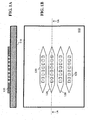
- Figs. 1A and 1B show several example conductors 120 that have been fabricated on an example substrate 110.
- the conductors are attached to the substrate with an adhesive.
- substrate 110 may be made from one or more of a material based on: silicon; glass; a polyimide; an acrylic; a cellophane; a mixture of some of these or other materials; a layered structure of these or other materials; or other materials.
- the conductivity of substrate 110 is relatively unimportant, but substrate 110 should be a material or set of materials that detach cleanly from conductors 120 at the appropriate time.
- Substrate 110 has an active surface that is substantially planar and to which conductors 120 are attached in such a manner that they can be later detached.
- Conductors 120 may be formed out of any conductive material.
- metals suitable for conductors 120 include, among others: gold; aluminum; copper; nickel; alloys of two or more of these or other metals; or layered or plated combinations of these or other metals or their alloys.
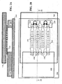
- Figs. 2A and 2B show the same example substrate and conductors, after the substrate is aligned with an example package.
- Package 240 holds electronic device 210 and opto-electronic device 220.
- Package 240 may be any material, device or mounting that secures electronic device 210 and opto-electronic device 220 device into a stable position relative to each other.
- At least one of the electronic devices to be interconnected is an opto-electronic device, which may include but is not limited to: a semiconductor laser; a photodiode; an electro-optic device; a light emitting diode; an electro-absorption modulator; a semiconductor optical amplifier; or a combination thereof.
- Each of electronic device 210 and opto-electronic device 220 has a surface that includes pads 230, each pad providing an electrical connection to a node of a circuit within the device.
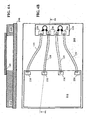
- Figs. 3A and 3B show the same example package with the electronic devices interconnected by the conductors after substrate 110 is removed.
- Conductors 120 are straight and flat, as shown in Figs. 1A , 2A and 3A ; that is, each conductor has a first planar surface and a second planar surface that are substantially parallel to each other. As shown in Figs. 1A and 2A , the first surface of each conductor is detachably attached to the active surface of substrate 110. As shown in Fig. 2A , the second surface of each conductor is substantially parallel and adjacent to two of pads 230. Then as shown in Fig. 3A , the second surface of each conductor is electronically connected and mechanically bonded to the two pads 230.
- conductors 120 are planar minimizes their length and thus advantageously reduces their parasitic electrical properties.
- conductors 120 are tapered and meshed in the plane of the active surface of substrate 110, or in the plane of the surface of pads 230.
- their ends can be narrowed to a size and shape suitable for bonding to pads of electronic or opto-electronic devices, yet the conductor can be wide for most of its length so as to reduce its parasitic inductance.
- a meshed conductor that is, one with a pattern of through holes along the length of the conductor, the parasitic capacitance of the conductor is reduced.
- the geometry of the conductors will be customized based on the details of the particular package and devices that are to be interconnected.
- the two dimensional shape of the conductors may have, among other shapes, a meshed shape, a tapered shape, a curved shape, a straight shape or a shape that is a combination of two or more of those shapes.
- the exact control of the size, shape and relative positions of the conductors afforded by the invention allows the inductance, capacitance and resistance of a conductor, or even the mutual inductance or capacitance between adjacent conductors, to be selected, tuned or adjusted as desired. This is advantageous in the design of systems that include opto-electronic devices, particularly in cases where the electrical properties of an opto-electronic device are complex or vary over time, such as is the case for an opto-electronic laser.
- the invention may produce more accurate control over the geometry of the conductors compared to interconnection techniques such as automated wire bonding or ribbon bonding that individually place conductors.
- Conductors with precisely controlled geometry and position can be used with pads on electronic devices that are smaller and that are closer together in pitch than conductors that individually differ in either or both of length and shape.
- This exact control of the conductors afforded by the invention also allows interconnection patterns to be used that are irregular because, for example, they may need to accommodate features of the optics part of the system.
- optical considerations are not always uniform or regular.
- some lens arrays may have additional spacing between some of the lenses for a device or material that provides additional mechanical strength or rigidity to the array.
- Figs. 4A and 4B show another example in which another example package has two devices that are interconnected by curved conductors.
- Curved conductors may or may not be additionally meshed, though non-meshed conductors are shown to clarify the drawing. Curved conductors, or conductors with even more irregular shape, may be useful in matching the pitch of pads 230 within electronic device 210 to the pitch of pads 230 within opto-electronic device 220.
- curved connectors advantageously allow the pitch at which adjacent opto-electronic devices 220 emit or receive light to be based on optical and mechanical considerations, and not on the size requirements of the circuitry or other features within electronic device 210.
- Substrate 110 is not shown here but it would be used as an interim device, as previously described.
- conductors 120 are held to substrate 110 using an adhesive material including, among others, an adhesive that holds a thin metallic film to a cellophane sheet or roll.
- the substrate may be ultraviolet (UV) tape that includes an adhesive that is sensitive to UV light and that loses its adhesive properties after sufficient exposure.
- UV ultraviolet
- the invention may be practiced using a completely rigid substrate, a flexible substrate, a compressible substrate, or a substrate with limited ability to flex or compress.
- Various degrees of rigidity in substrate 110 may be desirable to better work with the particular electronic or opto-electronic devices at hand and the particular packaging that holds these devices in place.
- some variation in the height of the pads of the devices mounted in the package can be accommodated by a substrate with an ability to flex or compress.
- the choice of a rigid substrate, a flexible substrate or a compressible substrate can support interconnecting a variety of device types using a variety of packaging techniques.
- the conductors are formed by photolithographic patterning to determine the two-dimensional shape of the conductors in the plane of the active surface of substrate 110. This allows complete control over the two-dimensional shape of the conductors. Then, electroplating may be use to obtain conductors of the desired thickness in the direction perpendicular to the active surface of substrate 110.
- a metallic film may be deposited on the major surface of substrate 110.
- a layer of photoresist may be deposited on the metallic film, and then photolithographically exposed with light that is patterned from a mask or reticle. The features in the mask or reticle are designed based on the particular interconnections to be made among the electronic or opto-electronic devices.
- the photoresist is then developed to remove the unwanted regions, as defined by the mask, and then the metallic film is etched away where it is not protected by the photoresist.
- the patterned metallic film is then subjected to an electroplating process, which results in conductors of the desired thickness being formed according to the two dimensional pattern of the mask or reticle.
- electroplating may allow the thickness of the conductor to be in the range of 10 to 50 micrometers ( ⁇ m).
- the conductors are formed by stamping a sheet of conductive material to determine the two-dimensional shape of the conductors. Using stamping to form the conductors may allow the thickness of the conductor to be in the range of 25 to 100 micrometers.
- All conductors are formed at the same time in embodiments of the invention that use photolithography to pattern the conductors, in embodiments that stamp the conductors out of a metal sheet, and in some other embodiments.
- Forming the conductors in a single operation has advantages over techniques such as ribbon or wire bonding in which each conductor must be individually formed and added.
- One such advantage is that manufacturing throughput is increased because substantially fewer operations are needed.
- Another advantage is that forming the conductors at the same time supports automated manufacturing better than interconnection techniques that form and add conductors one at a time. Automated manufacturing can, of course, reduce manufacturing cost and support volume production, both of which are particularly beneficial for systems that include optical communications links.
- a single alignment operation has advantages over techniques such as ribbon or wire bonding in which both ends of each ribbon or wire must be individually aligned.
- One such advantage is that manufacturing throughput is increased because substantially fewer alignment operations are needed.
- a single alignment operation can reduce manufacturing defects and field defects which may both be due to misalignment. Because a single alignment operation can be precisely controlled easier than multiple operations, the occurance of misaligned conductors can be reduced. Misaligned conductors can lead to open connections or to shorts between conductors or pads. Misaligned conductors can also lead to connections that are initially correct but will, over time, short or open. Thus both manufacturing defects and field defects may be reduced by employing the single alignment procedure described.
- Automated manufacturing can reduce manufacturing cost and can support volume production, both of which are particularly beneficial in systems that include optical communications links.
- the substrate 110 contains a through hole at a point where a particular conductor 120 contacts a particular pad 230.
- the bonding of the particular conductor to the particular pad may include inserting a bonding tip into the hole or directing a laser beam into the hole.
- substrate 110 is transparent at the wavelength of a laser and the bonding of conductors 120 to pads 230 includes passing a laser beam through the substrate.
- substrate 110 is simply pulled off the conductors after they are bonded to the devices.
- a relatively weak adhesive may be used, that is, an adhesive strong enough to keep conductors 120 attached to substrate 110 during handling but weak enough to allow the substrate to be easily detached after conductors 120 are bonded to pads 230.
- substrate 110 is detached from the conductors by altering the adhesion between the conductors and the substrate.
- the adhesion may be altered thermally, chemically, by exposure to light, by a combination thereof, or by some other process.
- the detachable substrate of the invention allows interconnecting electronic and opto-electronic devices that are tightly or densely packed within a package. Because substrate 110 is not present in the finished, packaged device, the electronic or opto-electronic devices that are interconnected can be closer together than is possible using other interconnection techniques, such as some tape array bonding (TAB) techniques. In some TAB bonding techniques, there must be significant separation between devices in order to accommodate a lead frame, tape, or other substrate that secure the conductors both during the packaging process and afterward in the finished device.
- TAB tape array bonding
- FIG. 3A and 3B An example of a package including plurality of electronic devices with conductors bonded to the pads of the devices is shown in Figs. 3A and 3B .
- Each conductor is self supporting between the devices, has a two dimensional shape and has a surface that is substantially parallel to an exposed surface of the pads.
- FIG. 1A and 1B An example of a substrate and a plurality of conductors configured to be used in interconnecting electronic devices, wherein the conductors are detachably attached to the substrate but otherwise physically independent of each other, is shown in Figs. 1A and 1B .
- the invention as described herein provides a method that enables interconnecting electronic devices including, among others, opto-electronic devices.
- the invention may be used to interconnect an electronic device with an opto-electronic device, to interconnect two electronic devices, one of which also interconnects with an opto-electronic device, or to interconnect electronic devices in a system that does not include opto-electronic devices.
Description
- The invention relates generally to a method of electrically interconnecting electronic devices and alternatively, to bonding planar electrical conductors to opto-electronic devices.
- Opto-electronic devices are semiconductor devices that emit light, that detect incoming light, or that alter and re-emit light. Modern research and technology have made the use of opto-electronic devices commonplace in the lives of many individuals, although for many people such use is unknowing.
- One major application of opto-electronic devices is in fiber optic communications. Over approximately the last two decades, fiber optic lines have taken over and transformed the long distance telephone industry. Optical fibers also play a dominant role in making the Internet available around the world. When optical fiber replaces copper wire for long distance calls and Internet traffic, costs are dramatically lowered and the rate at which information can be conveyed is increased.
- Optical fibers convey voice, Internet traffic and other information digitally at speeds or data rates that currently range upward from one gigabit per second, and that are expected to reach hundreds of gigabits per second or more. In order to achieve these data rates, an opto-electronic device emits a beam of light that is turned on and off at the data rate that is at upward of one billion times each second. On the other end of the fiber optic cable, another opto-electronic device receives that beam of light and detects the pattern with which it is turned on and off.
- Long distance fiber optical lines are commonplace. After a certain distance, light signals on optical fibers must be converted into electronic signals, electronically amplified and perhaps adjusted, and then re-emitted as light signals.
- Opto-electronic emitters must receive from electronic devices the information they send optically, and opto-electronic detectors must send to electronic devices the information they receive optically. At least for the electronic devices that connect directly to the opto-electronic devices, this information must be sent at the same data rate as the information is carried on the optical fiber.
- Unfortunately, at these data rates electronic interconnections can be problematic. The problems encountered include, among others, unintentional or parasitic effects. A wire that interconnects two electronic devices can create a small parasitic inductance and capacitance in the circuit, but at these data rates even small parasitic effects in circuits can have substantial effects on system performance. When such wires are placed close together, a parasitic coupling can be created between the signals on the two wires. Such parasitic effects distort the electronic signals on the wires, which can force the designers of opto-electronic systems to reduce the data rate at which the system operates, in order to reduce the effects of the distortions.
- The electrical conductors used at these data rates should be as short as possible in order to minimize parasitic effects such as capacitance and inductance.
- To increase bandwidth density, it is often preferable for the opto-electronic devices to be arranged in tightly spaced arrays. Bandwidth density measures the bandwidth of information that can be sent from, or received by, devices that fit within a unit of length along the side of a device, package or circuit board, or that fit within a unit of area of a device, package or circuit board. The former measure of bandwidth density can be expressed as gigabits per second per meter, and the latter measure as gigabits per second per square meter.
- Preferably, the spacing used in such arrays is determined by the optics part of the system, not the electronic devices that drive the opto-electronic devices. Arrays of opto-electronic devices may be used to transmit light signals that are conveyed by a ribbon-like bundle of optical fibers. Or, a single optical fiber that carries different signals at different wavelengths may be used with such an array, where each opto-electronic device in the array operates at a different wavelength.
- The electrical conductors used at these data rates should be as uniformly spaced as possible. This both prevents accidental connections between the conductors and minimizes parasitic coupling between the conductors.
- Other problems arise from the requirement that such opto-electronic devices be produced in volume. Millions of opto-electronic devices are in use today. Production rates in excess of one million units per month are occurring, or are projected for the immediate future. In order to meet these demands for volume production, the process of interconnecting opto-electronic devices with electronic devices must be inexpensive and reliable. This suggests that the interconnection process be highly automated.
-
US 6 242 280 B 1 discloses a method of interconnecting electronic devices in which an interconnect sheet is used that consists of conductors portions that are meant for forming the conductors and portions that are connecting the conductor portions. The interconnect sheet is aligned with the electronic devices, and the conductor portions are bonded to pads of the devices. After the bonding, the connecting portions of the interconnect sheet have to be separated from the conductor portions and removed from the device. This separation can be done by a laser process or by peeling the connecting portions of the device without damaging the conductor portions. - From
GB 1 223 704 - Tomimuro H. et al.: "New packaging technology GaAs MMIC modules" GALLIUM ARSENIDE IC SYMPOSIUM, SAN DIEGO; October 1989, pages 307-310, discloses a polyimide film on which a number of conductive elements are attached. The conductive elements are, however, not detachably attached to the film and the film is not removed from the conductor elements after the conductor elements are bonded to a device.
- The invention provides a solution to the problems described above by providing a novel method of interconnecting electronic devices including, among others, opto-electronic devices according to
claim 1. - The drawing illustrates technologies related to the invention, shows example embodiments of the invention, and gives examples of using the invention. The objects, features and advantages of the invention will become more apparent to those skilled in the art from the following detailed description, when read in conjunction with the accompanying drawing, wherein:
-
Figs. 1A and 1B respectively show, a view from the side along a cross sectional cut line and a view from the top of several example conductors that have been formed on a substrate and that have a tapered and meshed shape; -
Figs. 2A and 2B respectively show a cross section and a top view of the same example substrate and conductors after the substrate is aligned with an example package that holds two electronic devices; -
Figs. 3A and 3B respectively show a cross section and a top view of the same example package with the electronic devices interconnected by the conductors after the substrate is removed; and -
Figs. 4A and 4B respectively show a cross section and a top view of another example package with two electronic devices interconnected by curved conductors. - The descriptions and discussions herein illustrate technologies related to the invention, show examples of the invention and give examples of using the invention. Known methods, procedures, systems, circuits or components may be discussed without giving details, so as to avoid obscuring the principles of the invention. On the other hand, numerous details of specific examples of the invention may be described, even though such details may not apply to other embodiments of the invention. Details are included and omitted so as to better explain the invention and so as to aid in understanding the invention.
- In the drawing,
Figs. 1A and 1B showseveral example conductors 120 that have been fabricated on anexample substrate 110. In some embodiments of the invention, the conductors are attached to the substrate with an adhesive. - In various embodiments of the invention,
substrate 110 may be made from one or more of a material based on: silicon; glass; a polyimide; an acrylic; a cellophane; a mixture of some of these or other materials; a layered structure of these or other materials; or other materials. The conductivity ofsubstrate 110 is relatively unimportant, butsubstrate 110 should be a material or set of materials that detach cleanly fromconductors 120 at the appropriate time. -
Substrate 110 has an active surface that is substantially planar and to whichconductors 120 are attached in such a manner that they can be later detached. -
Conductors 120 may be formed out of any conductive material. Examples of metals suitable forconductors 120 include, among others: gold; aluminum; copper; nickel; alloys of two or more of these or other metals; or layered or plated combinations of these or other metals or their alloys. -
Figs. 2A and 2B show the same example substrate and conductors, after the substrate is aligned with an example package. -
Package 240 holdselectronic device 210 and opto-electronic device 220.Package 240 may be any material, device or mounting that secureselectronic device 210 and opto-electronic device 220 device into a stable position relative to each other. - In various embodiments of the invention, at least one of the electronic devices to be interconnected is an opto-electronic device, which may include but is not limited to: a semiconductor laser; a photodiode; an electro-optic device; a light emitting diode; an electro-absorption modulator; a semiconductor optical amplifier; or a combination thereof.
- Each of
electronic device 210 and opto-electronic device 220 has a surface that includespads 230, each pad providing an electrical connection to a node of a circuit within the device. -
Figs. 3A and 3B show the same example package with the electronic devices interconnected by the conductors aftersubstrate 110 is removed. -
Conductors 120 are straight and flat, as shown inFigs. 1A ,2A and3A ; that is, each conductor has a first planar surface and a second planar surface that are substantially parallel to each other. As shown inFigs. 1A and2A , the first surface of each conductor is detachably attached to the active surface ofsubstrate 110. As shown inFig. 2A , the second surface of each conductor is substantially parallel and adjacent to two ofpads 230. Then as shown inFig. 3A , the second surface of each conductor is electronically connected and mechanically bonded to the twopads 230. - Compared to wire bonds, ribbon bonds or other techniques in which each conductor is shaped into an arch as it is placed, the fact that
conductors 120 are planar minimizes their length and thus advantageously reduces their parasitic electrical properties. - In the example shown in
Figs. 1A through 3B ,conductors 120 are tapered and meshed in the plane of the active surface ofsubstrate 110, or in the plane of the surface ofpads 230. By tapering the conductors, their ends can be narrowed to a size and shape suitable for bonding to pads of electronic or opto-electronic devices, yet the conductor can be wide for most of its length so as to reduce its parasitic inductance. By using a meshed conductor, that is, one with a pattern of through holes along the length of the conductor, the parasitic capacitance of the conductor is reduced. - In practice, the geometry of the conductors will be customized based on the details of the particular package and devices that are to be interconnected. In various embodiments of the invention, the two dimensional shape of the conductors may have, among other shapes, a meshed shape, a tapered shape, a curved shape, a straight shape or a shape that is a combination of two or more of those shapes.
- The exact control of the size, shape and relative positions of the conductors afforded by the invention allows the inductance, capacitance and resistance of a conductor, or even the mutual inductance or capacitance between adjacent conductors, to be selected, tuned or adjusted as desired. This is advantageous in the design of systems that include opto-electronic devices, particularly in cases where the electrical properties of an opto-electronic device are complex or vary over time, such as is the case for an opto-electronic laser.
- This exact control of the conductors also allows the pads used as electronic connection points on the interconnected devices to be relatively small and close together in pitch. This is advantageous over interconnection techniques including, among others, wire bonding or ribbon bonding that manually place individual conductors between devices.
- Further, the invention may produce more accurate control over the geometry of the conductors compared to interconnection techniques such as automated wire bonding or ribbon bonding that individually place conductors. Conductors with precisely controlled geometry and position can be used with pads on electronic devices that are smaller and that are closer together in pitch than conductors that individually differ in either or both of length and shape.
- This exact control of the conductors afforded by the invention also allows interconnection patterns to be used that are irregular because, for example, they may need to accommodate features of the optics part of the system. In some systems, it is beneficial to set the positioning of opto-electronic devices based on optical considerations, such as the size and spacing of an array of lenses that receive the light emitted from (or that transmit light to) the opto-electronic devices or other optical considerations. Such optical considerations are not always uniform or regular. For example, some lens arrays may have additional spacing between some of the lenses for a device or material that provides additional mechanical strength or rigidity to the array.
-
Figs. 4A and 4B show another example in which another example package has two devices that are interconnected by curved conductors. Curved conductors may or may not be additionally meshed, though non-meshed conductors are shown to clarify the drawing. Curved conductors, or conductors with even more irregular shape, may be useful in matching the pitch ofpads 230 withinelectronic device 210 to the pitch ofpads 230 within opto-electronic device 220. In some embodiments of the invention, curved connectors advantageously allow the pitch at which adjacent opto-electronic devices 220 emit or receive light to be based on optical and mechanical considerations, and not on the size requirements of the circuitry or other features withinelectronic device 210.Substrate 110 is not shown here but it would be used as an interim device, as previously described. - In some embodiments of the invention,
conductors 120 are held tosubstrate 110 using an adhesive material including, among others, an adhesive that holds a thin metallic film to a cellophane sheet or roll. Alternatively, the substrate may be ultraviolet (UV) tape that includes an adhesive that is sensitive to UV light and that loses its adhesive properties after sufficient exposure. - The invention may be practiced using a completely rigid substrate, a flexible substrate, a compressible substrate, or a substrate with limited ability to flex or compress. Various degrees of rigidity in
substrate 110 may be desirable to better work with the particular electronic or opto-electronic devices at hand and the particular packaging that holds these devices in place. For example, some variation in the height of the pads of the devices mounted in the package can be accommodated by a substrate with an ability to flex or compress. The choice of a rigid substrate, a flexible substrate or a compressible substrate can support interconnecting a variety of device types using a variety of packaging techniques. - In some embodiments of the invention, the conductors are formed by photolithographic patterning to determine the two-dimensional shape of the conductors in the plane of the active surface of
substrate 110. This allows complete control over the two-dimensional shape of the conductors. Then, electroplating may be use to obtain conductors of the desired thickness in the direction perpendicular to the active surface ofsubstrate 110. - For example, a metallic film may be deposited on the major surface of
substrate 110. A layer of photoresist may be deposited on the metallic film, and then photolithographically exposed with light that is patterned from a mask or reticle. The features in the mask or reticle are designed based on the particular interconnections to be made among the electronic or opto-electronic devices. The photoresist is then developed to remove the unwanted regions, as defined by the mask, and then the metallic film is etched away where it is not protected by the photoresist. - In some embodiments of the invention, the patterned metallic film is then subjected to an electroplating process, which results in conductors of the desired thickness being formed according to the two dimensional pattern of the mask or reticle. Using electroplating to form the conductors may allow the thickness of the conductor to be in the range of 10 to 50 micrometers (µm).
- In other embodiments of the invention, the conductors are formed by stamping a sheet of conductive material to determine the two-dimensional shape of the conductors. Using stamping to form the conductors may allow the thickness of the conductor to be in the range of 25 to 100 micrometers.
- All conductors are formed at the same time in embodiments of the invention that use photolithography to pattern the conductors, in embodiments that stamp the conductors out of a metal sheet, and in some other embodiments. Forming the conductors in a single operation has advantages over techniques such as ribbon or wire bonding in which each conductor must be individually formed and added. One such advantage is that manufacturing throughput is increased because substantially fewer operations are needed.
- Another advantage is that forming the conductors at the same time supports automated manufacturing better than interconnection techniques that form and add conductors one at a time. Automated manufacturing can, of course, reduce manufacturing cost and support volume production, both of which are particularly beneficial for systems that include optical communications links.
- As shown in
Figs. 2A and 2B , by aligningsubstrate 110 withpackage 240, an end of every conductor is simultaneously aligned with arespective pad 230 ofdevices - A single alignment operation can reduce manufacturing defects and field defects which may both be due to misalignment. Because a single alignment operation can be precisely controlled easier than multiple operations, the occurance of misaligned conductors can be reduced. Misaligned conductors can lead to open connections or to shorts between conductors or pads. Misaligned conductors can also lead to connections that are initially correct but will, over time, short or open. Thus both manufacturing defects and field defects may be reduced by employing the single alignment procedure described.
- Further, it is easier to automate interconnection techniques that use a single alignment operation compared to techniques that use repeated alignment operations performed on individual conductors. Automated manufacturing can reduce manufacturing cost and can support volume production, both of which are particularly beneficial in systems that include optical communications links.
- In some embodiments of the invention, the
substrate 110 contains a through hole at a point where aparticular conductor 120 contacts aparticular pad 230. The bonding of the particular conductor to the particular pad may include inserting a bonding tip into the hole or directing a laser beam into the hole. - In other embodiments of the invention,
substrate 110 is transparent at the wavelength of a laser and the bonding ofconductors 120 topads 230 includes passing a laser beam through the substrate. - In some embodiments of the invention,
substrate 110 is simply pulled off the conductors after they are bonded to the devices. In such embodiments, a relatively weak adhesive may be used, that is, an adhesive strong enough to keepconductors 120 attached tosubstrate 110 during handling but weak enough to allow the substrate to be easily detached afterconductors 120 are bonded topads 230. - In other embodiments of the invention,
substrate 110 is detached from the conductors by altering the adhesion between the conductors and the substrate. The adhesion may be altered thermally, chemically, by exposure to light, by a combination thereof, or by some other process. - The detachable substrate of the invention allows interconnecting electronic and opto-electronic devices that are tightly or densely packed within a package. Because
substrate 110 is not present in the finished, packaged device, the electronic or opto-electronic devices that are interconnected can be closer together than is possible using other interconnection techniques, such as some tape array bonding (TAB) techniques. In some TAB bonding techniques, there must be significant separation between devices in order to accommodate a lead frame, tape, or other substrate that secure the conductors both during the packaging process and afterward in the finished device. - An example of a package including plurality of electronic devices with conductors bonded to the pads of the devices is shown in
Figs. 3A and 3B . Each conductor is self supporting between the devices, has a two dimensional shape and has a surface that is substantially parallel to an exposed surface of the pads. - An example of a substrate and a plurality of conductors configured to be used in interconnecting electronic devices, wherein the conductors are detachably attached to the substrate but otherwise physically independent of each other, is shown in
Figs. 1A and 1B . - Accordingly, the invention as described herein provides a method that enables interconnecting electronic devices including, among others, opto-electronic devices. The invention may be used to interconnect an electronic device with an opto-electronic device, to interconnect two electronic devices, one of which also interconnects with an opto-electronic device, or to interconnect electronic devices in a system that does not include opto-electronic devices.
- The invention may be practiced without the specific details described herein. The scope of the invention for which a patent is sought is set forth by the following claims.
Claims (7)
- A method of electrically interconnecting electronic devices, the method comprising:forming a plurality of planar electrical conductors (120) on an interim substrate (110);aligning the interim substrate (110) with at least two electronic devices (210,220), each electronic device (210,220) including at least one electrical connection pad (230), wherein each planar electrical conductor (120) is aligned in a single alignment operation with a respective electrical connection pad (230) on each of the at least two electronic devices (210,220);bonding each planar electrical conductor (120) to the respective electrical connection pads (230), thereby electrically interconnecting the at least two electronic devices (210,220); anddetaching the interim substrate (110) from the planar electrical conductors (120), wherein each planar electrical conductor (120) has a surface substantially parallel with a surface of the electrical connection pads (230).
- The method of claim 1,
wherein at least one of the electronic devices is a device selected from the group consisting of:an opto-electronic device; a semiconductor laser; a photodiode; an electro-optic device; a light emitting diode; an electro-absorption modulator; a semiconductor optical amplifier; and a combination thereof. - The method of claim 1 or 2,
wherein the interim substrate (110) contains a through hole at a point where a predetermined one of the planar electrical conductors (120) contacts a predetermined one of the electrical connection pads (230) and the bonding includes inserting a bonding tip into the through hole. - The method of claim 1 or 2,
wherein the interim substrate (110) contains a through hole at a point where a predetermined one of the planar electrical conductors (120) contacts a predetermined one of the electrical connection pads (230) and the bonding includes directing a laser beam into the through hole. - The method of claim 1 or 2,
wherein the interim substrate (110) is substantially transparent at the wavelength of a laser beam and the bonding includes directing the laser beam through the interim substrate (110) to a set of bonding points on the planar electrical conductors (120). - The method of one of claims 1 to 5,
wherein the detaching of the interim substrate (110) includes altering an adhesiveness between the planar electrical conductors (120) and the interim substrate (110). - The method of claim 6,
wherein the altering of the adhesiveness occurs via a process selected from the group consisting of: a thermal process: a chemical process; a light exposure process; and a combination thereof.
Applications Claiming Priority (2)
| Application Number | Priority Date | Filing Date | Title |
|---|---|---|---|
| US150303 | 2002-05-17 | ||
| US10/150,303 US6882044B2 (en) | 2002-05-17 | 2002-05-17 | High speed electronic interconnection using a detachable substrate |
Publications (3)
| Publication Number | Publication Date |
|---|---|
| EP1363327A2 EP1363327A2 (en) | 2003-11-19 |
| EP1363327A3 EP1363327A3 (en) | 2006-02-01 |
| EP1363327B1 true EP1363327B1 (en) | 2010-09-08 |
Family
ID=29269793
Family Applications (1)
| Application Number | Title | Priority Date | Filing Date |
|---|---|---|---|
| EP03002326A Expired - Fee Related EP1363327B1 (en) | 2002-05-17 | 2003-02-03 | Method providing electrical interconnection using a detachable substrate |
Country Status (4)
| Country | Link |
|---|---|
| US (1) | US6882044B2 (en) |
| EP (1) | EP1363327B1 (en) |
| JP (1) | JP2004006871A (en) |
| DE (1) | DE60334046D1 (en) |
Cited By (1)
| Publication number | Priority date | Publication date | Assignee | Title |
|---|---|---|---|---|
| CN101986770A (en) * | 2010-08-06 | 2011-03-16 | 深圳崇达多层线路板有限公司 | Multi-order high-density circuit board registration hole and manufacturing method thereof |
Families Citing this family (4)
| Publication number | Priority date | Publication date | Assignee | Title |
|---|---|---|---|---|
| US7304362B2 (en) * | 2002-05-20 | 2007-12-04 | Stmicroelectronics, Inc. | Molded integrated circuit package with exposed active area |
| JP4866625B2 (en) * | 2006-02-15 | 2012-02-01 | ルネサスエレクトロニクス株式会社 | Semiconductor device |
| WO2008059571A1 (en) * | 2006-11-15 | 2008-05-22 | Panasonic Corporation | Circuit board connection structure and circuit board |
| DE102014217985A1 (en) * | 2014-09-09 | 2016-03-10 | Robert Bosch Gmbh | Method for producing a bond pad, bond pad and bonding method |
Family Cites Families (13)
| Publication number | Priority date | Publication date | Assignee | Title |
|---|---|---|---|---|
| FR1483570A (en) * | 1965-06-23 | 1967-09-06 | ||
| GB1223705A (en) * | 1967-04-19 | 1971-03-03 | Hitachi Ltd | Semiconductor devices |
| JPS575356A (en) * | 1980-06-13 | 1982-01-12 | Toshiba Corp | Hybrid integrated circuit device |
| US5184207A (en) | 1988-12-07 | 1993-02-02 | Tribotech | Semiconductor die packages having lead support frame |
| JP2626203B2 (en) * | 1990-08-03 | 1997-07-02 | 富士ゼロックス株式会社 | Manufacturing method of electrophotographic photoreceptor |
| US5060052A (en) * | 1990-09-04 | 1991-10-22 | Motorola, Inc. | TAB bonded semiconductor device having off-chip power and ground distribution |
| US5309322A (en) | 1992-10-13 | 1994-05-03 | Motorola, Inc. | Leadframe strip for semiconductor packages and method |
| DE19603444C2 (en) * | 1996-01-31 | 2003-04-24 | Siemens Ag | LED device with at least two LEDs |
| KR19980020726A (en) | 1996-09-11 | 1998-06-25 | 김광호 | Chip scale ball grid array package and its manufacturing method |
| US6177722B1 (en) * | 1998-04-21 | 2001-01-23 | Atmel Corporation | Leadless array package |
| US6146813A (en) * | 1999-01-13 | 2000-11-14 | Applied Kinetics Inc. | Method and shunting and deshunting an electrical component and a shuntable/shunted electrical component |
| US6242280B1 (en) * | 1999-06-30 | 2001-06-05 | Agilent Technologies, Inc. | Method of interconnecting an electronic device |
| JP4441974B2 (en) * | 2000-03-24 | 2010-03-31 | ソニー株式会社 | Manufacturing method of semiconductor device |
-
2002
- 2002-05-17 US US10/150,303 patent/US6882044B2/en not_active Expired - Fee Related
-
2003
- 2003-02-03 EP EP03002326A patent/EP1363327B1/en not_active Expired - Fee Related
- 2003-02-03 DE DE60334046T patent/DE60334046D1/en not_active Expired - Lifetime
- 2003-05-16 JP JP2003138355A patent/JP2004006871A/en not_active Withdrawn
Cited By (2)
| Publication number | Priority date | Publication date | Assignee | Title |
|---|---|---|---|---|
| CN101986770A (en) * | 2010-08-06 | 2011-03-16 | 深圳崇达多层线路板有限公司 | Multi-order high-density circuit board registration hole and manufacturing method thereof |
| CN101986770B (en) * | 2010-08-06 | 2013-04-03 | 深圳崇达多层线路板有限公司 | Multi-order high-density circuit board registration hole and manufacturing method thereof |
Also Published As
| Publication number | Publication date |
|---|---|
| EP1363327A2 (en) | 2003-11-19 |
| US6882044B2 (en) | 2005-04-19 |
| DE60334046D1 (en) | 2010-10-21 |
| JP2004006871A (en) | 2004-01-08 |
| US20030213963A1 (en) | 2003-11-20 |
| EP1363327A3 (en) | 2006-02-01 |
Similar Documents
| Publication | Publication Date | Title |
|---|---|---|
| US6932522B2 (en) | Method and apparatus for hermetically sealing photonic devices | |
| US5054870A (en) | Electro-optical multiple connection arrangement | |
| US7476037B2 (en) | Apparatus for coupling a fiber optic cable to an optoelectronic device, a system including the apparatus, and a method of forming the same | |
| JP4425936B2 (en) | Optical module | |
| US6600853B2 (en) | Electro-optic interconnect circuit board | |
| CN112969946A (en) | Assembly of network switch ASIC and optical transceiver | |
| JP2004518156A (en) | Transparent substrate and hinged optical assembly | |
| JP2003279771A (en) | Light guide device, photoelectric fusion substrate, high speed serial bus, and their manufacturing method | |
| US7876984B2 (en) | Planar optical waveguide array module and method of fabricating the same | |
| KR100426039B1 (en) | Chip mounting method and device | |
| JPH04152682A (en) | Manufacture of sub-substrate for array-like optical element | |
| EP1363327B1 (en) | Method providing electrical interconnection using a detachable substrate | |
| US6860650B2 (en) | Assembly for aligning an optical array with optical fibers | |
| US5544269A (en) | Optical transmission module and method of forming the same | |
| JP2006047682A (en) | Substrate and substrate for interconnecting optical element | |
| JP2007057976A (en) | Optical module | |
| US20030068142A1 (en) | Optical subassembly for fiber arrays with a 90 degree conductor turn | |
| JPH03184384A (en) | Optical module submount and manufacture thereof | |
| US6350625B1 (en) | Optoelectronic packaging submount arrangement providing 90 degree electrical conductor turns and method of forming thereof | |
| JP4798863B2 (en) | Opto-electric wiring board | |
| EP3226046A1 (en) | Connection structure of optical fiber array and optical module | |
| US6787812B2 (en) | Active optical device | |
| WO2007023713A1 (en) | Optical module | |
| JPH11145487A (en) | Method and apparatus for manufacturing optical module | |
| JPH0933765A (en) | Optical module |
Legal Events
| Date | Code | Title | Description |
|---|---|---|---|
| PUAI | Public reference made under article 153(3) epc to a published international application that has entered the european phase |
Free format text: ORIGINAL CODE: 0009012 |
|
| AK | Designated contracting states |
Kind code of ref document: A2 Designated state(s): AT BE BG CH CY CZ DE DK EE ES FI FR GB GR HU IE IT LI LU MC NL PT SE SI SK TR |
|
| AX | Request for extension of the european patent |
Extension state: AL LT LV MK RO |
|
| PUAL | Search report despatched |
Free format text: ORIGINAL CODE: 0009013 |
|
| AK | Designated contracting states |
Kind code of ref document: A3 Designated state(s): AT BE BG CH CY CZ DE DK EE ES FI FR GB GR HU IE IT LI LU MC NL PT SE SI SK TR |
|
| AX | Request for extension of the european patent |
Extension state: AL LT LV MK RO |
|
| 17P | Request for examination filed |
Effective date: 20060704 |
|
| 17Q | First examination report despatched |
Effective date: 20060816 |
|
| AKX | Designation fees paid |
Designated state(s): DE FR GB |
|
| RAP1 | Party data changed (applicant data changed or rights of an application transferred) |
Owner name: AVAGO TECHNOLOGIES GENERAL IP (SINGAPORE) PTE. LTD |
|
| GRAP | Despatch of communication of intention to grant a patent |
Free format text: ORIGINAL CODE: EPIDOSNIGR1 |
|
| RIC1 | Information provided on ipc code assigned before grant |
Ipc: H01L 21/68 20060101AFI20100304BHEP |
|
| RTI1 | Title (correction) |
Free format text: METHOD PROVIDING ELECTRICAL INTERCONNECTION USING A DETACHABLE SUBSTRATE |
|
| GRAS | Grant fee paid |
Free format text: ORIGINAL CODE: EPIDOSNIGR3 |
|
| GRAA | (expected) grant |
Free format text: ORIGINAL CODE: 0009210 |
|
| AK | Designated contracting states |
Kind code of ref document: B1 Designated state(s): DE FR GB |
|
| REG | Reference to a national code |
Ref country code: GB Ref legal event code: FG4D |
|
| REF | Corresponds to: |
Ref document number: 60334046 Country of ref document: DE Date of ref document: 20101021 Kind code of ref document: P |
|
| PLBE | No opposition filed within time limit |
Free format text: ORIGINAL CODE: 0009261 |
|
| STAA | Information on the status of an ep patent application or granted ep patent |
Free format text: STATUS: NO OPPOSITION FILED WITHIN TIME LIMIT |
|
| 26N | No opposition filed |
Effective date: 20110609 |
|
| REG | Reference to a national code |
Ref country code: DE Ref legal event code: R097 Ref document number: 60334046 Country of ref document: DE Effective date: 20110609 |
|
| GBPC | Gb: european patent ceased through non-payment of renewal fee |
Effective date: 20110203 |
|
| REG | Reference to a national code |
Ref country code: FR Ref legal event code: ST Effective date: 20111102 |
|
| REG | Reference to a national code |
Ref country code: DE Ref legal event code: R119 Ref document number: 60334046 Country of ref document: DE Effective date: 20110901 |
|
| PG25 | Lapsed in a contracting state [announced via postgrant information from national office to epo] |
Ref country code: FR Free format text: LAPSE BECAUSE OF NON-PAYMENT OF DUE FEES Effective date: 20110228 |
|
| PG25 | Lapsed in a contracting state [announced via postgrant information from national office to epo] |
Ref country code: GB Free format text: LAPSE BECAUSE OF NON-PAYMENT OF DUE FEES Effective date: 20110203 |
|
| PG25 | Lapsed in a contracting state [announced via postgrant information from national office to epo] |
Ref country code: DE Free format text: LAPSE BECAUSE OF FAILURE TO SUBMIT A TRANSLATION OF THE DESCRIPTION OR TO PAY THE FEE WITHIN THE PRESCRIBED TIME-LIMIT Effective date: 20110901 |