EP1360766B1 - High -speed output driver - Google Patents
High -speed output driver Download PDFInfo
- Publication number
- EP1360766B1 EP1360766B1 EP01913703A EP01913703A EP1360766B1 EP 1360766 B1 EP1360766 B1 EP 1360766B1 EP 01913703 A EP01913703 A EP 01913703A EP 01913703 A EP01913703 A EP 01913703A EP 1360766 B1 EP1360766 B1 EP 1360766B1
- Authority
- EP
- European Patent Office
- Prior art keywords
- output
- driver
- transistor
- circuit
- series
- Prior art date
- Legal status (The legal status is an assumption and is not a legal conclusion. Google has not performed a legal analysis and makes no representation as to the accuracy of the status listed.)
- Expired - Lifetime
Links
Images

Classifications
-
- H—ELECTRICITY
- H03—ELECTRONIC CIRCUITRY
- H03K—PULSE TECHNIQUE
- H03K19/00—Logic circuits, i.e. having at least two inputs acting on one output; Inverting circuits
- H03K19/003—Modifications for increasing the reliability for protection
- H03K19/00369—Modifications for compensating variations of temperature, supply voltage or other physical parameters
- H03K19/00384—Modifications for compensating variations of temperature, supply voltage or other physical parameters in field effect transistor circuits
-
- H—ELECTRICITY
- H03—ELECTRONIC CIRCUITRY
- H03G—CONTROL OF AMPLIFICATION
- H03G3/00—Gain control in amplifiers or frequency changers without distortion of the input signal
- H03G3/20—Automatic control
- H03G3/30—Automatic control in amplifiers having semiconductor devices
Definitions
- the invention relates to a Hochgeschindtechniksausgangstreiber according to the preamble of claim 1.
- Such high-speed drivers are used in particular the connection of two digital circuits via waveguides, in particular 50 ohm lines or 75 ohm lines. They are formed in CMOS circuits with preferably low supply voltages ( ⁇ 2.5 volts).
- a basic element of such high-speed output drivers is a differential driver or a "single-ended" driver according to FIGS. 1 and 2.
- a differential driver comprises two standard CMOS inverters with n-channel MOS transistors T1, T3 and complementary p-channel MOS transistors T2, T4 on.
- the two inverters are operated via input nodes I, In with a differential input voltage Uin.
- the output voltage Uout is taken off.
- Such a differential driver provides a push-pull output.
- a single-ended driver according to FIG. 2 has a standard CMOS inverter with an n-channel MOS transistor T1 and a p-channel MOS transistor T2, which are connected in series.
- the CMOS inverter operates on a load R3 of typically 50 ohms, at which a reference voltage Vref is applied.
- the reference voltage Vref corresponds, for example, to half the supply voltage (single-ended output).
- circuits shown in Figures 1 and 2 represent basic circuits, which for the concrete Use case obtained by dimensioning the required properties.
- the drain-source resistances of the transistors are adjusted according to the desired application.
- CMOS inverters or drivers A disadvantage of the known CMOS inverters or drivers, however, is that the transistor properties are subject to high fluctuations. These fluctuations result in particular from temperature fluctuations and parameter fluctuations in the manufacturing process. The properties of the transistors of the CMOS inverter are thus subject to high fluctuations over the temperature and the manufacturing process. These variations can be up to 100 percent in the applications described.
- CMOS inverter with an n-channel transistor and a complementary p-channel transistor connected in series can be digitally connected to other CMOS inverters.
- US-A-5 581 197 describes a CMOS output driver with a CMOS inverter to which transistors are connected in series by analogue control signals to keep the output resistance of the driver constant.
- the present invention has for its object to provide a further high-speed output driver with a serving as an amplifier for digital signals CMOS inverter available, which is characterized by a substantially constant output current and a substantially constant output resistance.
- Additional transistors are provided which connect the circuit means for controlling the output current and the output resistance of the driver to the CMOS inverter in series via analogue control signals, at least one additional transistor in series with the n-channel transistor and at least one additional transistor in Series is connected to the p-channel transistor of the inverter.
- a separate, independent control circuit in the form of a regulated mirror circuit is provided for each additional transistor, which regulates the operating point of the respective additional transistor.
- the connected transistors are preferably each operated in the triode region, in which a transistor is a linear resistor.
- the additionally provided by the transistor resistance is in this area substantially linearly dependent on the voltage applied to the gate terminal.
- the elements of the mirror circuit preferably correspond in their size to the elements of the driver circuit or are scaled to the latter by a certain value.
- the power consumption can be reduced by a factor of 1 / n.
- the mirror circuit preferably includes an operational amplifier which controls the control voltage for the mirror circuit to a value such that the desired output level at the output of the mirror circuit and thus also sets the output of the driver.
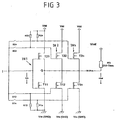
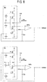
- FIGS. 3 to 8 relate to circuit variants in which a single-ended circuit according to FIG. 2 is used.
- the following embodiments are also applicable in a corresponding manner also for differential circuits according to Figure 1, since they are basically constructed symmetrically.
- a first inverter IN1 which consists of a p-channel MOS transistor T21 and an n-channel MOS transistor T11, which are complementary and connected in series.
- a digital input signal Uin At an input node I is applied to a digital input signal Uin and at an output node Q, a likewise digital output signal is tapped.
- the transistor T11 is connected with its source terminal to the reference potential Vss (GROUND) and the transistor T21 with its source terminal to the operating voltage Vdd.
- CMOS inverters are known per se.
- inverters IN2 to INn which have transistors T12, T22 or T1n, T2n and are arranged parallel to the inverter IN1 are now connected behind the output Q of the first inverter IN1.
- additional inverters can be connected, wherein only two additional inverters IN2, INn are shown in FIG.
- the gate terminals of the transistors of the further inverters IN2, INn are, like the gate terminals of the transistors of the inverter IN1, at the reference point I and thus at the input voltage Uin.
- the connection is made, however via switches S12, S1n, S22, S2n, via whose control the connection of the further inverters IN2 to INn can be controlled.
- the gate terminals of the transistors of the further inverters IN2, INn are connected to the operating voltage Vdd or GROUND via resistors R22, R2n and R12, R1n, respectively.
- the resistors are used with the switch open S12, S1n, S22, S2n to pull the gate terminal to GROUND or Vdd, so that the respective inverter IN2 to INn are disabled.
- the transistors T12, T22, T1n, T2n are then high-impedance.
- the fine adjustment of the total impedance is made by selecting the size of the transistors of the additional inverters IN2, INn. These are preferably weighted and are approximately 1, 2, 3, 4, ... 2 n times the size of the transistors T11, T12 of the inverter IN1.
- At the output Q of the driver circuit is a 50 ohm line with a terminating resistor R3 of preferably also 50 ohms.
- the (50 ohm) resistor R3 is connected to a reference voltage Vref.
- the output voltage Uout dropping at the output resistance R3 depends on the number of inverters IN1, IN2, ... INn arranged in parallel.
- a suitable addition or removal of the parallel arranged inverters IN2, INn via the switches S12, S1n, S22, S2n a constant output current and a constant output resistance of the driver circuit can be provided.
- the output current is increased and the output resistance is reduced, since the further inverter provide an additional current path applied to the output node Q.
- the output resistance increases due to changed transistor characteristics, this can be compensated by adding another inverter.
- a decreasing output resistance be compensated.
- the circuit shown is further characterized by the fact that it manages with extremely small supply voltages with Vdd of 1 ... 1.8 volts. This allows very fast circuits with a clock frequency of up to several gigahertz, as they are needed for modern technologies realize.
- the illustrated high speed output driver is preferably used to connect two circuits on a printed circuit board by means of a 50 ohm line. It provides an interface to other circuits.
- the control unit S1 is connected to a temperature sensor TS and a process sensor PS, the analog input signals to the control unit S1.
- the temperature sensor TS supplies an input signal to the control unit S1, which represents a measure of the temperature of the transistors T11, T21 of the inverter IN1.
- the temperature sensor is disposed in close proximity to the CMOS inverter on a common substrate.
- the process sensor PS provides an input signal representing a measure of process parameters of the transistors.
- the process sensor PS measures, for example, the output impedance or the output current of a comparable transistor and outputs a corresponding signal to the control unit S1. This in turn generates appropriate control signals for the switches S12, S1n, S22, S2n.
- the process sensor can also form a unit together with the temperature sensor.
- control unit S1 On the basis of these input signals, the control unit S1 generates control signals for the switches S11, S1n, S21, S2n, with which the switches are actuated and the respective inverters IN2 until INn is switched on or off.
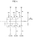
- the high-speed output driver of Figure 4 corresponds essentially to the driver of Figure 3, so that reference is made to the statements there. The difference is that the switches S12, S1N and S22, S2n control the sources of the transistors T12, T22, T1n, T2n instead of the gate terminals.
- the resistors R12, R1n, R22, R2n according to FIG. 3 are dispensed with. A possible weighting of the size of the transistors takes place directly via the choice of the transistors.
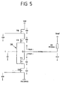
- FIG. 5 shows an alternative embodiment of the invention in which an analog control of an inverter IN takes place.
- the inverter IN itself is implemented as described with reference to FIG. 3 and has an n-channel transistor T1 and a p-channel transistor T2.
- a further p-channel transistor T6 is now connected in series between the source terminal of the transistor T2 and the operating voltage Vdd, whose gate terminal is supplied with a control voltage Ust6.
- a further n-channel transistor T5 is connected between the source terminal of the transistor T1 and the potential Vss (GROUND), whose gate terminal is supplied with a control voltage Ust5.
- either the transistors T2 and T6 or T1 and T5 are conductive, with the respective resistors Rd2, Rd6 and Rd1, Rd5 arising at the individual transistors becoming output resistors Rout2 of the upper arm and Rout1 of the lower arm add.
- the additional transistor T5 is now chosen to be large and completely controlled, so that the total resistance Rout1 this branch is essentially determined by Rd5.
- the control voltage Ust5 then the resistance or current flow of the inverter can be controlled.
- the transistor T5 is operated in the triode region, that is it represents a linear resistor Control of the output impedance of the driver possible.
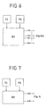
- a control unit S2 For controlling the voltages Ust5 and Ust6, a control unit S2 according to FIG. 7 is provided.
- the control unit S2 is in turn connected to the output signals of a temperature sensor TS and a process sensor PS. In contrast to the control unit of FIG. 6, however, analog output signals Ust5 and Ust6 are generated.
- FIG 8 shows a development of the invention is shown, in which not only a control of the output parameters of the inverter IN takes place, but a scheme.
- two mirror circuits Sa and Sd are provided for generating the control voltages Ust5 and Ust6 for the circuit according to FIG.
- the mirror circuits Sa and Sd are constructed such that their elements correspond to the elements of the actual driver circuit according to FIG. Corresponding elements of the mirror circuit are additionally denoted by the letters "a" and "b".
- the mirror elements of the mirror circuit Sa, Sb can either have the same size as the corresponding elements of the driver circuit or a scaling of the mirror elements can be provided in order to reduce the current consumption of the mirror circuit.
- a scaling factor n by which the current consumption of the mirror circuit is reduced, but without changing their properties, the transistors T2a, T6a, T1a and T5a of the mirror circuit Sa are smaller by a factor of 1 / n and the resistance R3a by a factor of n as the corresponding parts of the output driver of Figure 5. The same applies to the elements of the mirror circuit Sb.
- the node Ia or Ib of the mirror circuits Sa, Sb is set to the respective logic level (HIGH, LOW).
- the inverted, amplified signal is present at the output Qa or Qb.
- the output Qa or Qb is connected to the non-inverted input of an operational amplifier OPa or OPb.
- the inverted input of the operational amplifier OPa, OPb is connected via a capacitor Ca or Cb to the gate terminal of the transistor T5a and T6b.
- the output of the operational amplifier is connected directly to the gate of transistor T5a and T6b, respectively.
- the output of the operational amplifier OPa or OPb provides the control voltage Ust5 or Ust6 for the driver of FIG.
- the respective operational amplifier OPa, OPb regulates the control voltage Ust5a, Ust6b to a value such that the desired output level is set to Qa or Qb.
- the specification (setpoint) is made in each case by the voltage Ureflow or Urefhigh at the inverted input of the operational amplifier.
- control voltages Ust6a in the circuit part Sa and Ust5b in the circuit part Sb are not relevant since the upstream transistor T2a in Sa and T1b in Sb is blocked.
- the transistors T6a and T5b can thus also be disabled or eliminated.
- circuit means are provided which control the output current and the output resistance of a high-speed output driver in response to input parameters to a substantially constant value, wherein a connection or switching off additional, integrated in the driver transistors.
Description
Die Erfindung betrifft einen Hochgeschindigkeitsausgangstreiber nach dem Oberbegriff des Anspruchs 1. Derartige Hochgeschwindigkeitstreiber dienen insbesondere der Verbindung zweier digitaler Schaltungen über Wellenleiter, insbesondere 50-Ohm-Leitungen oder 75-Ohm-Leitungen. Sie sind in CMOS-Schaltungen mit vorzugsweise kleinen Versorgungsspannungen (< 2,5 Volt) ausgebildet.The invention relates to a Hochgeschindigkeitsausgangstreiber according to the preamble of
Ein Grundelement derartiger Hochgeschwindigkeitsausgangstreiber ist ein differenzieller Treiber oder ein "single ended" Treiber gemäß den Figuren 1 und 2. Gemäß Figur 1 weist ein differenzieller Treiber zwei Standard-CMOS-Inverter mit n-Kanal MOS-Transistoren T1, T3 und komplementären p-kanal MOS-Transistoren T2, T4 auf. Die beiden Inverter werden mit über Eingangsknoten I, In mit einer differentiellen Eingangsspannung Uin betrieben. An den Knotenpunkten Q, Qn der Drain-Anschlüsse der beiden Inverter wird die Ausgangsspannung Uout abgenommen. Am Ausgang Q, Qn liegt eine differentielle Last R3 von üblicherweise 2x50 Ohm = 100 Ohm an. Ein solcher differenzieller Treiber stellt einen Gegentaktausgang zur Verfügung.A basic element of such high-speed output drivers is a differential driver or a "single-ended" driver according to FIGS. 1 and 2. According to FIG. 1, a differential driver comprises two standard CMOS inverters with n-channel MOS transistors T1, T3 and complementary p-channel MOS transistors T2, T4 on. The two inverters are operated via input nodes I, In with a differential input voltage Uin. At the nodes Q, Qn of the drain terminals of the two inverters, the output voltage Uout is taken off. At the output Q, Qn is a differential load R3 of usually 2x50 ohms = 100 ohms. Such a differential driver provides a push-pull output.
Ein "single ended" Treiber gemäß Figur 2 weist einen Standard-CMOS-Inverter mit einem n-Kanal-MOS-Transistor T1 und einem p-Kanal-MOS-Transistor T2 auf, die in Reihe geschaltet sind. Der CMOS-Inverter arbeitet auf eine Last R3 von üblicherweise 50 Ohm, an der eine Referenzspannung Vref liegt. Die Referenzspannung Vref entspricht beispielsweise der halben Versorgungsspannung (Eintaktausgang).A single-ended driver according to FIG. 2 has a standard CMOS inverter with an n-channel MOS transistor T1 and a p-channel MOS transistor T2, which are connected in series. The CMOS inverter operates on a load R3 of typically 50 ohms, at which a reference voltage Vref is applied. The reference voltage Vref corresponds, for example, to half the supply voltage (single-ended output).
Die in den Figuren 1 und 2 dargestellten Schaltungen stellen prinzipielle Schaltungen dar, welche für den konkreten Anwendungsfall durch Dimensionierung die geforderten Eigenschaften erhalten. Insbesondere werden die Drain-Source-Widerstände der Transistoren entsprechend der gewünschten Anwendung eingestellt.The circuits shown in Figures 1 and 2 represent basic circuits, which for the concrete Use case obtained by dimensioning the required properties. In particular, the drain-source resistances of the transistors are adjusted according to the desired application.
Ein Nachteil an den bekannten CMOS-Invertern bzw. Treiber besteht allerdings darin, daß die Transistoreigenschaften hohen Schwankungen unterworfen sind. Diese Schwankungen ergeben sich insbesondere aus Temperaturschwankungen und aus Parameterschwankungen beim Herstellungsprozeß. Die Eigenschaften der Transistoren der CMOS-Inverter unterliegen somit hohen Schwankungen über der Temperatur und dem Herstellungsprozeß. Diese Schwankungen können in den beschriebenen Anwendungen bei bis zu 100 Prozent liegen.A disadvantage of the known CMOS inverters or drivers, however, is that the transistor properties are subject to high fluctuations. These fluctuations result in particular from temperature fluctuations and parameter fluctuations in the manufacturing process. The properties of the transistors of the CMOS inverter are thus subject to high fluctuations over the temperature and the manufacturing process. These variations can be up to 100 percent in the applications described.
Andererseits besteht für die genannten Hochgeschwindigkeitsausgangstreiber das Erfordernis, daß diese
- 1. an einer externen Last, etwa einer 50-Ohm-Leitung mit Abschlußwiderstand, einen konstanten Ausgangspegel, d.h. einen relativ konstanten Ausgangsstrom aufweisen und
- 2. der Treiber einen relativ konstanten Ausgangswiderstand aufweist, um Reflektionen an der Quelle zu vermeiden. Der Treiber sollten dabei möglichst eine aktive Last in Form eines schaltenden Transistors aufweisen, da passive Lasten den Stromverbrauch erhöhen bzw. bei kleinen Spannung nicht einsetzbar sind.
- 1. at an external load, such as a 50 ohm line with terminating resistor, a constant output level, ie have a relatively constant output current and
- 2. The driver has a relatively constant output resistance to avoid reflections at the source. The driver should have as much as possible an active load in the form of a switching transistor, since passive loads increase the power consumption or can not be used at low voltage.
Die beiden vorgenannten Forderungen lassen sich mit herkömmlichen CMOS-Invertern aufgrund der erläuterten Schwankungen der Transistoreigenschaften über Temperatur und Herstellungsprozeß nicht verwirklichen. Es besteht daher ein Bedürfnis, die bekannten CMOS-Inverter bzw. Treiberschaltungen mit derartigen Invertern derart weiterzubilden, daß konstante Ausgangsbedingungen, d.h. ein im wesentlichen konstanter Ausgangsstrom und ein im wesentlichen konstanter Ausgangswiderstand des Treibers vorliegen.The two aforementioned requirements can not be realized with conventional CMOS inverters due to the explained variations in the transistor properties over temperature and manufacturing process. There is therefore a need to develop the known CMOS inverter or driver circuits with such inverters such that constant output conditions, ie a substantially constant output current and a substantially constant output resistance of the driver are present.
In der Veröffentlichung "Itanium™ Processor System Bus Design" A. Ilkbahar, S. Venkataraman, H. Muljono, ESSCIRC 2000, Stockholm 19.-21. September 2000, S. 128 - 131 ist eine Ausgangstreiberschaltung für den Itanium™-Processor der Firma Intel beschrieben, bei der einem Inverter zur Einstellung einer gewünschten Ausgangsimpedanz diskret parallele Inverter zugeschaltet werden. Jedoch erfolgt dies im Hinblick auf eine Anpassung des Treibers an variable kapazitive Ausgangslasten.In the publication "Itanium ™ Processor System Bus Design" A. Ilkbahar, S. Venkataraman, H. Muljono, ESSCIRC 2000, Stockholm 19.-21. September 2000, pp. 128-131, an output driver circuit for the Itanium ™ processor from Intel is described, in which an inverter is switched to set a desired output impedance discrete parallel inverters. However, this is done in terms of adapting the driver to variable output capacitive loads.
Aus der US-A-5 621 335 ist ein gattungsgemäßer Hochgeschwindigkeitstreiber bekannt. Einem CMOS Inverter mit einem n-Kanal Transistor und einem dazu in Reihe geschalteten, komplementären p-Kanal Transistor sind digital weitere CMOS Inverter zuschaltbar.From US-A-5 621 335 a generic high speed driver is known. A CMOS inverter with an n-channel transistor and a complementary p-channel transistor connected in series can be digitally connected to other CMOS inverters.
Die US-A-5 581 197 beschreibt einen CMOS Ausgangstreiber mit einem CMOS-Inverter, dem Transistoren durch analoge Steuersignale in Reihe zugeschaltet werden, um den Ausgangswiderstand des Treibers konstant zu halten.US-A-5 581 197 describes a CMOS output driver with a CMOS inverter to which transistors are connected in series by analogue control signals to keep the output resistance of the driver constant.
Der vorliegenden Erfindung liegt die Aufgabe zugrunde, einen weiteren Hochgeschwindigkeitsausgangstreiber mit einem als Verstärker für digitale Signale dienenden CMOS-Inverter zur Verfügung zu stellen, der sich durch einen im wesentlichen konstanten Ausgangsstrom und einen im wesentlichen konstanten Ausgangswiderstand auszeichnet.The present invention has for its object to provide a further high-speed output driver with a serving as an amplifier for digital signals CMOS inverter available, which is characterized by a substantially constant output current and a substantially constant output resistance.
Diese Aufgabe wird erfindungsgemäß durch einen Hochgeschwindigkeitsausgangstreiber mit den Merkmalen des Anspruchs 1 gelöst. Vorteilhafte und bevorzugte Ausgestaltungen der Erfindung sind in den Unteransprüchen angegeben.This object is achieved by a high-speed output driver with the features of
Es sind zusätzliche Transistoren vorgesehen, die die Schaltungsmittel zur Steuerung oder Regelung des Ausgangsstroms und des Ausgangswiderstands des Treibers dem CMOS-Inverter über analoge Steuersignale in Reihe zuschalten, wobei mindestens ein zusätzlicher Transistor in Reihe mit dem n-Kanal Transistor und mindestens ein zusätzlicher Transistor in Reihe mit dem p-Kanal Transistor des Inverters geschaltet ist. Erfindungsgemäß ist dabei für jeden zusätzlichen Transistor eine gesonderte, unabhängige Regelschaltung in Form einer geregelten Spiegelschaltung vorgesehen, die den Arbeitspunkt des jeweiligen zusätzlichen Transistors regelt.Additional transistors are provided which connect the circuit means for controlling the output current and the output resistance of the driver to the CMOS inverter in series via analogue control signals, at least one additional transistor in series with the n-channel transistor and at least one additional transistor in Series is connected to the p-channel transistor of the inverter. According to the invention, a separate, independent control circuit in the form of a regulated mirror circuit is provided for each additional transistor, which regulates the operating point of the respective additional transistor.
Zur Regelung (mit Rückkopplung) werden somit analog zusätzliche Transistoren zugeschaltet, die die Ausgangseigenschaften des Treibers verändern, insbesondere dessen Drain-Source-Widerstand. Das Zuschalten von einzelnen Transistoren zur Änderung der Ausgangseigenschaften des Treibers erfolgt über eine analoge Steuerung.To control (with feedback) thus analog additional transistors are switched, which change the output characteristics of the driver, in particular its drain-source resistance. The connection of individual transistors to change the output characteristics of the driver via an analog controller.
Die zugeschalteten Transistoren werden bevorzugt jeweils im Triodenbereich betrieben, in dem ein Transistor einen linearen Widerstand darstellt. Der durch den Transistor zusätzlich zur Verfügung gestellte Widerstand ist in diesem Bereich im wesentlichen linear von der am Gate-Anschluß anliegenden Spannung abhängig.The connected transistors are preferably each operated in the triode region, in which a transistor is a linear resistor. The additionally provided by the transistor resistance is in this area substantially linearly dependent on the voltage applied to the gate terminal.
Die Elemente der Spiegelschaltung entsprechen bevorzugt in ihrer Größe den Elementen der Treiberschaltung oder sind gegenüber letzteren um einen bestimmten Wert skaliert. Durch eine Skalierung um den Faktor n kann die Stromaufnahme um den Faktor 1/n reduziert werden.The elements of the mirror circuit preferably correspond in their size to the elements of the driver circuit or are scaled to the latter by a certain value. By scaling by the factor n, the power consumption can be reduced by a factor of 1 / n.
Die Spiegelschaltung enthält bevorzugt einen Operationsverstärker, der die Steuerspannung für die Spiegelschaltung auf einen Wert derart regelt, daß sich der gewünschte Ausgangspegel am Ausgang der Spiegelschaltung und damit auch am Ausgang des Treibers einstellt.The mirror circuit preferably includes an operational amplifier which controls the control voltage for the mirror circuit to a value such that the desired output level at the output of the mirror circuit and thus also sets the output of the driver.
Die Erfindung wird nachfolgend unter Bezugnahme auf die Figuren der Zeichnung anhand mehrerer Ausführungsbeispiele näher erläutert. Es zeigen:
- Figur 1 -
- einen differentiellen Ausgangstreiber gemäß dem Stand der Technik;
- Figur 2 -
- einen "single ended" Ausgangstreiber gemäß dem Stand der Technik;
- Figur 3 -
- ein erstes Ausführungsbeispiel eines digital geschalteten, erfindungsgemäßen Treibers mit Steuerung der Gate-Anschlüsse;
- Figur 4 -
- ein zweites Ausführungsbeispiel eines digital geschalteten, erfindungsgemäßen Treibers mit Steuerung der Source-Anschlüsse;
- Figur 5 -
- ein Ausführungsbeispiel eines erfindungsgemäßen Treibers mit analoger Steuerung;
- Figur 6 -
- eine digitale Steuereinheit für einen erfindungsgemäßen Ausgangstreiber;
- Figur 7 -
- eine analoge Steuereinheit für einen erfindungsgemäßen Ausgangstreiber und
- Figur 8 -
- zwei Spiegelschaltungen zur Regelung der Steuerspannungen des Treibers der Figur 5.
- FIG. 1 -
- a differential output driver according to the prior art;
- FIG. 2 -
- a "single ended" output driver according to the prior art;
- FIG. 3 -
- A first embodiment of a digitally connected, inventive driver with control of the gate terminals;
- FIG. 4 -
- a second embodiment of a digitally switched, inventive driver with control of the source terminals;
- FIG. 5 -
- an embodiment of a driver according to the invention with analog control;
- FIG. 6 -
- a digital control unit for an output driver according to the invention;
- FIG. 7 -
- an analog control unit for an output driver according to the invention and
- FIG. 8 -
- two mirror circuits for controlling the control voltages of the driver of Figure 5.
Die prinzipiellen Grundschaltungen eines erfindungsgemäßen Hochgeschwindigkeitsausgangstreibers waren eingangs anhand der Figuren 1 und 2 erläutert worden. Es wird darauf hingewiesen, daß die nachfolgenden Ausführungsbeispiele der Figuren 3 bis 8 Schaltungsvarianten betreffen, in denen eine Eintaktschaltung gemäß Figur 2 verwendet wird. Die nachfolgenden Ausführungsbeispiele sind jedoch in entsprechender Weise ebenfalls für differentielle Schaltungen gemäß Figur 1 anwendbar, da diese grundsätzlich symmetrisch aufgebaut sind.The basic basic circuits of a high-speed output driver according to the invention were explained in the introduction with reference to FIGS. 1 and 2. It should be noted that the following embodiments of the FIGS. 3 to 8 relate to circuit variants in which a single-ended circuit according to FIG. 2 is used. However, the following embodiments are also applicable in a corresponding manner also for differential circuits according to Figure 1, since they are basically constructed symmetrically.
Gemäß Figur 3 ist ein erster Inverter IN1 vorgesehen, der aus einem p-Kanal MOS-Transistor T21 und einem n-Kanal MOS-Transistor T11 besteht, die komplementär ausgebildet und in Reihe geschaltet sind. An einem Eingangsknoten I liegt ein digitales Eingangssignal Uin an und an einem Ausgangsknoten Q wird ein ebenfalls digitales Ausgangssignal abgegriffen. Der Transistor T11 ist mit seinem Source-Anschluß mit dem Bezugspotential Vss (GROUND) und der Transistor T21 mit seinem Source-Anschluß mit der Betriebsspannung Vdd verbunden.According to Figure 3, a first inverter IN1 is provided, which consists of a p-channel MOS transistor T21 and an n-channel MOS transistor T11, which are complementary and connected in series. At an input node I is applied to a digital input signal Uin and at an output node Q, a likewise digital output signal is tapped. The transistor T11 is connected with its source terminal to the reference potential Vss (GROUND) and the transistor T21 with its source terminal to the operating voltage Vdd.
Wenn an dem Eingangsknoten I die Eingangsspannung LOW anliegt, sperrt der Transistor T11 und wird der Ausgang Q auf die Betriebsspannung Vdd gezogen. Wenn dagegen die Eingangsspannung am Eingangsknoten I den Wert HIGH annimmt, sperrt der obere Transistor T21 und wird der Ausgang Q auf Ground gezogen. Derartige CMOS-Inverter sind an sich bekannt.When the input voltage LOW is applied to the input node I, the transistor T11 turns off and the output Q is pulled to the operating voltage Vdd. In contrast, if the input voltage at the input node I takes the value HIGH, the upper transistor T21 turns off and the output Q is pulled to ground. Such CMOS inverters are known per se.
Erfindungsgemäß sind nun hinter den Ausgang Q des ersten Inverters IN1 weitere Inverter IN2 bis INn geschaltet, die Transistoren T12, T22 bzw. T1n, T2n aufweisen und parallel zum Inverter IN1 angeordnet sind. Grundsätzlich können dabei eine beliebige Zahl von zusätzlichen Invertern zugeschaltet sein, wobei in Figur 3 lediglich zwei zusätzliche Inverter IN2, INn dargestellt sind.According to the invention, further inverters IN2 to INn which have transistors T12, T22 or T1n, T2n and are arranged parallel to the inverter IN1 are now connected behind the output Q of the first inverter IN1. In principle, an arbitrary number of additional inverters can be connected, wherein only two additional inverters IN2, INn are shown in FIG.
Die Gate-Anschlüsse der Transistoren der weiteren Inverter IN2, INn liegen ebenso wie die Gate-Anschlüsse der Transistoren des Inverters IN1 am Bezugspunkt I und damit an der Eingangsspannung Uin. Die Verbindung erfolgt allerdings über Schalter S12, S1n, S22, S2n, über deren Steuerung die Zuschaltung der weiteren Inverter IN2 bis INn steuerbar ist.The gate terminals of the transistors of the further inverters IN2, INn are, like the gate terminals of the transistors of the inverter IN1, at the reference point I and thus at the input voltage Uin. The connection is made, however via switches S12, S1n, S22, S2n, via whose control the connection of the further inverters IN2 to INn can be controlled.
Die Gate-Anschlüsse der Transistoren der weiteren Inverter IN2, INn sind über Widerstände R22, R2n bzw. R12, R1n mit der Betriebsspannung Vdd bzw. GROUND verbunden. Die Widerstände dienen dazu, bei geöffnetem Schalter S12, S1n, S22, S2n den Gate-Anschluß auf GROUND bzw. Vdd zu ziehen, damit die jeweiligen Inverter IN2 bis INn gesperrt sind. So sind die Transistoren T12, T22, T1n, T2n dann hochohmig.The gate terminals of the transistors of the further inverters IN2, INn are connected to the operating voltage Vdd or GROUND via resistors R22, R2n and R12, R1n, respectively. The resistors are used with the switch open S12, S1n, S22, S2n to pull the gate terminal to GROUND or Vdd, so that the respective inverter IN2 to INn are disabled. Thus, the transistors T12, T22, T1n, T2n are then high-impedance.
Die Feineinstellung der Gesamtimpedanz erfolgt über die Auswahl der Größe der Transistoren der zusätzlichen Inverter IN2, INn. Diese werden bevorzugt gewichtet und betragen etwa das 1, 2, 3, 4,... 2n-fache der Größe der Transistoren T11, T12 des Inverters IN1.The fine adjustment of the total impedance is made by selecting the size of the transistors of the additional inverters IN2, INn. These are preferably weighted and are approximately 1, 2, 3, 4, ... 2 n times the size of the transistors T11, T12 of the inverter IN1.
Am Ausgang Q der Treiberschaltung liegt eine 50-Ohm-Leitung mit einem Abschlußwiderstand R3 von bevorzugt ebenfalls 50 Ohm an. Der (50 Ohm-) Widerstand R3 ist mit einer Referenzspannung Vref verbunden.At the output Q of the driver circuit is a 50 ohm line with a terminating resistor R3 of preferably also 50 ohms. The (50 ohm) resistor R3 is connected to a reference voltage Vref.
Die am Ausgangswiderstand R3 abfallende Ausgangsspannung Uout ist abhängig von der Anzahl der parallel angeordneten Inverter IN1, IN2, ... INn. Über eine geeignete Zu- bzw. Wegschaltung der parallel angeordneten Inverter IN2, INn über die Schalter S12, S1n, S22, S2n können ein konstanter Ausgangsstrom und ein konstanter Ausgangswiderstand der Treiberschaltung bereitgestellt werden. Dabei werden bei Zuschalten eines Inverters IN2, INn der Ausgangsstrom erhöht und der Ausgangswiderstand verringert, da der weitere Inverter einen zusätzlichen, am Ausgangsknoten Q anliegenden Strompfad zur Verfügung stellen. Wenn somit aufgrund geänderter Transistoreigenschaften der Ausgangswiderstand ansteigt, kann dies durch Hinzuschalten eines weiteren Inverters kompensiert werden. Ebenso kann durch Wegschalten eines Inverters ein sich verringernder Ausgangswiderstand kompensiert werden.The output voltage Uout dropping at the output resistance R3 depends on the number of inverters IN1, IN2, ... INn arranged in parallel. By means of a suitable addition or removal of the parallel arranged inverters IN2, INn via the switches S12, S1n, S22, S2n, a constant output current and a constant output resistance of the driver circuit can be provided. In this case, when an inverter IN2, INn is connected, the output current is increased and the output resistance is reduced, since the further inverter provide an additional current path applied to the output node Q. Thus, if the output resistance increases due to changed transistor characteristics, this can be compensated by adding another inverter. Similarly, by switching off an inverter, a decreasing output resistance be compensated.
Die dargestellte Schaltung zeichnet sich des weiteren dadurch aus, daß sie mit extrem kleinen Versorgungsspannungen mit Vdd von 1 ... 1,8 Volt auskommt. Hierdurch lassen sich sehr schnelle Schaltungen mit einer Taktfrequenz von bis zu mehreren Gigahertz, wie sie für moderne Technologien benötigt werden, verwirklichen.The circuit shown is further characterized by the fact that it manages with extremely small supply voltages with Vdd of 1 ... 1.8 volts. This allows very fast circuits with a clock frequency of up to several gigahertz, as they are needed for modern technologies realize.
Der dargestellte Hochgeschwindigkeitsausgangstreiber wird bevorzugt zur Verbindung zweier Schaltungsanordnungen auf einer Leiterplatte mittels einer 50-Ohm-Leitung benutzt. Er stellt ein Interface zu weiteren Schaltungen bereit.The illustrated high speed output driver is preferably used to connect two circuits on a printed circuit board by means of a 50 ohm line. It provides an interface to other circuits.
Eine Steuerung der in Figur 3 dargestellten Schalter erfolgt über eine digitale Steuereinheit gemäß Figur 6. Die Steuereinheit S1 ist mit einem Temperatursensor TS und einem Prozeßsensor PS verbunden, die analoge Eingangssignale an die Steuereinheit S1 abgeben. Der Temperatursensor TS liefert dabei ein Eingangssignal an die Steuereinheit S1, das ein Maß für die Temperatur der Transistoren T11, T21 des Inverters IN1 darstellt. Beispielsweise ist der Temperatursensor in unmittelbarer Nähe zu dem CMOS-Inverter auf einem gemeinsamen Substrat angeordnet.A control of the switches shown in Figure 3 via a digital control unit according to Figure 6. The control unit S1 is connected to a temperature sensor TS and a process sensor PS, the analog input signals to the control unit S1. The temperature sensor TS supplies an input signal to the control unit S1, which represents a measure of the temperature of the transistors T11, T21 of the inverter IN1. For example, the temperature sensor is disposed in close proximity to the CMOS inverter on a common substrate.
Der Prozeßsensor PS liefert ein Eingangssignal, das ein Maß für Prozeßparameter der Transistoren darstellt. Der Prozeßsensor PS mißt beispielsweise die Ausgangsimpedanz bzw. den Ausgangsstrom eines vergleichbaren Transistors und gibt ein entsprechendes Signal an die Steuereinheit S1 ab. Diese wiederum erzeugt darauf geeignete Steuersignale für die Schalter S12, S1n, S22, S2n. Der Prozesssensor kann auch zusammen mit dem Temperatursensor eine Einheit bilden.The process sensor PS provides an input signal representing a measure of process parameters of the transistors. The process sensor PS measures, for example, the output impedance or the output current of a comparable transistor and outputs a corresponding signal to the control unit S1. This in turn generates appropriate control signals for the switches S12, S1n, S22, S2n. The process sensor can also form a unit together with the temperature sensor.
Aufgrund dieser Eingangssignale generiert die Steuereinheit S1 Steuersignale für die Schalter S11, S1n, S21, S2n, mit denen die Schalter betätigt und die jeweiligen Inverter IN2 bis INn zu- oder weggeschaltet werden.On the basis of these input signals, the control unit S1 generates control signals for the switches S11, S1n, S21, S2n, with which the switches are actuated and the respective inverters IN2 until INn is switched on or off.
Der Hochgeschwindigkeitsausgangstreiber der Figur 4 entspricht im wesentlichen dem Treiber der Figur 3, so daß auf die dortigen Ausführungen verwiesen wird. Der Unterschied besteht darin, daß die Schalter S12, S1N und S22, S2n statt der Gate-Anschlüsse die Source-Anschlüsse der Transistoren T12, T22, T1n, T2n steuern. Die Widerstände R12, R1n, R22, R2n gemäß Figur 3 entfallen dabei. Eine eventuelle Gewichtung der Größe der Transistoren erfolgt unmittelbar über die Wahl der Transistoren.The high-speed output driver of Figure 4 corresponds essentially to the driver of Figure 3, so that reference is made to the statements there. The difference is that the switches S12, S1N and S22, S2n control the sources of the transistors T12, T22, T1n, T2n instead of the gate terminals. The resistors R12, R1n, R22, R2n according to FIG. 3 are dispensed with. A possible weighting of the size of the transistors takes place directly via the choice of the transistors.
In Figur 5 ist ein alternatives Ausführungsbeispiel der Erfindung dargestellt, in dem eine analoge Steuerung eines Inverters IN erfolgt. Der Inverter IN selbst ist wie in Bezug auf die Figur 3 beschrieben ausgeführt und weist einen n-Kanal Transistor T1 und einem p-Kanäl Transistor T2 auf. Allerdings ist nun zwischen dem Source-Anschluß des Transistors T2 und der Betriebsspannung Vdd ein weiterer p-Kanal Transistor T6 in Reihe geschaltet, dessen Gate-Anschluß mit einer Steuerspannung Ust6 beaufschlagt wird. In entsprechender Weise ist zwischen den Source-Anschluß des Transistors T1 und dem Potential Vss (GROUND) ein weiterer n-Kanal Transistor T5 geschaltet, dessen Gate-Anschluß mit einer Steuerspannung Ust5 beaufschlagt wird.FIG. 5 shows an alternative embodiment of the invention in which an analog control of an inverter IN takes place. The inverter IN itself is implemented as described with reference to FIG. 3 and has an n-channel transistor T1 and a p-channel transistor T2. However, a further p-channel transistor T6 is now connected in series between the source terminal of the transistor T2 and the operating voltage Vdd, whose gate terminal is supplied with a control voltage Ust6. In a corresponding manner, a further n-channel transistor T5 is connected between the source terminal of the transistor T1 and the potential Vss (GROUND), whose gate terminal is supplied with a control voltage Ust5.
Je nach am Eingangsknoten I anliegender Eingangsspannung Uin sind entweder die Transistoren T2 und T6 oder T1 und T5 leitend, wobei sich die jeweiligen, an den einzelnen Transistoren anfallenden Widerstände Rd2, Rd6 und Rd1, Rd5 zu Ausgangswiderständen Rout2 des oberen Armes und Rout1 des unteren Armes addieren.Depending on the input voltage Uin applied to the input node I, either the transistors T2 and T6 or T1 and T5 are conductive, with the respective resistors Rd2, Rd6 and Rd1, Rd5 arising at the individual transistors becoming output resistors Rout2 of the upper arm and Rout1 of the lower arm add.
Wenn am Knoten I ein HIGH-Pegel anliegt, sperrt der Transistor T2 und wird der Strom und der Ausgangswiderstand durch die Summe der Source-Drain-Widerstände Rd1, Rd5 von T1 und T5 bestimmt (Rout1 = Rd1 + Rd5). Am Ausgang Q liegt dann ein LOW-Pegel an.When a HIGH level is applied to node I, transistor T2 turns off and the current and output resistance are determined by the sum of source-drain resistors Rd1, Rd5 of T1 and T5 (Rout1 = Rd1 + Rd5). At the output Q is then a LOW level.
Der zusätzliche Transistor T5 wird nun groß gewählt und ganz durchgesteuert, so daß der Gesamtwiderstand Rout1 dieses Zweiges im wesentlichen von Rd5 bestimmt wird. Durch die Steuerspannung Ust5 kann dann der Widerstand bzw. Stromfluß des Inverters gesteuert werden.The additional transistor T5 is now chosen to be large and completely controlled, so that the total resistance Rout1 this branch is essentially determined by Rd5. By the control voltage Ust5 then the resistance or current flow of the inverter can be controlled.
Unter der Voraussetzung, daß die anliegenden Spannungen klein sind, was bei den angegebenen Versorgungsspannungen von Vdd zwischen 1V und 1,8 V der Fall ist, wird der Transistor T5 im Triodenbereich betrieben, das heißt er stellt einen linearen Widerstand dar. Damit ist eine einfache Steuerung der Ausgangsimpedanz des Treibers möglich.Assuming that the applied voltages are small, which is the case for the indicated supply voltages of Vdd between 1V and 1.8V, the transistor T5 is operated in the triode region, that is it represents a linear resistor Control of the output impedance of the driver possible.
Für den Fall, daß am Knoten I ein LOW-Pegel anliegt, sind die Verhältnisse entsprechend umgekehrt.In the event that a low level is present at node I, the conditions are reversed accordingly.
Zur Steuerung der Spannungen Ust5 und Ust6 ist eine Steuereinheit S2 gemäß Figur 7 vorgesehen. Die Steuereinheit S2 ist wiederum mit den Ausgangssignalen eines Temperatursensors TS und eines Prozeßsensors PS verbunden. Im Unterschied zur Steuereinheit der Figur 6 werden jedoch analoge Ausgangssignale Ust5 und Ust6 erzeugt.For controlling the voltages Ust5 and Ust6, a control unit S2 according to FIG. 7 is provided. The control unit S2 is in turn connected to the output signals of a temperature sensor TS and a process sensor PS. In contrast to the control unit of FIG. 6, however, analog output signals Ust5 and Ust6 are generated.
In der Figur 8 ist eine Weiterbildung der Erfindung dargestellt, in der nicht lediglich eine Steuerung der Ausgangsparameter des Inverters IN erfolgt, sondern eine Regelung. Dabei sind zur Erzeugung der Steuerspannungen Ust5 und Ust6 für die Schaltung gemäß Figur 5 zwei Spiegelschaltungen Sa und Sd vorgesehen. Die Spiegelschaltungen Sa und Sd sind derart aufgebaut, daß ihre Elemente den Elementen der eigentlichen Treiberschaltung gemäß Figur 5 entsprechen. Entsprechende Elemente der Spiegelschaltung sind zusätzlich mit dem Buchstaben "a" bzw. "b" bezeichnet.8 shows a development of the invention is shown, in which not only a control of the output parameters of the inverter IN takes place, but a scheme. In this case, two mirror circuits Sa and Sd are provided for generating the control voltages Ust5 and Ust6 for the circuit according to FIG. The mirror circuits Sa and Sd are constructed such that their elements correspond to the elements of the actual driver circuit according to FIG. Corresponding elements of the mirror circuit are additionally denoted by the letters "a" and "b".
Dabei können die Spiegelelemente der Spiegelschaltung Sa, Sb entweder die gleiche Größe wie die entsprechenden Elemente der Treiberschaltung aufweisen oder es kann eine Skalierung der Spiegelelemente vorgesehen sein, um die Stromaufnahme der Spiegelschaltung zu reduzieren. Bei einem Skalierungsfaktor n, um den die Stromaufnahme der Spiegelschaltung reduziert wird, ohne jedoch deren Eigenschaften zu ändern, sind die Transistoren T2a, T6a, T1a und T5a der Spiegelschaltung Sa um den Faktor 1/n kleiner und der Widerstand R3a um den Faktor n größer als die entsprechenden Teile des Ausgangstreibers der Figur 5. Entsprechendes gilt für die Elemente der Spiegelschaltung Sb.In this case, the mirror elements of the mirror circuit Sa, Sb can either have the same size as the corresponding elements of the driver circuit or a scaling of the mirror elements can be provided in order to reduce the current consumption of the mirror circuit. With a scaling factor n by which the current consumption of the mirror circuit is reduced, but without changing their properties, the transistors T2a, T6a, T1a and T5a of the mirror circuit Sa are smaller by a factor of 1 / n and the resistance R3a by a factor of n as the corresponding parts of the output driver of Figure 5. The same applies to the elements of the mirror circuit Sb.
Der Knoten Ia bzw. Ib der Spiegelschaltungen Sa, Sb wird auf den jeweiligen Logikpegel (HIGH, LOW) gelegt. Am Ausgang Qa bzw. Qb liegt jeweils das invertierte, verstärkte Signal vorliegt.The node Ia or Ib of the mirror circuits Sa, Sb is set to the respective logic level (HIGH, LOW). The inverted, amplified signal is present at the output Qa or Qb.
Der Ausgang Qa bzw. Qb ist mit dem nicht invertierten Eingang eines Operationsverstärkers OPa bzw. OPb verbunden. Der invertierte Eingang des Operationsverstärkers OPa, OPb ist über einen Kondensator Ca bzw. Cb mit dem Gate-Anschluß des Transistors T5a bzw. T6b verbunden. Der Ausgang des Operationsverstärkers ist direkt mit dem Gate-Anschluß des Transistors T5a bzw. T6b verbunden. Des weiteren stellt der Ausgang des Operationsverstärkers OPa bzw. OPb die Steuerspannung Ust5 bzw. Ust6 für den Treiber der Figur 5 bereit.The output Qa or Qb is connected to the non-inverted input of an operational amplifier OPa or OPb. The inverted input of the operational amplifier OPa, OPb is connected via a capacitor Ca or Cb to the gate terminal of the transistor T5a and T6b. The output of the operational amplifier is connected directly to the gate of transistor T5a and T6b, respectively. Furthermore, the output of the operational amplifier OPa or OPb provides the control voltage Ust5 or Ust6 for the driver of FIG.
Der jeweilige Operationsverstärker OPa, OPb regelt die Steuerspannung Ust5a, Ust6b auf einen Wert, daß sich der gewünschte Ausgangspegel an Qa bzw. Qb einstellt. Die Vorgabe (Sollwert) erfolgt jeweils durch die Spannung Ureflow bzw. Urefhigh am invertierten Eingang des Operationsverstärkers.The respective operational amplifier OPa, OPb regulates the control voltage Ust5a, Ust6b to a value such that the desired output level is set to Qa or Qb. The specification (setpoint) is made in each case by the voltage Ureflow or Urefhigh at the inverted input of the operational amplifier.
Da die jeweilige Steuerspannung auch den eigentlichen Treiber gemäß Figur 5 steuert, ergeben sich am Ausgang Q des Treibers die gleichen Ausgangsspannungen wie in der Spiegelschaltung an Qa, Qb.Since the respective control voltage also controls the actual driver according to FIG. 5, this results in the output Q of the driver the same output voltages as in the mirror circuit at Qa, Qb.
Die Steuerspannungen Ust6a in dem Schaltungsteil Sa und Ust5b in dem Schaltungsteil Sb sind nicht relevant, da der jeweils vorgeschaltete Transistor T2a in Sa und T1b in Sb gesperrt ist. Die Transistoren T6a und T5b können somit auch gesperrt sein oder entfallen.The control voltages Ust6a in the circuit part Sa and Ust5b in the circuit part Sb are not relevant since the upstream transistor T2a in Sa and T1b in Sb is blocked. The transistors T6a and T5b can thus also be disabled or eliminated.
Die Erfindung beschränkt sich in ihrer Ausführung nicht auf die vorstehend dargestellten Ausführungsbeispiele. Wesentlich für die Erfindung ist allein, daß Schaltungsmittel vorgesehen sind, die den Ausgangsstrom und den Ausgangswiderstand eines Hochgeschwindigkeitsausgangstreibers in Abhängigkeit von Eingangsparametern auf einen im wesentlichen konstanten Wert steuern oder regeln, wobei eine Zuschaltung oder Wegschaltung von zusätzlichen, in den Treiber integrierten Transistoren erfolgt.The invention is not limited in its execution to the embodiments shown above. It is essential for the invention alone that circuit means are provided which control the output current and the output resistance of a high-speed output driver in response to input parameters to a substantially constant value, wherein a connection or switching off additional, integrated in the driver transistors.
Claims (5)
- High-speed output driver having- at least one CMOS inverter (IN) which is used as an amplifier for radio-frequency digital signals and has an n-channel transistor (T1) and a complementary p-channel transistor (T2) that is connected in series with the latter,- circuit means (Sa, Sb) which control or regulate the output current and the output resistance of the driver to an essentially constant value, and having- additional transistors (T5, T6) which connect the circuit means (Sa, Sb) for controlling or regulating the output current and the output resistance of the driver in series with the CMOS inverter (IN) using analogue control signals (Ust5, Ust6), at least one additional transistor (T5) being connected in series with the n-channel transistor (T1) and at least one additional transistor (T6) being connected in series with the p-channel transistor (T2) of the inverter (IN),characterized in that
a separate independent regulating circuit in the form of a regulated mirror circuit (Sa, Sb) which regulates the operating point of the respective additional transistor (T5, T6) is provided for each additional transistor (T5, T6). - Driver according to Claim 1, characterized in that the elements of the mirror circuit (Sa, Sb) each correspond to the elements of the driver circuit or are scaled by a particular factor (n) relative to the latter.
- Driver according to Claim 1 or 2, characterized in that each mirror circuit has:- a CMOS inverter which has an n-channel transistor (T1a, T1b) and a complementary p-channel transistor (T2a, T2b) that is connected in series with the latter,- at least one additional transistor (T5a, T6b) which is connected in series with one of the transistors (T1a, T2b) of the inverter.
- Driver according to at least one of the preceding claims, characterized in that the mirror circuit (Sa, Sb) respectively contains an operational amplifier (OPa, OPb) which regulates the control voltage (Usta, UStb) for the mirror circuit (Sa, Sb) to a value such that the desired output level is set at the output (Qa, Qb) of the mirror circuit (Sa, Sb) and thus also at the output (Q) of the driver.
- Driver according to at least one of the preceding claims, characterized in that the additional transistor (T5a, T5b, T6a, T6b) is respectively operated in the triode region.
Applications Claiming Priority (1)
| Application Number | Priority Date | Filing Date | Title |
|---|---|---|---|
| PCT/DE2001/000660 WO2002065641A1 (en) | 2001-02-15 | 2001-02-15 | High -speed output driver |
Publications (2)
| Publication Number | Publication Date |
|---|---|
| EP1360766A1 EP1360766A1 (en) | 2003-11-12 |
| EP1360766B1 true EP1360766B1 (en) | 2006-06-14 |
Family
ID=5648219
Family Applications (1)
| Application Number | Title | Priority Date | Filing Date |
|---|---|---|---|
| EP01913703A Expired - Lifetime EP1360766B1 (en) | 2001-02-15 | 2001-02-15 | High -speed output driver |
Country Status (3)
| Country | Link |
|---|---|
| EP (1) | EP1360766B1 (en) |
| DE (1) | DE50110188D1 (en) |
| WO (1) | WO2002065641A1 (en) |
Families Citing this family (1)
| Publication number | Priority date | Publication date | Assignee | Title |
|---|---|---|---|---|
| DE102006000902B3 (en) * | 2006-01-05 | 2007-07-12 | Infineon Technologies Ag | Drive circuit for transferring differential signals, has bus drivers for generating signal and complementary signal, where slew rate of signal and/or complementary signal is controlled and compensated depending on another signal |
Family Cites Families (6)
| Publication number | Priority date | Publication date | Assignee | Title |
|---|---|---|---|---|
| US4719369A (en) * | 1985-08-14 | 1988-01-12 | Hitachi, Ltd. | Output circuit having transistor monitor for matching output impedance to load impedance |
| US5134311A (en) * | 1990-06-07 | 1992-07-28 | International Business Machines Corporation | Self-adjusting impedance matching driver |
| US5621335A (en) * | 1995-04-03 | 1997-04-15 | Texas Instruments Incorporated | Digitally controlled output buffer to incrementally match line impedance and maintain slew rate independent of capacitive output loading |
| US5581197A (en) * | 1995-05-31 | 1996-12-03 | Hewlett-Packard Co. | Method of programming a desired source resistance for a driver stage |
| US6060907A (en) * | 1997-06-25 | 2000-05-09 | Sun Microsystems, Inc. | Impedance control circuit |
| US6118310A (en) * | 1998-11-04 | 2000-09-12 | Agilent Technologies | Digitally controlled output driver and method for impedance matching |
-
2001
- 2001-02-15 WO PCT/DE2001/000660 patent/WO2002065641A1/en active IP Right Grant
- 2001-02-15 DE DE50110188T patent/DE50110188D1/en not_active Expired - Lifetime
- 2001-02-15 EP EP01913703A patent/EP1360766B1/en not_active Expired - Lifetime
Also Published As
| Publication number | Publication date |
|---|---|
| EP1360766A1 (en) | 2003-11-12 |
| DE50110188D1 (en) | 2006-07-27 |
| WO2002065641A1 (en) | 2002-08-22 |
Similar Documents
| Publication | Publication Date | Title |
|---|---|---|
| DE60214890T2 (en) | DIFFERENTIAL DRIVER WITH LOW SUPPLY VOLTAGE | |
| DE102009054113B4 (en) | Process, voltage and temperature control for high-gain, high-gain, variable-gain and low-power MOSFET resistors | |
| DE3523400C2 (en) | Circuit arrangement for a class AB output stage with a large oscillation range | |
| DE102006017989B4 (en) | Fast CMOS current mirror | |
| DE60213101T2 (en) | LOW VOLTAGE REINFORCEMENT CELL WITH HIGH BAND WIDTH AND VOLTAGE FUSER CIRCUIT WITH IMPROVED SPRING | |
| DE60217504T2 (en) | AMPLIFIER WITH VARIABLE GAIN FOR AN OPEN REGULATORY CIRCUIT USING A REPLICATOR AMPLIFIER CELL | |
| DE19735982A1 (en) | Line receiver circuit with line termination impedance | |
| DE60213094T2 (en) | PROGRAMMABLE LOGARITHMIC GAIN ADJUSTMENT FOR AMPLIFIERS WITH OPEN CONTROL LOOP | |
| DE10196233T5 (en) | Follow-up and attenuation circuit and method for DACs with switched current sources | |
| DE69917822T2 (en) | operational amplifiers | |
| DE102006007479B4 (en) | Shunt regulator | |
| EP0730214B1 (en) | Current mirror in MOS technology with adjustable cascade stages | |
| EP1360766B1 (en) | High -speed output driver | |
| EP0763916A2 (en) | Receiver circuit with constant input impedance | |
| DE2543403B2 (en) | Circuit arrangement for level-dependent change in the input impedance of an amplifier for bipolar signals | |
| DE19854847C2 (en) | amplifier arrangement | |
| DE102004019345B4 (en) | Output stage system | |
| DE60133068T2 (en) | DIFFERENTIALLY ARRANGED TRANSISTOR PAIR WITH MEDIUM FOR THE DEGENERATION OF TRANSCONDUCTANCE | |
| EP0277377A1 (en) | Current limiting circuit | |
| EP1844382B1 (en) | Filter circuit | |
| DE19940382A1 (en) | Power source for low operating voltages with high output resistance | |
| EP1160642B1 (en) | Current limiting circuit | |
| DE102019116700B4 (en) | Back-up capacitor-free low-drop voltage regulator with a large voltage range with a DIMOS transistor and method for its operation | |
| DE69723224T2 (en) | Variable delay circuit | |
| EP1430596B1 (en) | Temperature-stabilised amplifier circuit |
Legal Events
| Date | Code | Title | Description |
|---|---|---|---|
| PUAI | Public reference made under article 153(3) epc to a published international application that has entered the european phase |
Free format text: ORIGINAL CODE: 0009012 |
|
| 17P | Request for examination filed |
Effective date: 20030624 |
|
| AK | Designated contracting states |
Kind code of ref document: A1 Designated state(s): AT BE CH CY DE DK ES FI FR GB GR IE IT LI LU MC NL PT SE TR |
|
| AX | Request for extension of the european patent |
Extension state: AL LT LV MK RO SI |
|
| GRAP | Despatch of communication of intention to grant a patent |
Free format text: ORIGINAL CODE: EPIDOSNIGR1 |
|
| RBV | Designated contracting states (corrected) |
Designated state(s): DE FR GB |
|
| GRAS | Grant fee paid |
Free format text: ORIGINAL CODE: EPIDOSNIGR3 |
|
| GRAA | (expected) grant |
Free format text: ORIGINAL CODE: 0009210 |
|
| AK | Designated contracting states |
Kind code of ref document: B1 Designated state(s): DE FR GB |
|
| REG | Reference to a national code |
Ref country code: GB Ref legal event code: FG4D Free format text: NOT ENGLISH |
|
| REF | Corresponds to: |
Ref document number: 50110188 Country of ref document: DE Date of ref document: 20060727 Kind code of ref document: P |
|
| GBT | Gb: translation of ep patent filed (gb section 77(6)(a)/1977) |
Effective date: 20060923 |
|
| ET | Fr: translation filed | ||
| PLBE | No opposition filed within time limit |
Free format text: ORIGINAL CODE: 0009261 |
|
| STAA | Information on the status of an ep patent application or granted ep patent |
Free format text: STATUS: NO OPPOSITION FILED WITHIN TIME LIMIT |
|
| 26N | No opposition filed |
Effective date: 20070315 |
|
| REG | Reference to a national code |
Ref country code: FR Ref legal event code: PLFP Year of fee payment: 16 |
|
| REG | Reference to a national code |
Ref country code: FR Ref legal event code: PLFP Year of fee payment: 17 |
|
| REG | Reference to a national code |
Ref country code: FR Ref legal event code: PLFP Year of fee payment: 18 |
|
| PGFP | Annual fee paid to national office [announced via postgrant information from national office to epo] |
Ref country code: GB Payment date: 20190218 Year of fee payment: 19 |
|
| PGFP | Annual fee paid to national office [announced via postgrant information from national office to epo] |
Ref country code: FR Payment date: 20190219 Year of fee payment: 19 |
|
| PGFP | Annual fee paid to national office [announced via postgrant information from national office to epo] |
Ref country code: DE Payment date: 20190426 Year of fee payment: 19 |
|
| REG | Reference to a national code |
Ref country code: DE Ref legal event code: R119 Ref document number: 50110188 Country of ref document: DE |
|
| GBPC | Gb: european patent ceased through non-payment of renewal fee |
Effective date: 20200215 |
|
| PG25 | Lapsed in a contracting state [announced via postgrant information from national office to epo] |
Ref country code: DE Free format text: LAPSE BECAUSE OF NON-PAYMENT OF DUE FEES Effective date: 20200901 Ref country code: FR Free format text: LAPSE BECAUSE OF NON-PAYMENT OF DUE FEES Effective date: 20200229 Ref country code: GB Free format text: LAPSE BECAUSE OF NON-PAYMENT OF DUE FEES Effective date: 20200215 |