EP1359614A1 - Semiconductor substrates and structures with an oxide layer - Google Patents
Semiconductor substrates and structures with an oxide layer Download PDFInfo
- Publication number
- EP1359614A1 EP1359614A1 EP02253129A EP02253129A EP1359614A1 EP 1359614 A1 EP1359614 A1 EP 1359614A1 EP 02253129 A EP02253129 A EP 02253129A EP 02253129 A EP02253129 A EP 02253129A EP 1359614 A1 EP1359614 A1 EP 1359614A1
- Authority
- EP
- European Patent Office
- Prior art keywords
- semiconductor
- substrate
- layer
- semiconductor substrate
- depositing
- Prior art date
- Legal status (The legal status is an assumption and is not a legal conclusion. Google has not performed a legal analysis and makes no representation as to the accuracy of the status listed.)
- Withdrawn
Links
- 239000004065 semiconductor Substances 0.000 title claims abstract description 106
- 239000000758 substrate Substances 0.000 title claims abstract description 93
- GPXJNWSHGFTCBW-UHFFFAOYSA-N Indium phosphide Chemical compound [In]#P GPXJNWSHGFTCBW-UHFFFAOYSA-N 0.000 claims abstract description 30
- 229910052710 silicon Inorganic materials 0.000 claims abstract description 19
- 239000010703 silicon Substances 0.000 claims abstract description 18
- 230000000903 blocking effect Effects 0.000 claims abstract description 14
- 238000005530 etching Methods 0.000 claims abstract description 8
- 239000000463 material Substances 0.000 claims description 51
- 239000002019 doping agent Substances 0.000 claims description 44
- 238000000034 method Methods 0.000 claims description 42
- 238000005253 cladding Methods 0.000 claims description 26
- 238000000151 deposition Methods 0.000 claims description 23
- 238000004519 manufacturing process Methods 0.000 claims description 11
- NINIDFKCEFEMDL-UHFFFAOYSA-N Sulfur Chemical compound [S] NINIDFKCEFEMDL-UHFFFAOYSA-N 0.000 claims description 6
- 239000005864 Sulphur Substances 0.000 claims description 5
- 238000010438 heat treatment Methods 0.000 claims description 4
- 239000007800 oxidant agent Substances 0.000 claims description 3
- 238000012545 processing Methods 0.000 claims description 3
- HCHKCACWOHOZIP-UHFFFAOYSA-N Zinc Chemical compound [Zn] HCHKCACWOHOZIP-UHFFFAOYSA-N 0.000 abstract description 24
- 238000009792 diffusion process Methods 0.000 abstract description 17
- 229910052725 zinc Inorganic materials 0.000 abstract description 15
- 239000011701 zinc Substances 0.000 abstract description 15
- OAICVXFJPJFONN-UHFFFAOYSA-N Phosphorus Chemical compound [P] OAICVXFJPJFONN-UHFFFAOYSA-N 0.000 abstract description 11
- 229910052698 phosphorus Inorganic materials 0.000 abstract description 11
- 239000011574 phosphorus Substances 0.000 abstract description 11
- 208000012868 Overgrowth Diseases 0.000 abstract description 3
- 239000010410 layer Substances 0.000 description 102
- XUIMIQQOPSSXEZ-UHFFFAOYSA-N Silicon Chemical compound [Si] XUIMIQQOPSSXEZ-UHFFFAOYSA-N 0.000 description 14
- 238000004458 analytical method Methods 0.000 description 6
- 230000004888 barrier function Effects 0.000 description 4
- PZPGRFITIJYNEJ-UHFFFAOYSA-N disilane Chemical compound [SiH3][SiH3] PZPGRFITIJYNEJ-UHFFFAOYSA-N 0.000 description 4
- 230000000694 effects Effects 0.000 description 4
- 230000007246 mechanism Effects 0.000 description 4
- 229910000530 Gallium indium arsenide Inorganic materials 0.000 description 3
- KXNLCSXBJCPWGL-UHFFFAOYSA-N [Ga].[As].[In] Chemical compound [Ga].[As].[In] KXNLCSXBJCPWGL-UHFFFAOYSA-N 0.000 description 3
- 238000010521 absorption reaction Methods 0.000 description 3
- 229910052760 oxygen Inorganic materials 0.000 description 3
- 238000001004 secondary ion mass spectrometry Methods 0.000 description 3
- 239000000243 solution Substances 0.000 description 3
- 238000012360 testing method Methods 0.000 description 3
- XKRFYHLGVUSROY-UHFFFAOYSA-N Argon Chemical compound [Ar] XKRFYHLGVUSROY-UHFFFAOYSA-N 0.000 description 2
- XEEYBQQBJWHFJM-UHFFFAOYSA-N Iron Chemical compound [Fe] XEEYBQQBJWHFJM-UHFFFAOYSA-N 0.000 description 2
- XYFCBTPGUUZFHI-UHFFFAOYSA-N Phosphine Chemical compound P XYFCBTPGUUZFHI-UHFFFAOYSA-N 0.000 description 2
- QVGXLLKOCUKJST-UHFFFAOYSA-N atomic oxygen Chemical compound [O] QVGXLLKOCUKJST-UHFFFAOYSA-N 0.000 description 2
- 150000002500 ions Chemical class 0.000 description 2
- 150000004767 nitrides Chemical class 0.000 description 2
- 230000003287 optical effect Effects 0.000 description 2
- 230000005693 optoelectronics Effects 0.000 description 2
- 239000001301 oxygen Substances 0.000 description 2
- 125000004437 phosphorous atom Chemical group 0.000 description 2
- JBRZTFJDHDCESZ-UHFFFAOYSA-N AsGa Chemical compound [As]#[Ga] JBRZTFJDHDCESZ-UHFFFAOYSA-N 0.000 description 1
- OKTJSMMVPCPJKN-UHFFFAOYSA-N Carbon Chemical compound [C] OKTJSMMVPCPJKN-UHFFFAOYSA-N 0.000 description 1
- KRHYYFGTRYWZRS-UHFFFAOYSA-N Fluorane Chemical compound F KRHYYFGTRYWZRS-UHFFFAOYSA-N 0.000 description 1
- GYHNNYVSQQEPJS-UHFFFAOYSA-N Gallium Chemical compound [Ga] GYHNNYVSQQEPJS-UHFFFAOYSA-N 0.000 description 1
- 229910001218 Gallium arsenide Inorganic materials 0.000 description 1
- GRYLNZFGIOXLOG-UHFFFAOYSA-N Nitric acid Chemical compound O[N+]([O-])=O GRYLNZFGIOXLOG-UHFFFAOYSA-N 0.000 description 1
- ATJFFYVFTNAWJD-UHFFFAOYSA-N Tin Chemical compound [Sn] ATJFFYVFTNAWJD-UHFFFAOYSA-N 0.000 description 1
- 229910052782 aluminium Inorganic materials 0.000 description 1
- 239000004411 aluminium Substances 0.000 description 1
- XAGFODPZIPBFFR-UHFFFAOYSA-N aluminium Chemical compound [Al] XAGFODPZIPBFFR-UHFFFAOYSA-N 0.000 description 1
- 238000000137 annealing Methods 0.000 description 1
- 229910052786 argon Inorganic materials 0.000 description 1
- 229910052785 arsenic Inorganic materials 0.000 description 1
- RQNWIZPPADIBDY-UHFFFAOYSA-N arsenic atom Chemical compound [As] RQNWIZPPADIBDY-UHFFFAOYSA-N 0.000 description 1
- 230000009286 beneficial effect Effects 0.000 description 1
- 229910052790 beryllium Inorganic materials 0.000 description 1
- ATBAMAFKBVZNFJ-UHFFFAOYSA-N beryllium atom Chemical compound [Be] ATBAMAFKBVZNFJ-UHFFFAOYSA-N 0.000 description 1
- 230000015572 biosynthetic process Effects 0.000 description 1
- 229910052793 cadmium Inorganic materials 0.000 description 1
- BDOSMKKIYDKNTQ-UHFFFAOYSA-N cadmium atom Chemical compound [Cd] BDOSMKKIYDKNTQ-UHFFFAOYSA-N 0.000 description 1
- 229910052799 carbon Inorganic materials 0.000 description 1
- 238000004891 communication Methods 0.000 description 1
- 238000007796 conventional method Methods 0.000 description 1
- 230000001351 cycling effect Effects 0.000 description 1
- 230000003247 decreasing effect Effects 0.000 description 1
- 230000007547 defect Effects 0.000 description 1
- 230000002939 deleterious effect Effects 0.000 description 1
- 230000008021 deposition Effects 0.000 description 1
- 230000001627 detrimental effect Effects 0.000 description 1
- 239000012895 dilution Substances 0.000 description 1
- 238000010790 dilution Methods 0.000 description 1
- 238000005516 engineering process Methods 0.000 description 1
- 229910052733 gallium Inorganic materials 0.000 description 1
- 239000007789 gas Substances 0.000 description 1
- 229910000040 hydrogen fluoride Inorganic materials 0.000 description 1
- 229910052738 indium Inorganic materials 0.000 description 1
- APFVFJFRJDLVQX-UHFFFAOYSA-N indium atom Chemical compound [In] APFVFJFRJDLVQX-UHFFFAOYSA-N 0.000 description 1
- 229910052742 iron Inorganic materials 0.000 description 1
- 229910017604 nitric acid Inorganic materials 0.000 description 1
- 230000003647 oxidation Effects 0.000 description 1
- 238000007254 oxidation reaction Methods 0.000 description 1
- 238000000059 patterning Methods 0.000 description 1
- 229910000073 phosphorus hydride Inorganic materials 0.000 description 1
- 238000004886 process control Methods 0.000 description 1
- 239000011241 protective layer Substances 0.000 description 1
- 229910052718 tin Inorganic materials 0.000 description 1
- 238000000927 vapour-phase epitaxy Methods 0.000 description 1
Images


Classifications
-
- H—ELECTRICITY
- H01—ELECTRIC ELEMENTS
- H01L—SEMICONDUCTOR DEVICES NOT COVERED BY CLASS H10
- H01L21/00—Processes or apparatus adapted for the manufacture or treatment of semiconductor or solid state devices or of parts thereof
- H01L21/02—Manufacture or treatment of semiconductor devices or of parts thereof
- H01L21/02104—Forming layers
- H01L21/02107—Forming insulating materials on a substrate
- H01L21/02225—Forming insulating materials on a substrate characterised by the process for the formation of the insulating layer
- H01L21/02227—Forming insulating materials on a substrate characterised by the process for the formation of the insulating layer formation by a process other than a deposition process
- H01L21/0223—Forming insulating materials on a substrate characterised by the process for the formation of the insulating layer formation by a process other than a deposition process formation by oxidation, e.g. oxidation of the substrate
- H01L21/02233—Forming insulating materials on a substrate characterised by the process for the formation of the insulating layer formation by a process other than a deposition process formation by oxidation, e.g. oxidation of the substrate of the semiconductor substrate or a semiconductor layer
- H01L21/02241—III-V semiconductor
-
- B—PERFORMING OPERATIONS; TRANSPORTING
- B82—NANOTECHNOLOGY
- B82Y—SPECIFIC USES OR APPLICATIONS OF NANOSTRUCTURES; MEASUREMENT OR ANALYSIS OF NANOSTRUCTURES; MANUFACTURE OR TREATMENT OF NANOSTRUCTURES
- B82Y20/00—Nanooptics, e.g. quantum optics or photonic crystals
-
- H—ELECTRICITY
- H01—ELECTRIC ELEMENTS
- H01L—SEMICONDUCTOR DEVICES NOT COVERED BY CLASS H10
- H01L21/00—Processes or apparatus adapted for the manufacture or treatment of semiconductor or solid state devices or of parts thereof
- H01L21/02—Manufacture or treatment of semiconductor devices or of parts thereof
- H01L21/02104—Forming layers
- H01L21/02107—Forming insulating materials on a substrate
- H01L21/02296—Forming insulating materials on a substrate characterised by the treatment performed before or after the formation of the layer
- H01L21/02299—Forming insulating materials on a substrate characterised by the treatment performed before or after the formation of the layer pre-treatment
- H01L21/02312—Forming insulating materials on a substrate characterised by the treatment performed before or after the formation of the layer pre-treatment treatment by exposure to a gas or vapour
-
- H—ELECTRICITY
- H01—ELECTRIC ELEMENTS
- H01L—SEMICONDUCTOR DEVICES NOT COVERED BY CLASS H10
- H01L21/00—Processes or apparatus adapted for the manufacture or treatment of semiconductor or solid state devices or of parts thereof
- H01L21/02—Manufacture or treatment of semiconductor devices or of parts thereof
- H01L21/04—Manufacture or treatment of semiconductor devices or of parts thereof the devices having potential barriers, e.g. a PN junction, depletion layer or carrier concentration layer
- H01L21/18—Manufacture or treatment of semiconductor devices or of parts thereof the devices having potential barriers, e.g. a PN junction, depletion layer or carrier concentration layer the devices having semiconductor bodies comprising elements of Group IV of the Periodic Table or AIIIBV compounds with or without impurities, e.g. doping materials
- H01L21/30—Treatment of semiconductor bodies using processes or apparatus not provided for in groups H01L21/20 - H01L21/26
- H01L21/31—Treatment of semiconductor bodies using processes or apparatus not provided for in groups H01L21/20 - H01L21/26 to form insulating layers thereon, e.g. for masking or by using photolithographic techniques; After treatment of these layers; Selection of materials for these layers
- H01L21/314—Inorganic layers
- H01L21/316—Inorganic layers composed of oxides or glassy oxides or oxide based glass
- H01L21/3165—Inorganic layers composed of oxides or glassy oxides or oxide based glass formed by oxidation
- H01L21/31654—Inorganic layers composed of oxides or glassy oxides or oxide based glass formed by oxidation of semiconductor materials, e.g. the body itself
- H01L21/31658—Inorganic layers composed of oxides or glassy oxides or oxide based glass formed by oxidation of semiconductor materials, e.g. the body itself by thermal oxidation, e.g. of SiGe
- H01L21/31662—Inorganic layers composed of oxides or glassy oxides or oxide based glass formed by oxidation of semiconductor materials, e.g. the body itself by thermal oxidation, e.g. of SiGe of silicon in uncombined form
-
- H—ELECTRICITY
- H01—ELECTRIC ELEMENTS
- H01S—DEVICES USING THE PROCESS OF LIGHT AMPLIFICATION BY STIMULATED EMISSION OF RADIATION [LASER] TO AMPLIFY OR GENERATE LIGHT; DEVICES USING STIMULATED EMISSION OF ELECTROMAGNETIC RADIATION IN WAVE RANGES OTHER THAN OPTICAL
- H01S5/00—Semiconductor lasers
- H01S5/02—Structural details or components not essential to laser action
- H01S5/0206—Substrates, e.g. growth, shape, material, removal or bonding
-
- H—ELECTRICITY
- H01—ELECTRIC ELEMENTS
- H01S—DEVICES USING THE PROCESS OF LIGHT AMPLIFICATION BY STIMULATED EMISSION OF RADIATION [LASER] TO AMPLIFY OR GENERATE LIGHT; DEVICES USING STIMULATED EMISSION OF ELECTROMAGNETIC RADIATION IN WAVE RANGES OTHER THAN OPTICAL
- H01S5/00—Semiconductor lasers
- H01S5/20—Structure or shape of the semiconductor body to guide the optical wave ; Confining structures perpendicular to the optical axis, e.g. index or gain guiding, stripe geometry, broad area lasers, gain tailoring, transverse or lateral reflectors, special cladding structures, MQW barrier reflection layers
- H01S5/22—Structure or shape of the semiconductor body to guide the optical wave ; Confining structures perpendicular to the optical axis, e.g. index or gain guiding, stripe geometry, broad area lasers, gain tailoring, transverse or lateral reflectors, special cladding structures, MQW barrier reflection layers having a ridge or stripe structure
- H01S5/227—Buried mesa structure ; Striped active layer
- H01S5/2275—Buried mesa structure ; Striped active layer mesa created by etching
-
- H—ELECTRICITY
- H01—ELECTRIC ELEMENTS
- H01L—SEMICONDUCTOR DEVICES NOT COVERED BY CLASS H10
- H01L33/00—Semiconductor devices having potential barriers specially adapted for light emission; Processes or apparatus specially adapted for the manufacture or treatment thereof or of parts thereof; Details thereof
- H01L33/005—Processes
- H01L33/0062—Processes for devices with an active region comprising only III-V compounds
-
- H—ELECTRICITY
- H01—ELECTRIC ELEMENTS
- H01S—DEVICES USING THE PROCESS OF LIGHT AMPLIFICATION BY STIMULATED EMISSION OF RADIATION [LASER] TO AMPLIFY OR GENERATE LIGHT; DEVICES USING STIMULATED EMISSION OF ELECTROMAGNETIC RADIATION IN WAVE RANGES OTHER THAN OPTICAL
- H01S2301/00—Functional characteristics
- H01S2301/17—Semiconductor lasers comprising special layers
- H01S2301/173—The laser chip comprising special buffer layers, e.g. dislocation prevention or reduction
-
- H—ELECTRICITY
- H01—ELECTRIC ELEMENTS
- H01S—DEVICES USING THE PROCESS OF LIGHT AMPLIFICATION BY STIMULATED EMISSION OF RADIATION [LASER] TO AMPLIFY OR GENERATE LIGHT; DEVICES USING STIMULATED EMISSION OF ELECTROMAGNETIC RADIATION IN WAVE RANGES OTHER THAN OPTICAL
- H01S5/00—Semiconductor lasers
- H01S5/30—Structure or shape of the active region; Materials used for the active region
- H01S5/34—Structure or shape of the active region; Materials used for the active region comprising quantum well or superlattice structures, e.g. single quantum well [SQW] lasers, multiple quantum well [MQW] lasers or graded index separate confinement heterostructure [GRINSCH] lasers
- H01S5/3413—Structure or shape of the active region; Materials used for the active region comprising quantum well or superlattice structures, e.g. single quantum well [SQW] lasers, multiple quantum well [MQW] lasers or graded index separate confinement heterostructure [GRINSCH] lasers comprising partially disordered wells or barriers
- H01S5/3414—Structure or shape of the active region; Materials used for the active region comprising quantum well or superlattice structures, e.g. single quantum well [SQW] lasers, multiple quantum well [MQW] lasers or graded index separate confinement heterostructure [GRINSCH] lasers comprising partially disordered wells or barriers by vacancy induced interdiffusion
Definitions
- This invention relates to the field of substrates used in the manufacture of semiconductor devices and methods used in the processing of such substrates.
- Telecommunications equipment and in particular equipment for optical communication networks, have had significant performance increases due to the use of III-V semiconductor materials such as indium, phosphorus, gallium and arsenic.
- III-V semiconductor materials such as indium, phosphorus, gallium and arsenic.
- InP indium phosphide
- a method of processing a semiconductor substrate comprising the steps of: forming a semiconductor substrate comprising a III-V semiconductor material; and depositing dopant material on one of the surfaces of the semiconductor substrate; the method being characterised by comprising the additional step of oxidising said surface of the semiconductor substrate to form an oxide layer comprising a significant concentration of dopant material.
- the dopant material may be selectively deposited on the surface of the semiconductor substrate or the oxide layer comprising a significant concentration of dopant material may be selectively etched from the surface of the semiconductor substrate.
- the dopant material may be silicon and it may be deposited by flowing a gas over the semiconductor substrate.
- the semiconductor substrate may be oxidised by exposing the semiconductor substrate to an oxidising agent.
- a semiconductor substrate comprising: a semiconductor layer comprising a III-V semiconductor material; an oxide layer formed on one surface of the semiconductor layer; characterised in that the oxide layer comprises a significant concentration of dopant material.
- the III-V semiconductor material may be indium phosphide and it may be doped.
- the III-V semiconductor material may be doped with an n-type dopant.
- the dopant material deposited on the exterior surface of the semiconductor substrate may be silicon.
- a semiconductor device comprising a substrate and a plurality of epitaxial semiconductor layers, characterised in that the substrate comprises a III-V semiconductor material and is in accordance with the second aspect of the invention.
- the plurality of epitaxial semiconductor layers comprise: a first cladding layer formed upon the substrate; an active region (40) formed upon the first cladding layer; and a second cladding layer (50) formed upon the active region.
- a method of manufacturing a semiconductor device comprising the steps of: (a) heating a substrate comprising a layer of a III-V semiconductor material to desorb a first oxide layer formed on a surface of the substrate; and (b) depositing a plurality of epitaxial layers of semiconductor material on the substrate, the method being characterised by the additional steps of: (I) depositing dopant material on one of the surfaces of the semiconductor substrate; and (II) oxidising the semiconductor substrate to form an oxide layer comprising a significant concentration of dopant material, steps (I) and (II) being performed after step (a) and before step (b).
- step (b) comprises (i) depositing a first cladding layer on the substrate; (ii) depositing an active region on the first cladding layer; and depositing a second cladding layer on the active region.
- the method may comprise the additional step of: (d) etching one or more of the plurality of epitaxial layers of semiconductor material to form a mesa. Furthermore, the method may include the step of: (e) depositing one or more blocking layers of semiconductor material on the sides of the mesa.
- the method may also comprise the steps of: (f) depositing dopant material on each side of the mesa; (g) oxidising each side of the mesa to form oxide layers comprising a significant concentration of dopant material; and (h) depositing one or more blocking layers of semiconductor material on the oxide layers.
- the method may comprise the further step of: (i) depositing one or more further epitaxial layers of semiconductor material on the plurality of epitaxial layers deposited in step (b) and the uppermost blocking layer.
- Figure 1 shows an example of a known semiconductor structure 10 that comprises an indium phosphide (InP) substrate 20 that has an n-type dopant, a first InP cladding layer 30 that has an n-type dopant, an undoped indium gallium arsenide phosphide (InGaAsP) active layer 40 and a second InP cladding layer 50 that has a p-type dopant.
- InP indium phosphide
- First InP cladding layer 30 that has an n-type dopant
- an undoped indium gallium arsenide phosphide (InGaAsP) active layer 40 an undoped indium gallium arsenide phosphide (InGaAsP) active layer 40 and a second InP cladding layer 50 that has a p-type dopant.
- Such a structure may be used to manufacture a semiconductor device such as, for example, a buried heterostructure semiconductor laser.
- first blocking layers 60, 61 comprise indium phosphide with a p-type dopant that each contain a second blocking layer 65, 66 that comprise indium-phosphide with an n-type dopant.
- the first blocking layers are formed so as to be in contact with the sides of the first and second cladding layers and the active layer that were exposed through the etching process and are grown to the same height as the second cladding layer.
- the structure is completed by the addition of a third cladding layer 70, which comprises indium phosphide with a p-type dopant, and a contact layer 80 which comprises indium gallium arsenide (InGaAs) with a p-type dopant.
- a third cladding layer 70 which comprises indium phosphide with a p-type dopant
- a contact layer 80 which comprises indium gallium arsenide (InGaAs) with a p-type dopant.
- p-type dopants such as cadmium or beryllium
- Other potential p-type dopants are not as convenient to use as zinc in semiconductor growth processes, nor are the dopants as effective as zinc within the III-V structures.
- other p-type dopants would diffuse in a similar manner to zinc and thus a change of dopant would not be a solution to the present problem.
- US 5 771 256 discloses the deposition of an AlInGaAs buffer layer between the substrate and the epitaxial structure, which has proved to be difficult to fabricate and only addresses the wavelength shift that is caused by intermixing. Although it is claimed that the AlInGaAs layer prevents wavelength shift due to intermixing there is no indication that it reduces or prevents zinc diffusion.
- a further solution is the use of a substrate with a high defect density, but this is not a preferred option as it gives rise to undesirable reliability issues.
- the substrate 10 will be supplied as a wafer in a state that is referred to as "epi-ready", that is ready for subsequent epitaxial growth. This means that the surface will have been polished and then cleaned before undergoing a controlled oxidation process such that the substrate can be handled without being contaminated.
- the initial heating stage causes the oxide layer to desorb so that the materials necessary to form the semiconductor device can be deposited.
- the "epi-ready" substrate is placed in a conventional reactor which is then heated up to standard MOVPE (Metallo Organic Vapour Phase Epitaxy) temperatures and the oxide layer is desorbed.
- MOVPE Metallo Organic Vapour Phase Epitaxy
- the surface of the substrate is doped using conventional techniques and the substrate is then exposed to an oxidising agent that forms an oxide layer on the substrate.
- the presence of the silicon dopant increases the thermal stability of the oxide layer.
- a dopant that has proved to work successfully is silicon, the doping of which can be achieved by flowing disilane (Si 2 H 6 ) into the reactor at a flow rate of 20 sccm (at a dilution of 50 vpm in argon), for approximately 100 seconds.
- a semiconductor structure 110 according to the present invention is similar to the structure shown in Figure 1 but additionally comprises a doped oxide layer 90 that is formed between the substrate 20 and the first cladding layer 30.
- the structure of Figure 4 can be etched to form a mesa and then re-grown in a conventional manner.
- the doping of the oxide layer stabilises the surface oxide layer, preventing the heating effects of the reactor from desorbing all of the oxide layer. It is also believed that the oxide layer acts as a barrier layer and prevents phosphorus from diffusing out of the substrate during the various temperature cycling that occurs during the subsequent growth and etching processes. This barrier effect is thought to reduce subsequent zinc diffusion and quantum well intermixing. Since the oxide layer is very thin, its presence is not detrimental to the subsequent epitaxial growth or the device characteristics.
- Figure 6 shows an example of a semiconductor structure that was deposited in order to determine the efficiency of the present invention in reducing the diffusion of zinc atoms within the structure.
- the substrate layer 510 comprises InP with an n-type dopant and the oxide layer 520 deposited on the substrate is silicon-doped in order to increase its stability.
- a 0.5 ⁇ m layer 530 of n-type doped InP (doping density of 4 x 10 18 cm -3 ) is deposited on the oxide layer, and then a 0.6 ⁇ m layer 540 of p-type doped InP (doping density of 1.5 x 10 18 cm -3 ) is applied.
- a layer of undoped InP 550 (thickness 0.7 ⁇ m) is applied with a 0.5 ⁇ m thick capping layer 560 of n-type doped InP (doping density of 5 x 10 18 cm -3 ) being applied on top of the undoped InP.
- the structure was annealed under phosphine (PH 3 ) for 90 minutes at a temperature of 625°C (all layer thicknesses are pre-anneal values). A number of these structures were produced, with a different flowrate of disilane being used to dope the oxide layer of each structure.
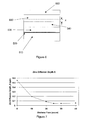
- Figure 7 shows the variation between the diffusion of zinc atoms and the disilane flow rate.
- the diffusion depth is indicated in Figure 6 and is the depth into the undoped InP layer 550 that zinc atoms have diffused.
- Figure 7 indicates that with no silicon doping the zinc atoms diffuse through almost the entire thickness of the undoped InP layer but that using a flow rate of 20 sccm or higher reduces the zinc diffusion to the first 50 nm of the undoped layer.
- the substrate 20 is n-type indium phosphide with a doping density of approximately 4 x 10 18 cm -3 (a preferred dopant is sulphur) which has a silicon doped oxide layer 90 formed on its upper surface. It is believed that the doped oxide layer has a thickness of approximately 20 ⁇ .
- a first cladding layer 30 of n-type InP with a thickness of approximately 1.5 ⁇ m and doping density of approximately 2.5 x 10 18 cm -3 is then grown on the doped oxide layer.
- the active region 40 comprises an undoped lower confinement layer of InGaAsP which is lattice matched to InP, an undoped InGaAsP strained MQW structure and an undoped upper confinement layer of InGaAsP which is lattice matched to InP.
- a second cladding layer 50 is then deposited upon the active region, having a thickness of approximately 0.4 ⁇ m and a doping density of approximately 1.4 x 10 18 cm -3 .
- oxide layers 95, 96 can be formed on the mesa sides after the etching step, rather than on the surface of the substrate.
- These oxide layers can be doped, with silicon for example, before the mesa overgrowth processes. Whilst these doped oxide layers will act as a barrier to reduce zinc diffusion from the subsequently formed blocking layers, they will not be able to reduce phosphorus diffusion from the substrate which is a cause of quantum well intermixing.
- Figure 8 shows a graphical depiction of an analysis of the semiconductor test structure of Figure 6 without use of the present invention.
- SIMS Secondary Ion Mass Spectrometry
- Figure 8 shows that the sulphur atoms are present in the upper cladding layer 560 and in the lower cladding layer 530 whilst there is an insignificant level of sulphur within the undoped layer.
- the zinc atoms are present in their greatest concentration within the p-type doped layer 540 and the undoped region 550.
- Figure 9 shows a similar analysis that has been performed on the semiconductor test structure shown in Figure 6.
- the analysis indicates that both silicon and oxygen are found at the interface between the substrate and the lower cladding layer (although the Si and O peaks appear to be overly broad as the oxide layer is believed to be only 20 ⁇ thick. This peak widening is believed to be an artefact of the SIMS analysis) .
- Figure 9 shows that the extent of zinc diffusion into the undoped region 550 has been reduced by the addition of the silicon-doped oxide layer.
- the doped oxide barriers present in the first two embodiments of the invention are both implemented within a single device.
- the silicon doped oxide could be deposited as a pattern using conventional photolithographic techniques with either an oxide or nitride mask. Once the silicon doped oxide has been formed, a thin layer of InP can be grown over the silicon doped oxide to allow the photolithographically defined mask to be stripped using hydrogen fluoride without damaging the doped oxide. This procedure would then allow selective intermixing of MQWs to provide a spatial variation of the MQW wavelength. This could enable the manufacture of a laser with an integral electro-absorption modulator, or of low-loss waveguides within an optoelectronic integrated circuit.
- Figure 10 shows a schematic depiction of a further embodiment of the present invention in which only selected areas of an InP substrate are doped and then oxidised. If a MQW structure is deposited above such a substrate and then annealed there will be differing levels of phosphorus diffusion from the substrate. The MQW structure above the undoped substrate regions will experience significant phosphorus diffusion, whilst the MQW structure above the doped substrate region will experience minimal phosphorus diffusion. The differing phosphorus densities in the different MQW areas will give rise to different levels of intermixing and thus different bandgap energy shifts; the greater the phosphorus density the greater the degree of intermixing and hence the greater the bandgap shift. This result can be exploited to form integrated semiconductor devices.
- An integrated laser-EAM could be formed by not doping the substrate oxide layer where the modulator is to be formed (leading to increased levels of intermixing) and doping the substrate oxide layer in the region where the laser is to be formed.
- low loss waveguides are required to connect the components. In this case the waveguides can be formed by causing regions on the wafer to become intermixed (by not providing any oxide on the substrate) in order to shift the bandgap energy, and hence the optical absorption edge, to reduce losses.
- semiconductor structure 210 comprises an indium phosphide substrate 220, first cladding layer 230, multiple quantum well region 240 and second cladding layer 250.
- Substrate 220 comprises oxidised doped regions 222, 224.
- the device is annealed under PH 3 /H 2 , for example at 800°C for 15 minutes. The annealing process causes phosphorus to diffuse from the substrate. Where the substrate does not comprise an oxidised doped region the phosphorus will migrate into the MQW structure and cause intermixing, causing the formation of areas 242 244 within the MQW region 240 in which there has been a significant bandgap shift. There will be a greatly reduced amount of intermixing in the rest of the MQW region 240, such that any bandgap shift would be much smaller.
- a preferred method by which selected areas of a substrate can be doped and then oxidised is to deposit a nitride or oxide mask onto the substrate and then remove the mask from regions where the oxidised doped region is to be formed using standard photolithographic techniques. Disilane can then be flowed over the heated substrate to cause the silicon doping and then the substrate can be oxidised. A layer of InP can then be deposited over the top of the doped oxide layer, for example somewhere between 10-200 nm thick, to protect it when the photolithographic mask is removed. After the mask has been removed, the epitaxial layers are deposited in a conventional manner and then the device is annealed.
- the device structure could be fabricated by depositing the dopant stabilised oxide over the entire surface of the substrate and then depositing an InP protective layer. Photolithographic techniques could then be used to selectively etch the indium phosphide and dopant stabilised oxide layers in order to obtain the desired patterning. This method is not preferred as there is a greater uncertainty in etch depth when compared with the method described above, leading to reduced process control and repeatability.
- the substrate could be chemically oxidised using nitric acid, again as long as the oxide layer is not significantly desorbed before layer growth occurs.
- the present invention is suitable for application with semiconductor lasers having a pnip blocking structure or to other InP-based devices that require minimal zinc diffusion to obtain adequate performance, such as heterojunction bipolar transistors.
- the present invention may also be applicable for use with other substrates, such as, for example, gallium arsenide.
Landscapes
- Physics & Mathematics (AREA)
- Engineering & Computer Science (AREA)
- Condensed Matter Physics & Semiconductors (AREA)
- General Physics & Mathematics (AREA)
- Optics & Photonics (AREA)
- Power Engineering (AREA)
- Microelectronics & Electronic Packaging (AREA)
- Computer Hardware Design (AREA)
- Manufacturing & Machinery (AREA)
- Chemical & Material Sciences (AREA)
- Electromagnetism (AREA)
- Nanotechnology (AREA)
- Geometry (AREA)
- Crystallography & Structural Chemistry (AREA)
- Biophysics (AREA)
- Life Sciences & Earth Sciences (AREA)
- Semiconductor Lasers (AREA)
Abstract
An oxide layer (90) on an indium phosphide semiconductor substrate
(20) is doped with silicon. This enables epitaxial layers to be
deposited upon the substrate in a conventional manner, including mesa
etching and overgrowth, to form a semiconductor structure (110). The
doped oxide layer is thought to reduce diffusion of phosphorus out of
the substrate and thus to reduce the zinc levels in the active region of
the structure. Additionally, or as an alternative, after mesa etching
oxide can be formed on the mesa sides and then doped with silicon.
Conventional blocking layers can then be formed over the doped oxide,
reducing the diffusion of zinc from the blocking layers into the
rest of the structure.
Description
This invention relates to the field of substrates used in
the manufacture of semiconductor devices and methods used
in the processing of such substrates.
Telecommunications equipment, and in particular equipment
for optical communication networks, have had significant
performance increases due to the use of III-V
semiconductor materials such as indium, phosphorus,
gallium and arsenic. As the performance of devices and
systems based upon III-V devices increases, new mechanisms
that interfere with the operation of the devices are
identified. It is the object of the present invention to
reduce the deleterious effect of one such mechanism within
indium phosphide (InP) devices.
According to a first aspect of the invention there is
provided a method of processing a semiconductor substrate,
the method comprising the steps of: forming a
semiconductor substrate comprising a III-V semiconductor
material; and depositing dopant material on one of the
surfaces of the semiconductor substrate; the method being
characterised by comprising the additional step of
oxidising said surface of the semiconductor substrate to
form an oxide layer comprising a significant concentration
of dopant material.
The dopant material may be selectively deposited on the
surface of the semiconductor substrate or the oxide layer
comprising a significant concentration of dopant material
may be selectively etched from the surface of the
semiconductor substrate. The dopant material may be
silicon and it may be deposited by flowing a gas over the
semiconductor substrate. The semiconductor substrate may
be oxidised by exposing the semiconductor substrate to an
oxidising agent.
According to a second aspect of the invention there is
provided a semiconductor substrate comprising: a
semiconductor layer comprising a III-V semiconductor
material; an oxide layer formed on one surface of the
semiconductor layer; characterised in that the oxide layer
comprises a significant concentration of dopant material.
The III-V semiconductor material may be indium phosphide
and it may be doped. The III-V semiconductor material may
be doped with an n-type dopant. The dopant material
deposited on the exterior surface of the semiconductor
substrate may be silicon.
According to a third aspect of the invention there is
provided a semiconductor device comprising a substrate and
a plurality of epitaxial semiconductor layers,
characterised in that the substrate comprises a III-V
semiconductor material and is in accordance with the
second aspect of the invention. Preferably the plurality
of epitaxial semiconductor layers comprise: a first
cladding layer formed upon the substrate; an active region
(40) formed upon the first cladding layer; and a second
cladding layer (50) formed upon the active region.
According to a fourth aspect of the invention there is
provided a method of manufacturing a semiconductor device,
the method comprising the steps of: (a) heating a
substrate comprising a layer of a III-V semiconductor
material to desorb a first oxide layer formed on a surface
of the substrate; and (b) depositing a plurality of
epitaxial layers of semiconductor material on the
substrate, the method being characterised by the
additional steps of: (I) depositing dopant material on one
of the surfaces of the semiconductor substrate; and (II)
oxidising the semiconductor substrate to form an oxide
layer comprising a significant concentration of dopant
material, steps (I) and (II) being performed after step
(a) and before step (b). Preferably wherein step (b)
comprises (i) depositing a first cladding layer on the
substrate; (ii) depositing an active region on the first
cladding layer; and depositing a second cladding layer on
the active region.
The method may comprise the additional step of: (d)
etching one or more of the plurality of epitaxial layers
of semiconductor material to form a mesa. Furthermore,
the method may include the step of: (e) depositing one or
more blocking layers of semiconductor material on the
sides of the mesa.
The method may also comprise the steps of: (f) depositing
dopant material on each side of the mesa; (g) oxidising
each side of the mesa to form oxide layers comprising a
significant concentration of dopant material; and (h)
depositing one or more blocking layers of semiconductor
material on the oxide layers. The method may comprise the
further step of: (i) depositing one or more further
epitaxial layers of semiconductor material on the
plurality of epitaxial layers deposited in step (b) and
the uppermost blocking layer.
The invention will now be described, by way of example
only, with reference to the following Figures in which:
Figure 1 shows an example of a known semiconductor
structure 10 that comprises an indium phosphide (InP)
substrate 20 that has an n-type dopant, a first InP
cladding layer 30 that has an n-type dopant, an undoped
indium gallium arsenide phosphide (InGaAsP) active layer
40 and a second InP cladding layer 50 that has a p-type
dopant. Such a structure may be used to manufacture a
semiconductor device such as, for example, a buried
heterostructure semiconductor laser.
Typically the structure 10 will be etched to form a mesa
(see Figure 2) before a overgrowth process is carried out,
in which the 'sides' of the mesa are 'filled in' with
blocking layers, and further layers are deposited on top
of the structure. Referring to Figure 3, first blocking
layers 60, 61 comprise indium phosphide with a p-type
dopant that each contain a second blocking layer 65, 66
that comprise indium-phosphide with an n-type dopant. The
first blocking layers are formed so as to be in contact
with the sides of the first and second cladding layers and
the active layer that were exposed through the etching
process and are grown to the same height as the second
cladding layer. The structure is completed by the
addition of a third cladding layer 70, which comprises
indium phosphide with a p-type dopant, and a contact layer
80 which comprises indium gallium arsenide (InGaAs) with a
p-type dopant.
The inventors believe that when the substrate is heated to
growth temperature, phosphorous atoms (or ions) are
released from lattice sites in the substrate and diffuse
up through the epitaxial structure of the device. When
they enter a zinc doped layer they cause the zinc atoms to
be released from lattice sites (although the mechanism by
which this happens is not fully understood). If the
phosphorus atoms (or ions) enter a MQW active region they
can induce intermixing (again, the mechanism for this is
not fully understood) and hence cause a shift in the
lasing wavelength. Additionally, when the zinc atoms are
released from their lattice sites they become mobile and
move through the semiconductor structure. If the mobile
zinc atoms enter the active region this can also cause a
wavelength shift (probably due to bandgap shrinkage).
Furthermore, the diffusion of zinc atoms into the first
and second cladding layers and the active layer of the
structure create further problems, such as poor device
performance at high temperatures, increased threshold
currents, shifts in the lasing wavelength, decreased
device reliability, etc.
Other potential p-type dopants, such as cadmium or
beryllium, are not as convenient to use as zinc in
semiconductor growth processes, nor are the dopants as
effective as zinc within the III-V structures.
Furthermore, it is believed that other p-type dopants
would diffuse in a similar manner to zinc and thus a
change of dopant would not be a solution to the present
problem.
There have been a number of proposed solutions to reduce
the levels of zinc diffusion, but they have not been
particularly effective and have had associated side
effects, such as reduced yield and poor device
performance. For example, US 5 771 256 discloses the
deposition of an AlInGaAs buffer layer between the
substrate and the epitaxial structure, which has proved to
be difficult to fabricate and only addresses the
wavelength shift that is caused by intermixing. Although
it is claimed that the AlInGaAs layer prevents wavelength
shift due to intermixing there is no indication that it
reduces or prevents zinc diffusion.
A further solution is the use of a substrate with a high
defect density, but this is not a preferred option as it
gives rise to undesirable reliability issues.
Conventionally, the substrate 10 will be supplied as a
wafer in a state that is referred to as "epi-ready", that
is ready for subsequent epitaxial growth. This means that
the surface will have been polished and then cleaned
before undergoing a controlled oxidation process such that
the substrate can be handled without being contaminated.
When the substrate wafer is subsequently processed in
order to form semiconductor devices, the initial heating
stage causes the oxide layer to desorb so that the
materials necessary to form the semiconductor device can
be deposited.
In the present invention the "epi-ready" substrate is
placed in a conventional reactor which is then heated up
to standard MOVPE (Metallo Organic Vapour Phase Epitaxy)
temperatures and the oxide layer is desorbed. The surface
of the substrate is doped using conventional techniques
and the substrate is then exposed to an oxidising agent
that forms an oxide layer on the substrate. The presence
of the silicon dopant increases the thermal stability of
the oxide layer. A dopant that has proved to work
successfully is silicon, the doping of which can be
achieved by flowing disilane (Si2H6) into the reactor at a
flow rate of 20 sccm (at a dilution of 50 vpm in argon),
for approximately 100 seconds. The substrate wafer is
allowed to cool to room temperature and is then briefly
exposed to the atmosphere to allow the doped surface to
oxidise. The wafer can then be returned to the reactor
for a semiconductor structure to be deposited in a
conventional manner. Referring to Figure 4, it can be
seen that a semiconductor structure 110 according to the
present invention is similar to the structure shown in
Figure 1 but additionally comprises a doped oxide layer 90
that is formed between the substrate 20 and the first
cladding layer 30. The structure of Figure 4 can be
etched to form a mesa and then re-grown in a conventional
manner.
It is understood that the doping of the oxide layer
stabilises the surface oxide layer, preventing the heating
effects of the reactor from desorbing all of the oxide
layer. It is also believed that the oxide layer acts as a
barrier layer and prevents phosphorus from diffusing out
of the substrate during the various temperature cycling
that occurs during the subsequent growth and etching
processes. This barrier effect is thought to reduce
subsequent zinc diffusion and quantum well intermixing.
Since the oxide layer is very thin, its presence is not
detrimental to the subsequent epitaxial growth or the
device characteristics.
Figure 6 shows an example of a semiconductor structure
that was deposited in order to determine the efficiency of
the present invention in reducing the diffusion of zinc
atoms within the structure. The substrate layer 510
comprises InP with an n-type dopant and the oxide layer
520 deposited on the substrate is silicon-doped in order
to increase its stability. A 0.5µm layer 530 of n-type
doped InP (doping density of 4 x 1018cm-3) is deposited on
the oxide layer, and then a 0.6µm layer 540 of p-type
doped InP (doping density of 1.5 x 1018cm-3) is applied. A
layer of undoped InP 550 (thickness 0.7µm) is applied with
a 0.5µm thick capping layer 560 of n-type doped InP
(doping density of 5 x 1018cm-3) being applied on top of
the undoped InP. The structure was annealed under
phosphine (PH3) for 90 minutes at a temperature of 625°C
(all layer thicknesses are pre-anneal values). A number
of these structures were produced, with a different flowrate
of disilane being used to dope the oxide layer of
each structure.
Figure 7 shows the variation between the diffusion of zinc
atoms and the disilane flow rate. The diffusion depth is
indicated in Figure 6 and is the depth into the undoped
InP layer 550 that zinc atoms have diffused. Figure 7
indicates that with no silicon doping the zinc atoms
diffuse through almost the entire thickness of the undoped
InP layer but that using a flow rate of 20 sccm or higher
reduces the zinc diffusion to the first 50 nm of the
undoped layer.
A semiconductor structure according to the present
invention is described with reference to Figure 4, purely
by way of example and it will be readily apparent that a
wide range of further structures can be realised using the
present invention. The substrate 20 is n-type indium
phosphide with a doping density of approximately 4 x
1018cm-3 (a preferred dopant is sulphur) which has a
silicon doped oxide layer 90 formed on its upper surface.
It is believed that the doped oxide layer has a thickness
of approximately 20Å. A first cladding layer 30 of n-type
InP with a thickness of approximately 1.5 µm and doping
density of approximately 2.5 x 1018cm-3 is then grown on the
doped oxide layer. The active region 40 comprises an
undoped lower confinement layer of InGaAsP which is
lattice matched to InP, an undoped InGaAsP strained MQW
structure and an undoped upper confinement layer of
InGaAsP which is lattice matched to InP. A second
cladding layer 50 is then deposited upon the active
region, having a thickness of approximately 0.4 µm and a
doping density of approximately 1.4 x 1018cm-3.
In a further embodiment of the present invention, which
will now be described with reference to Figure 5, oxide
layers 95, 96 can be formed on the mesa sides after the
etching step, rather than on the surface of the substrate.
These oxide layers can be doped, with silicon for example,
before the mesa overgrowth processes. Whilst these doped
oxide layers will act as a barrier to reduce zinc
diffusion from the subsequently formed blocking layers,
they will not be able to reduce phosphorus diffusion from
the substrate which is a cause of quantum well
intermixing.
Figure 8 shows a graphical depiction of an analysis of the
semiconductor test structure of Figure 6 without use of
the present invention. SIMS (Secondary Ion Mass
Spectrometry) has been used to determine the
concentration of sulphur and zinc species within the
structure. Figure 8 shows that the sulphur atoms are
present in the upper cladding layer 560 and in the lower
cladding layer 530 whilst there is an insignificant level
of sulphur within the undoped layer. In contrast, the
zinc atoms are present in their greatest concentration
within the p-type doped layer 540 and the undoped region
550.
Figure 9 shows a similar analysis that has been performed
on the semiconductor test structure shown in Figure 6. The
analysis indicates that both silicon and oxygen are found
at the interface between the substrate and the lower
cladding layer (although the Si and O peaks appear to be
overly broad as the oxide layer is believed to be only 20Å
thick. This peak widening is believed to be an artefact
of the SIMS analysis) . Figure 9 shows that the extent of
zinc diffusion into the undoped region 550 has been
reduced by the addition of the silicon-doped oxide layer.
In a third embodiment of the present invention, the doped
oxide barriers present in the first two embodiments of the
invention are both implemented within a single device.
In a fourth embodiment of the present invention, the
silicon doped oxide could be deposited as a pattern using
conventional photolithographic techniques with either an
oxide or nitride mask. Once the silicon doped oxide has
been formed, a thin layer of InP can be grown over the
silicon doped oxide to allow the photolithographically
defined mask to be stripped using hydrogen fluoride
without damaging the doped oxide. This procedure would
then allow selective intermixing of MQWs to provide a
spatial variation of the MQW wavelength. This could
enable the manufacture of a laser with an integral
electro-absorption modulator, or of low-loss waveguides
within an optoelectronic integrated circuit.
Figure 10 shows a schematic depiction of a further
embodiment of the present invention in which only selected
areas of an InP substrate are doped and then oxidised. If
a MQW structure is deposited above such a substrate and
then annealed there will be differing levels of phosphorus
diffusion from the substrate. The MQW structure above the
undoped substrate regions will experience significant
phosphorus diffusion, whilst the MQW structure above the
doped substrate region will experience minimal phosphorus
diffusion. The differing phosphorus densities in the
different MQW areas will give rise to different levels of
intermixing and thus different bandgap energy shifts; the
greater the phosphorus density the greater the degree of
intermixing and hence the greater the bandgap shift. This
result can be exploited to form integrated semiconductor
devices. In order to form a laser with an integrated
electro-absorption modulator (EAM) it is necessary to form
active regions having different bandgap energies on the
same wafer. An integrated laser-EAM could be formed by
not doping the substrate oxide layer where the modulator
is to be formed (leading to increased levels of
intermixing) and doping the substrate oxide layer in the
region where the laser is to be formed. Similarly in
order to make an optoelectronic integrated circuit low
loss waveguides are required to connect the components. In
this case the waveguides can be formed by causing regions
on the wafer to become intermixed (by not providing any
oxide on the substrate) in order to shift the bandgap
energy, and hence the optical absorption edge, to reduce
losses.
Referring to Figure 10, semiconductor structure 210
comprises an indium phosphide substrate 220, first
cladding layer 230, multiple quantum well region 240 and
second cladding layer 250. Substrate 220 comprises
oxidised doped regions 222, 224. Once all of the
epitaxial layers have been formed the device is annealed
under PH3/H2, for example at 800°C for 15 minutes. The
annealing process causes phosphorus to diffuse from the
substrate. Where the substrate does not comprise an
oxidised doped region the phosphorus will migrate into the
MQW structure and cause intermixing, causing the formation
of areas 242 244 within the MQW region 240 in which there
has been a significant bandgap shift. There will be a
greatly reduced amount of intermixing in the rest of the
MQW region 240, such that any bandgap shift would be much
smaller.
A preferred method by which selected areas of a substrate
can be doped and then oxidised is to deposit a nitride or
oxide mask onto the substrate and then remove the mask
from regions where the oxidised doped region is to be
formed using standard photolithographic techniques.
Disilane can then be flowed over the heated substrate to
cause the silicon doping and then the substrate can be
oxidised. A layer of InP can then be deposited over the
top of the doped oxide layer, for example somewhere
between 10-200 nm thick, to protect it when the
photolithographic mask is removed. After the mask has been
removed, the epitaxial layers are deposited in a
conventional manner and then the device is annealed.
In an alternative, the device structure could be
fabricated by depositing the dopant stabilised oxide over
the entire surface of the substrate and then depositing an
InP protective layer. Photolithographic techniques could
then be used to selectively etch the indium phosphide and
dopant stabilised oxide layers in order to obtain the
desired patterning. This method is not preferred as there
is a greater uncertainty in etch depth when compared with
the method described above, leading to reduced process
control and repeatability.
It will be understood that materials other than silicon
could be used to stabilise the oxide layer. The inventor
has obtained the same effect using iron in place of
silicon and it is believed that the invention can be
implemented using other commonly used dopants for example
tin, zinc, carbon, aluminium, sulphur, etc., and that
those who are skilled in the art of semiconductor
fabrication technology would readily understand the
materials and processes required to use such dopants.
Additionally, it is been demonstrated that it is possible
to thermally oxidise the substrate in flowing oxygen,
although the beneficial results are lost if the oxide
layer is not sufficiently thick and/or stable such that
the layer desorbs before growth is commenced. As a
further alternative, the substrate could be chemically
oxidised using nitric acid, again as long as the oxide
layer is not significantly desorbed before layer growth
occurs.
In addition to the laser devices described above and
similar devices, the present invention is suitable for
application with semiconductor lasers having a pnip
blocking structure or to other InP-based devices that
require minimal zinc diffusion to obtain adequate
performance, such as heterojunction bipolar transistors.
Although the preceding discussion has focussed on the use
of doping to stabilise an oxide layer that has been
deposited on an indium phosphide substrate, the present
invention may also be applicable for use with other
substrates, such as, for example, gallium arsenide.
Claims (20)
- A method of processing a semiconductor substrate, the method comprising the steps of:forming a semiconductor substrate (20) comprising a III-V semiconductor material; anddepositing dopant material on one of the surfaces of the semiconductor substrate (20);the method being characterised by comprising the additional step of oxidising said surface of the semiconductor substrate (20) to form an oxide layer (90) comprising a significant concentration of dopant material.
- A method according to claim 1 wherein the dopant material is selectively deposited on the surface of the semiconductor substrate (20).
- A method according to claim 1 wherein the oxide layer (90) comprising a significant concentration of dopant material is selectively etched from the surface of the semiconductor substrate.
- A method according to any preceding claim wherein the dopant material is silicon.
- A method according to any preceding claim wherein the dopant material is deposited by flowing a gas over the semiconductor substrate (20).
- A method according to any preceding claim wherein the semiconductor substrate (20) is oxidised by exposing the semiconductor substrate (20) to an oxidising agent.
- A semiconductor substrate comprising:characterised in that the oxide layer comprises a significant concentration of dopant material.a semiconductor layer (20) comprising a III-V semiconductor material;an oxide layer (90) formed on one surface of the semiconductor layer;
- A semiconductor substrate according to claim 7 wherein the III-V semiconductor material is indium phosphide.
- A semiconductor substrate according to claim 7 or claim 8 wherein the III-V semiconductor material that comprises the semiconductor layer is doped.
- A semiconductor substrate according to claim 9 wherein the III-V semiconductor material that comprises the semiconductor layer is doped with an n-type dopant.
- A semiconductor substrate according to claim 10 wherein the III-V semiconductor material that comprises the semiconductor layer is doped with sulphur.
- A semiconductor substrate according to any of claims 7 to 11 wherein the dopant material deposited on the exterior surface of the semiconductor substrate (20) is silicon.
- A semiconductor device (10) comprising a substrate (20) and a plurality of epitaxial semiconductor layers, (30,40, 50) characterised in that the substrate comprises a III-V semiconductor material and is in accordance with any of claims 7 to 12.
- A semiconductor device according to claim 13, wherein the plurality of epitaxial semiconductor layers comprise:a first cladding layer (30) formed upon the substrate (20);an active region (40) formed upon the first cladding layer (30); anda second cladding layer (50) formed upon the active region (40).
- A method of manufacturing a semiconductor device, the method comprising the steps of:(a) heating a substrate (20) comprising a layer of a III-V semiconductor material to desorb a first oxide layer formed on a surface of the substrate; and(b) depositing a plurality of epitaxial layers (30, 40, 50) of semiconductor material on the substrate, the method being characterised by the additional steps of:(I) depositing dopant material on one of the surfaces of the semiconductor substrate (20); and(II) oxidising the semiconductor substrate (20) to form an oxide layer (90) comprising a significant concentration of dopant material, steps (I) and (II) being performed after step (a) and before step (b).
- A method of manufacturing a semiconductor device according to claim 15, wherein step (b) comprises(i) depositing a first cladding layer (30) on the substrate (20);(ii) depositing an active region (40) on the first cladding layer (30); and(iii) depositing a second cladding layer (50) on the active region (40).
- A method of manufacturing a semiconductor device according to claim 15 or claim 16, the method comprising the additional step of:(d) etching one or more of the plurality of epitaxial layers of semiconductor material to form a mesa.
- A method of manufacturing a semiconductor device according to claim 17, the method comprising the additional step of:(e) depositing one or more blocking layers (60, 61, 65, 66) of semiconductor material on the sides of the mesa.
- A method of manufacturing a semiconductor device according to claim 17, the method comprising the additional steps of:(f) depositing dopant material on each side of the mesa;(g) oxidising each side of the mesa to oxide layers (95, 96) comprising a significant concentration of dopant material; and(h) depositing one or more blocking layers (60, 61, 65, 66) of semiconductor material on the oxide layers.
- A method of manufacturing a semiconductor device according to claim 18 or claim 19, the method comprising the additional step of:(i) depositing one or more further epitaxial layers (70, 80) of semiconductor material on the plurality of epitaxial layers deposited in step (b) and the uppermost blocking layer.
Priority Applications (3)
| Application Number | Priority Date | Filing Date | Title |
|---|---|---|---|
| EP02253129A EP1359614A1 (en) | 2002-05-02 | 2002-05-02 | Semiconductor substrates and structures with an oxide layer |
| JP2003115193A JP2004006826A (en) | 2002-05-02 | 2003-04-21 | Semiconductor device |
| US10/423,149 US6818925B2 (en) | 2002-05-02 | 2003-04-25 | Semiconductor substrates and structures |
Applications Claiming Priority (1)
| Application Number | Priority Date | Filing Date | Title |
|---|---|---|---|
| EP02253129A EP1359614A1 (en) | 2002-05-02 | 2002-05-02 | Semiconductor substrates and structures with an oxide layer |
Publications (1)
| Publication Number | Publication Date |
|---|---|
| EP1359614A1 true EP1359614A1 (en) | 2003-11-05 |
Family
ID=28799738
Family Applications (1)
| Application Number | Title | Priority Date | Filing Date |
|---|---|---|---|
| EP02253129A Withdrawn EP1359614A1 (en) | 2002-05-02 | 2002-05-02 | Semiconductor substrates and structures with an oxide layer |
Country Status (3)
| Country | Link |
|---|---|
| US (1) | US6818925B2 (en) |
| EP (1) | EP1359614A1 (en) |
| JP (1) | JP2004006826A (en) |
Families Citing this family (2)
| Publication number | Priority date | Publication date | Assignee | Title |
|---|---|---|---|---|
| JP2009135333A (en) * | 2007-11-30 | 2009-06-18 | Sumitomo Electric Ind Ltd | Method for manufacturing for semiconductor light-emitting element |
| US20210257463A1 (en) * | 2018-06-20 | 2021-08-19 | Lawrence Livermore National Security, Llc | Field assisted interfacial diffusion doping through heterostructure design |
Citations (5)
| Publication number | Priority date | Publication date | Assignee | Title |
|---|---|---|---|---|
| US4914059A (en) * | 1986-10-27 | 1990-04-03 | Yves Nissim | Process for the heat flash vapour phase deposition of an insulating layer on a III-V material substrate and its application to the production of a MIS structure |
| EP0814549A2 (en) * | 1996-06-20 | 1997-12-29 | Nec Corporation | Semiconductor laser |
| US5719891A (en) * | 1995-12-18 | 1998-02-17 | Picolight Incorporated | Conductive element with lateral oxidation barrier |
| US5945690A (en) * | 1993-11-09 | 1999-08-31 | Fujitsu Limited | Compound semiconductor device |
| EP1083642A2 (en) * | 1999-09-09 | 2001-03-14 | Hitachi, Ltd. | Broad band semiconductor optical amplifier and optical communication system |
Family Cites Families (3)
| Publication number | Priority date | Publication date | Assignee | Title |
|---|---|---|---|---|
| FR2593966B1 (en) * | 1986-02-04 | 1988-09-09 | Ankri David | MONOLITHIC SEMICONDUCTOR STRUCTURE OF A HETEROJUNCTION BIPOLAR TRANSISTOR AND A LASER |
| FR2743196B1 (en) * | 1995-12-27 | 1998-02-06 | Alsthom Cge Alcatel | METHOD FOR MANUFACTURING A SURFACE EMITTING SEMICONDUCTOR LASER |
| US6392257B1 (en) * | 2000-02-10 | 2002-05-21 | Motorola Inc. | Semiconductor structure, semiconductor device, communicating device, integrated circuit, and process for fabricating the same |
-
2002
- 2002-05-02 EP EP02253129A patent/EP1359614A1/en not_active Withdrawn
-
2003
- 2003-04-21 JP JP2003115193A patent/JP2004006826A/en active Pending
- 2003-04-25 US US10/423,149 patent/US6818925B2/en not_active Expired - Fee Related
Patent Citations (5)
| Publication number | Priority date | Publication date | Assignee | Title |
|---|---|---|---|---|
| US4914059A (en) * | 1986-10-27 | 1990-04-03 | Yves Nissim | Process for the heat flash vapour phase deposition of an insulating layer on a III-V material substrate and its application to the production of a MIS structure |
| US5945690A (en) * | 1993-11-09 | 1999-08-31 | Fujitsu Limited | Compound semiconductor device |
| US5719891A (en) * | 1995-12-18 | 1998-02-17 | Picolight Incorporated | Conductive element with lateral oxidation barrier |
| EP0814549A2 (en) * | 1996-06-20 | 1997-12-29 | Nec Corporation | Semiconductor laser |
| EP1083642A2 (en) * | 1999-09-09 | 2001-03-14 | Hitachi, Ltd. | Broad band semiconductor optical amplifier and optical communication system |
Also Published As
| Publication number | Publication date |
|---|---|
| JP2004006826A (en) | 2004-01-08 |
| US6818925B2 (en) | 2004-11-16 |
| US20030205716A1 (en) | 2003-11-06 |
Similar Documents
| Publication | Publication Date | Title |
|---|---|---|
| US6653248B2 (en) | Doped semiconductor material, a method of manufacturing the doped semiconductor material, and a semiconductor device | |
| US20020175344A1 (en) | Enhancement of carrier concentration in As-containing contact layers | |
| JP2686764B2 (en) | Method for manufacturing optical semiconductor device | |
| US8039282B2 (en) | Semiconductor optical device and method of fabricating the same | |
| JPH06296060A (en) | Manufacture of visible light semiconductor laser diode | |
| JP4260480B2 (en) | Method of manufacturing an optical device and related improvements | |
| US20210288471A1 (en) | Vertical-Cavity Surface-Emitting Device with Epitaxial Index Guide | |
| US7682857B2 (en) | Method for manufacturing semiconductor optical device | |
| US6818925B2 (en) | Semiconductor substrates and structures | |
| US7456040B2 (en) | Method for producing semiconductor optical device | |
| KR100766027B1 (en) | Photo device epilayer structure of lattice-matched InGaAs/InGaAsP multiple-quantum-well structure by high-energy ion implantation and method for fabricating the same | |
| JPH09214045A (en) | Semiconductor laser and its fabrication method | |
| JPH07202317A (en) | Manufacture of embedded structure semiconductor laser | |
| JP4210741B2 (en) | Method for manufacturing an optical device | |
| JP2000031596A (en) | Semiconductor laser and its manufacture | |
| US6229836B1 (en) | Semiconductor laser and a method of manufacturing therefor | |
| EP1193771A2 (en) | Method for fabricating a semiconductor device | |
| US7138285B2 (en) | Control of contact resistance in quantum well intermixed devices | |
| US7449723B2 (en) | Semiconductor device | |
| JP3213428B2 (en) | Semiconductor laser device and method of manufacturing the same | |
| CN115395366A (en) | Method for manufacturing laser chip | |
| KR100596510B1 (en) | Fabricating method of semiconductor optical element | |
| JPH10294526A (en) | Manufacture of semiconductor device, and semiconductor device | |
| GB2323708A (en) | A method of fabricating a semiconductor layer | |
| KR19980084824A (en) | Semiconductor laser diode and manufacturing method thereof |
Legal Events
| Date | Code | Title | Description |
|---|---|---|---|
| PUAI | Public reference made under article 153(3) epc to a published international application that has entered the european phase |
Free format text: ORIGINAL CODE: 0009012 |
|
| AK | Designated contracting states |
Kind code of ref document: A1 Designated state(s): AT BE CH CY DE DK ES FI FR GB GR IE IT LI LU MC NL PT SE TR |
|
| AX | Request for extension of the european patent |
Extension state: AL LT LV MK RO SI |
|
| 17P | Request for examination filed |
Effective date: 20040506 |
|
| AKX | Designation fees paid |
Designated state(s): DE GB |
|
| 17Q | First examination report despatched |
Effective date: 20040709 |
|
| STAA | Information on the status of an ep patent application or granted ep patent |
Free format text: STATUS: THE APPLICATION IS DEEMED TO BE WITHDRAWN |
|
| 18D | Application deemed to be withdrawn |
Effective date: 20041130 |