EP1359612A2 - Methods of manufacturing a hybrid integrated circuit device - Google Patents
Methods of manufacturing a hybrid integrated circuit device Download PDFInfo
- Publication number
- EP1359612A2 EP1359612A2 EP03009358A EP03009358A EP1359612A2 EP 1359612 A2 EP1359612 A2 EP 1359612A2 EP 03009358 A EP03009358 A EP 03009358A EP 03009358 A EP03009358 A EP 03009358A EP 1359612 A2 EP1359612 A2 EP 1359612A2
- Authority
- EP
- European Patent Office
- Prior art keywords
- substrate
- grooves
- metal substrate
- circuit
- hybrid integrated
- Prior art date
- Legal status (The legal status is an assumption and is not a legal conclusion. Google has not performed a legal analysis and makes no representation as to the accuracy of the status listed.)
- Withdrawn
Links
Images










Classifications
-
- H—ELECTRICITY
- H10—SEMICONDUCTOR DEVICES; ELECTRIC SOLID-STATE DEVICES NOT OTHERWISE PROVIDED FOR
- H10W—GENERIC PACKAGES, INTERCONNECTIONS, CONNECTORS OR OTHER CONSTRUCTIONAL DETAILS OF DEVICES COVERED BY CLASS H10
- H10W99/00—Subject matter not provided for in other groups of this subclass
-
- H—ELECTRICITY
- H05—ELECTRIC TECHNIQUES NOT OTHERWISE PROVIDED FOR
- H05K—PRINTED CIRCUITS; CASINGS OR CONSTRUCTIONAL DETAILS OF ELECTRIC APPARATUS; MANUFACTURE OF ASSEMBLAGES OF ELECTRICAL COMPONENTS
- H05K3/00—Apparatus or processes for manufacturing printed circuits
- H05K3/0011—Working of insulating substrates or insulating layers
- H05K3/0044—Mechanical working of the substrate, e.g. drilling or punching
- H05K3/0052—Depaneling, i.e. dividing a panel into circuit boards; Working of the edges of circuit boards
-
- H—ELECTRICITY
- H10—SEMICONDUCTOR DEVICES; ELECTRIC SOLID-STATE DEVICES NOT OTHERWISE PROVIDED FOR
- H10W—GENERIC PACKAGES, INTERCONNECTIONS, CONNECTORS OR OTHER CONSTRUCTIONAL DETAILS OF DEVICES COVERED BY CLASS H10
- H10W70/00—Package substrates; Interposers; Redistribution layers [RDL]
- H10W70/01—Manufacture or treatment
- H10W70/02—Manufacture or treatment of conductive package substrates serving as an interconnection, e.g. of metal plates
- H10W70/027—Mechanical treatments, e.g. deforming, punching or cutting
-
- H—ELECTRICITY
- H10—SEMICONDUCTOR DEVICES; ELECTRIC SOLID-STATE DEVICES NOT OTHERWISE PROVIDED FOR
- H10W—GENERIC PACKAGES, INTERCONNECTIONS, CONNECTORS OR OTHER CONSTRUCTIONAL DETAILS OF DEVICES COVERED BY CLASS H10
- H10W90/00—Package configurations
-
- H—ELECTRICITY
- H05—ELECTRIC TECHNIQUES NOT OTHERWISE PROVIDED FOR
- H05K—PRINTED CIRCUITS; CASINGS OR CONSTRUCTIONAL DETAILS OF ELECTRIC APPARATUS; MANUFACTURE OF ASSEMBLAGES OF ELECTRICAL COMPONENTS
- H05K1/00—Printed circuits
- H05K1/02—Details
- H05K1/03—Use of materials for the substrate
- H05K1/05—Insulated conductive substrates, e.g. insulated metal substrate
- H05K1/056—Insulated conductive substrates, e.g. insulated metal substrate the metal substrate being covered by an organic insulating layer
-
- H—ELECTRICITY
- H05—ELECTRIC TECHNIQUES NOT OTHERWISE PROVIDED FOR
- H05K—PRINTED CIRCUITS; CASINGS OR CONSTRUCTIONAL DETAILS OF ELECTRIC APPARATUS; MANUFACTURE OF ASSEMBLAGES OF ELECTRICAL COMPONENTS
- H05K2201/00—Indexing scheme relating to printed circuits covered by H05K1/00
- H05K2201/09—Shape and layout
- H05K2201/09009—Substrate related
- H05K2201/09036—Recesses or grooves in insulating substrate
-
- H—ELECTRICITY
- H05—ELECTRIC TECHNIQUES NOT OTHERWISE PROVIDED FOR
- H05K—PRINTED CIRCUITS; CASINGS OR CONSTRUCTIONAL DETAILS OF ELECTRIC APPARATUS; MANUFACTURE OF ASSEMBLAGES OF ELECTRICAL COMPONENTS
- H05K2201/00—Indexing scheme relating to printed circuits covered by H05K1/00
- H05K2201/09—Shape and layout
- H05K2201/09009—Substrate related
- H05K2201/0909—Preformed cutting or breaking line
-
- H—ELECTRICITY
- H05—ELECTRIC TECHNIQUES NOT OTHERWISE PROVIDED FOR
- H05K—PRINTED CIRCUITS; CASINGS OR CONSTRUCTIONAL DETAILS OF ELECTRIC APPARATUS; MANUFACTURE OF ASSEMBLAGES OF ELECTRICAL COMPONENTS
- H05K2201/00—Indexing scheme relating to printed circuits covered by H05K1/00
- H05K2201/09—Shape and layout
- H05K2201/09209—Shape and layout details of conductors
- H05K2201/09654—Shape and layout details of conductors covering at least two types of conductors provided for in H05K2201/09218 - H05K2201/095
- H05K2201/09745—Recess in conductor, e.g. in pad or in metallic substrate
-
- H—ELECTRICITY
- H05—ELECTRIC TECHNIQUES NOT OTHERWISE PROVIDED FOR
- H05K—PRINTED CIRCUITS; CASINGS OR CONSTRUCTIONAL DETAILS OF ELECTRIC APPARATUS; MANUFACTURE OF ASSEMBLAGES OF ELECTRICAL COMPONENTS
- H05K2203/00—Indexing scheme relating to apparatus or processes for manufacturing printed circuits covered by H05K3/00
- H05K2203/02—Details related to mechanical or acoustic processing, e.g. drilling, punching, cutting, using ultrasound
- H05K2203/0228—Cutting, sawing, milling or shearing
-
- H—ELECTRICITY
- H05—ELECTRIC TECHNIQUES NOT OTHERWISE PROVIDED FOR
- H05K—PRINTED CIRCUITS; CASINGS OR CONSTRUCTIONAL DETAILS OF ELECTRIC APPARATUS; MANUFACTURE OF ASSEMBLAGES OF ELECTRICAL COMPONENTS
- H05K2203/00—Indexing scheme relating to apparatus or processes for manufacturing printed circuits covered by H05K3/00
- H05K2203/15—Position of the PCB during processing
- H05K2203/1572—Processing both sides of a PCB by the same process; Providing a similar arrangement of components on both sides; Making interlayer connections from two sides
-
- H—ELECTRICITY
- H05—ELECTRIC TECHNIQUES NOT OTHERWISE PROVIDED FOR
- H05K—PRINTED CIRCUITS; CASINGS OR CONSTRUCTIONAL DETAILS OF ELECTRIC APPARATUS; MANUFACTURE OF ASSEMBLAGES OF ELECTRICAL COMPONENTS
- H05K2203/00—Indexing scheme relating to apparatus or processes for manufacturing printed circuits covered by H05K3/00
- H05K2203/30—Details of processes not otherwise provided for in H05K2203/01 - H05K2203/17
- H05K2203/302—Bending a rigid substrate; Breaking rigid substrates by bending
-
- H—ELECTRICITY
- H05—ELECTRIC TECHNIQUES NOT OTHERWISE PROVIDED FOR
- H05K—PRINTED CIRCUITS; CASINGS OR CONSTRUCTIONAL DETAILS OF ELECTRIC APPARATUS; MANUFACTURE OF ASSEMBLAGES OF ELECTRICAL COMPONENTS
- H05K3/00—Apparatus or processes for manufacturing printed circuits
- H05K3/22—Secondary treatment of printed circuits
- H05K3/28—Applying non-metallic protective coatings
- H05K3/284—Applying non-metallic protective coatings for encapsulating mounted components
-
- H—ELECTRICITY
- H10—SEMICONDUCTOR DEVICES; ELECTRIC SOLID-STATE DEVICES NOT OTHERWISE PROVIDED FOR
- H10W—GENERIC PACKAGES, INTERCONNECTIONS, CONNECTORS OR OTHER CONSTRUCTIONAL DETAILS OF DEVICES COVERED BY CLASS H10
- H10W72/00—Interconnections or connectors in packages
- H10W72/01—Manufacture or treatment
- H10W72/0198—Manufacture or treatment batch processes
-
- H—ELECTRICITY
- H10—SEMICONDUCTOR DEVICES; ELECTRIC SOLID-STATE DEVICES NOT OTHERWISE PROVIDED FOR
- H10W—GENERIC PACKAGES, INTERCONNECTIONS, CONNECTORS OR OTHER CONSTRUCTIONAL DETAILS OF DEVICES COVERED BY CLASS H10
- H10W72/00—Interconnections or connectors in packages
- H10W72/851—Dispositions of multiple connectors or interconnections
- H10W72/874—On different surfaces
- H10W72/884—Die-attach connectors and bond wires
-
- H—ELECTRICITY
- H10—SEMICONDUCTOR DEVICES; ELECTRIC SOLID-STATE DEVICES NOT OTHERWISE PROVIDED FOR
- H10W—GENERIC PACKAGES, INTERCONNECTIONS, CONNECTORS OR OTHER CONSTRUCTIONAL DETAILS OF DEVICES COVERED BY CLASS H10
- H10W90/00—Package configurations
- H10W90/701—Package configurations characterised by the relative positions of pads or connectors relative to package parts
- H10W90/731—Package configurations characterised by the relative positions of pads or connectors relative to package parts of die-attach connectors
- H10W90/734—Package configurations characterised by the relative positions of pads or connectors relative to package parts of die-attach connectors between a chip and a stacked insulating package substrate, interposer or RDL
-
- H—ELECTRICITY
- H10—SEMICONDUCTOR DEVICES; ELECTRIC SOLID-STATE DEVICES NOT OTHERWISE PROVIDED FOR
- H10W—GENERIC PACKAGES, INTERCONNECTIONS, CONNECTORS OR OTHER CONSTRUCTIONAL DETAILS OF DEVICES COVERED BY CLASS H10
- H10W90/00—Package configurations
- H10W90/701—Package configurations characterised by the relative positions of pads or connectors relative to package parts
- H10W90/751—Package configurations characterised by the relative positions of pads or connectors relative to package parts of bond wires
- H10W90/754—Package configurations characterised by the relative positions of pads or connectors relative to package parts of bond wires between a chip and a stacked insulating package substrate, interposer or RDL
Definitions
- the present invention pertains generally to integrated circuit devices and preferred embodiments pertain generally to methods for manufacturing a hybrid integrated circuit device and, more particularly, to a hybrid integrated circuit device manufacturing method with which a plurality of circuit substrates are manufactured by dicing from a single, large-size metal substrate.
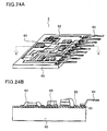
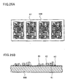
- Fig. 24(A) is a perspective view of a hybrid integrated circuit device 6.
- Fig. 24(B) is a sectional view taken along the line X-X' of Fig. 24(A).
- the existing hybrid integrated circuit device 6 has the following arrangement.
- the hybrid integrated circuit device 6 includes a rectangular substrate 60, a conductive pattern 62 formed on an insulating layer 61 that is disposed on the top surface of substrate 60, circuit elements 63 affixed onto the conductive pattern 62, metal wires 65 which electrically connect circuit elements 63 with the conductive pattern 62, and leads 64 which are electrically connected with the conductive pattern.
- the hybrid integrated circuit device 6 is completed as a product by sealing the hybrid integrated circuit formed on the top surface of circuit substrate 60 with an insulating resin or a case material, etc.
- FIG. 25(A) is a plan view of large-size metal substrate 66A
- Fig. 25(B) is a sectional view of large-size metal substrate 66A.
- a method of partitioning large-size metal substrate 66A into elongate parts will be described with reference to Fig. 25(A). As shown in FIG. 25(A), a large-size metal substrate 66A is partitioned into elongated parts along lines D4.
- a metal substrate 66A shall now be described with reference to Fig. 25(B).
- the substrate 66A is formed of aluminum and both of its surfaces have been subjected to an alumite treatment.
- an insulating layer 61 for the insulation of the metal substrate 66A with respect to a conductive pattern, is provided on the surface on which a hybrid integrated circuit is to be formed.
- a copper foil 68 which becomes a conductive pattern 62 (shown in Fig. 26(B)), is press bonded to insulating layer 61.
- FIG. 26(A) is plan view of an elongated metal substrate 66B on which a plurality of hybrid integrated circuits 67 have been formed.
- Fig. 26(B) is a sectional view of Fig. 26(A).
- conductive patterns 62 are formed by etching copper foil 68 that has been press bonded onto insulating layer 61.
- conductive patterns 62 are etched so as to form a plurality of hybrid integrated circuits on the elongated metal substrate 66B.
- a resin overcoat is applied above the conductive patterns 62 in order to protect conductive patterns 62.
- Solder or brazing material is then used to affix circuit elements 63 onto predetermined locations on each conductive pattern 62.
- Passive elements and active elements may be employed generally as circuit elements 63.
- the transistor is mounted onto a heat sink that is affixed to the conductive pattern.
- a method of partitioning the metal substrate 66B, on which a plurality of hybrid integrated circuits 67 have been formed, into individual circuit substrates 60 shall now be described with reference to Fig. 27.
- individual circuit substrates 60 each having a hybrid integrated circuit 67 formed on a top surface, are partitioned from metal substrate 66B by punching out parts of the circuit substrate 60 using a press.
- the press punches out the metal substrate 66B from the surfaces on which hybrid integrated circuits 67 are formed.
- margins are provided around the peripheral end parts of circuit substrate 60, where margins conductive patterns 62 and circuit elements 63 are not formed.
- the substrates are then completed as products by a step of sealing the hybrid integrated circuit 67, etc.
- the insulating layer 61 is formed on the top surface of metal substrate 66B, which insulating layer 61 is extremely hard since it is highly filled with alumina.
- the blade edge of the press for performing "punching" can wear quickly.
- productivity is lowered because an expert worker is needed to carry out the process of exchanging the blade edge of a press and because the exchange of the blade edge requires a very large amount of time.
- a main object of this invention is to provide a method of manufacturing a hybrid integrated circuit device with which a plurality of circuit substrates are manufactured from a single, large-size metal substrate by dicing which lessens these drawbacks.
- a method of manufacturing a hybrid integrated circuit device includes: preparing a metal substrate having an insulating layer over a top surface; forming conductive patterns over the insulating layer; forming a lattice of grooves in a rear surface of the metal substrate; mounting a hybrid integrated circuit over at least one of the conductive patterns; and separating individual circuit substrates with a rotatable cutter contacting the metal substrate at locations corresponding to the grooves to cut remaining thicknesses of the metal substrate and the insulating layer.
- the rotatable cutter is a circular cutter that rotates without an external drive.
- the rotatable cutter is a rotatable saw.
- the grooves have a generally V-shaped cross-section and a depth of the grooves is shallower than a thickness of the metal substrate.
- the metal substrate is formed of a material principally comprising aluminum or copper.
- the metal substrate is an aluminum substrate, wherein top and rear surfaces of the aluminum substrate have been subject to alumite treatment.
- the insulating layer is a resin filled with aluminum.
- a method of manufacturing a hybrid integrated circuit device includes: preparing a metal substrate having an insulating layer over a top surface; forming a plurality of conductive patterns over a top surface of the insulating layer; forming lattices of grooves in the top and rear surfaces of the metal substrate; mounting a hybrid integrated circuit on at least one of the conductive patterns; and separating the metal substrate along the grooves into individual circuit substrates.
- the separating includes bending the metal substrate at the locations where the grooves were formed to separate the metal substrate into the individual circuit substrates.
- the separating includes separating individual circuit substrates with a rotatable cutter contacting the metal substrate at locations corresponding to the grooves to cut remaining thicknesses of the metal substrate and the insulating layer.
- the forming lattices of grooves includes using a cutting saw, with blade edges of a shape corresponding to a cross-section of the grooves, that is rotated at a high speed to form the grooves.
- the blade edges of the saw are substantially flat.
- a method of manufacturing an integrated circuit device includes: preparing a substrate having an insulating layer; forming a plurality of conductive patterns over the insulating layer; forming a plurality of grooves in at least one of a top or a bottom surface of the substrate; and separating the metal substrate along the grooves into individual circuit substrates.
- the integrated circuit device is a hybrid integrated circuit device and the substrate is a metal substrate.
- grooves are formed in both the top and bottom surface.
- the grooves in the bottom surface are deeper than the grooves in the top surface.
- the individual circuit substrates are formed with peripheral sides having inclined parts.
- the method further includes sealing the individual circuit substrates in an insulating resin, such as, e.g., by transfer molding.
- such inclined parts are configured to inhibit entry of resin beneath the substrate during sealing.
- the individual circuit substrates are formed with the conductive patterns very near at least one peripheral end, such as, e.g., within about 2 mm of at least one peripheral end, or within about 1 mm of at least one peripheral end.
- the invention allows to achieve one or more of the following advantages.
- the mounting of, e.g., a few dozen to a few hundred hybrid integrated circuits on a single metal substrate is enabled.
- the etching step, die bonding step, and wire bonding step can thus be performed as batch processes. The productivity can thereby be improved.
- a circular cutter without a driving force can be rotated by pressing it against the metal substrate and the metal substrate can be partitioned thereby. Since the remaining thickness parts at grooves and insulating layer can thus be cut by the circular cutter, cutting chips will not be generated. The short-circuiting of the hybrid integrated circuits in the manufacturing process can thus be prevented.
- the metal substrate can be partitioned by pressing a circular cutter against parts corresponding to grooves.
- the lowering of the voltage resistance of the devices due to the generation of cracks in the resin layer can thus be prevented.
- the flatness of substrate can be secured.
- circuit substrates are separated by "cutting" a metal substrate using a saw or a circular cutter.
- different blades needed to be prepared in accordance with the sizes of the circuit substrates to be manufactured can be accommodated by simply changing the dicing lines.
- a plurality of hybrid integrated circuits are mounted in matrix form on a single metal substrate. Since the respective hybrid integrated circuits are very close to each other, substantially the entire surface of the metal substrate becomes circuit substrates. The waste loss of material can thus be reduced.
- first grooves and second grooves are formed in a lattice form on the top surface and rear surface of metal substrate, circuit substrates can be partitioned readily at the locations where the grooves are formed. Methods of partitioning by bending and circular cutter may be considered for the partitioning of the respective circuit substrates and partitioning can be performed readily by using either method.
- FIG. 1(A) is a perspective view of a hybrid integrated circuit device 1.
- Fig. 1(B) is a sectional view taken along the line X-X' of Fig. 1(A).
- hybrid integrated circuit device 1 The structure of hybrid integrated circuit device 1, according to this illustrative embodiment, shall now be described with reference to Figs. 1(A)-(B).
- the hybrid integrated circuit device 1 is preferably sealed in resin as shown.
- an insulating resin 16 preferably has a function of sealing the hybrid integrated circuit, including, for example, circuit elements 13, etc., that are disposed on a top surface of a circuit substrate 10.
- any appropriate resin may be employed, such as, by way of example only, a thermoplastic resin (e.g., which seals upon being injection molded), a thermosetting resin (e.g., which seals upon being transfer molded) and/or other appropriate materials may be employed.
- a side face of circuit substrate 10 preferably has a vertical part 10A and an inclined part 10B.
- an angle formed between the top surface and the vertical part 10A of circuit substrate 10 is or is approximately a right angle.
- an angle formed between the bottom surface and the inclined part 10B of circuit substrate 10 is preferably an obtuse angle as shown.
- the angle can be substantially the same as that depicted in the Figures (all of the appended Figures being to scale in some illustrative and non-limiting embodiments). In this manner, when resin sealing is applied with the bottom surface of circuit substrate 10 exposed as in the Fig.
- insulating resin 16 can set around the inclined parts 10B. In this manner, the insulating resin can create an anchor effect between inclined parts 10B and the insulating resin 16.
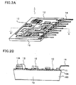
- Fig. 2(A) is a perspective view of hybrid integrated circuit device 1 and Fig. 2(B) is a sectional view along line X-X' of Fig. 2(A).
- the hybrid integrated circuit device 1 preferably includes a circuit substrate 10 (formed, e.g., of a metal), an insulating layer 11 (formed, e.g., on a top surface of circuit substrate 10), a conductive pattern 12 (formed, e.g., on the insulating layer 11), circuit elements 13 (mounted, e.g., to predetermined positions on conductive pattern 12), etc.
- a circuit substrate 10 formed, e.g., of a metal
- an insulating layer 11 formed, e.g., on a top surface of circuit substrate 10
- a conductive pattern 12 formed, e.g., on the insulating layer 11
- circuit elements 13 mounted, e.g., to predetermined positions on conductive pattern 12
- circuit substrate 10 aluminum, copper and/or another metal is used for the material of the circuit substrate 10.
- an alloy can be used for the material of circuit substrate 10.
- any appropriate materials known to those in the art may be employed.
- a circuit substrate 10 that is formed of aluminum is employed.
- both surfaces of the substrate have been subjected to an alumite treatment.
- a side face of circuit substrate 10 is formed with a vertical part 10A that extends vertically from the top surface and an inclined part 10B that inclines towards an inner side of the circuit substrate 10 as it extends downwards from vertical part 10A. While, in some embodiments, the vertical part 10A can be oriented in or substantially in an exactly vertical orientation, in this disclosure, the terminology vertical or vertical part does not signify an exactly vertical orientation, but also encompasses generally vertical orientations.
- the inclined parts 10B are formed on the side faces of circuit substrate 10 during the manufacturing method.
- the circuit substrate 10 is manufactured by cutting and dividing a large-size substrate.
- V-shaped or generally V-shaped grooves are preferably formed in a rear surface of the large-size substrate.
- the remaining thicknesses of the substrate above the V-shaped grooves are preferably removed starting from, preferably, the top surface.
- the sides of the V-shaped groove parts become the inclined parts 10B of the individual substrates.
- Insulating layer 11 is preferably formed on a top surface of circuit substrate 10.
- the insulating layer has a function of insulating the conductive pattern 12 and the circuit substrate.
- the insulating layer 11 is also highly filled with, for example, alumina for actively transferring heat generated from, e.g., circuit elements 13 to the circuit substrate 10.
- the conductive pattern 12 is preferably disposed on a top surface of insulating layer 11. Preferably, it is formed with copper and/or another metal. In the preferred embodiments, the conductive pattern 12 is formed across substantially the entire or the entire top surface of circuit substrate 10. In this regard, in preferred embodiments, the conductive pattern 12 is formed near one or more peripheral ends of the circuit substrate. In some embodiments, the conductive pattern extends to within 2 mm from one or more peripheral ends of circuit substrate 10. In some embodiments, the conductive pattern extends to within 1 mm from one or more peripheral ends of circuit substrate 10, or even less than 1 mm in other embodiments.
- the conductive pattern 12 can be formed near the peripheral end parts of the circuit substrate 10 because of the method used in the partitioning of the circuit substrate 10. While some preferred methods of partitioning circuit substrate 10 shall be described in detail below, generally speaking, individual circuit substrates 10 are preferably separated from a large-size substrate by partitioning the metal substrate in a unique manner (e.g., with a cutter). In the related art example described above, margins near the peripheral end parts of circuit substrate 10 were required because the circuit substrates were partitioned by a press. On the other hand, preferred embodiments herein enable the margins to be eliminated and a conductive pattern 12 to be formed over substantially the entire or the entire top surface of circuit substrate 10.
- circuit elements 13 are mounted by solder or brazing material onto predetermined locations of conductive pattern 12.
- passive elements and/or active elements can be employed generally as circuit elements 13.
- the transistor is preferably mounted onto a heat sink that is affixed to the conductive pattern.
- a circuit element 13 can be positioned at substantially any location upon the circuit substrate 10. That is, a circuit element 13 can be positioned near a peripheral end part of circuit substrate 10. For example, a circuit element can be positioned on the top surface of circuit substrate within about 2 mm from a peripheral end part of circuit substrate 10, or within about 1 mm from a peripheral end part of a circuit substrate, or even less.
- a heat sink 13A is mounted to a predetermined location of conductive pattern 12.
- a power transistor can be mounted on a top surface of this heat sink and the power transistor can be electrically connected with conductive pattern 12 by, e.g., metal wires 15.
- the heat sink 13A can now be positioned at subtantially any location on the circuit substrate 10. Specifically, heat sink 13A can be positioned even near a peripheral end part within, e.g., about 2 mm from a peripheral end of circuit substrate 10, or even less.
- the heat sink 13 can be formed up to near the peripheral end parts of circuit substrate 10 because of the preferred methods of partitioning the circuit substrate 10 according to the present invention.
- circuit substrate 10 are preferably separated from a large-size substrate by partitioning the metal substrate in a unique manner.
- margins near the peripheral end parts of circuit substrate 10 were required because the circuit substrates were partitioned by a press.
- a heat sink 13 onto which a power transistor is mounted had the greatest height among the circuit elements 13, it could not be positioned at a peripheral part of circuit substrate 10.
- the preferred embodiments of the present invention enable the margins to be eliminated and enable, e.g., a heat sink 13A to be mounted at substantially any location on the top surface of circuit substrate 10. In various embodiments, this same substantially-any-location benefit can be made available to passive elements, active elements and/or any other circuit elements 13.
- leads 14 are affixed to pads formed of conductive pattern 12 and have a function of performing input and output with respect to the exterior.
- a power transistor, etc. can be mounted face-up and electrically connected with the conductive pattern 12 by, e.g., metal wires 15.
- an overcoat of resin, etc. can be applied to locations of the conductive pattern 12 where an electrical connection is not made.
- the arrangement of hybrid integrated circuit device 10 described above provides one or more, preferably all, of the following effects.
- the conductive pattern 12 can be formed up to near the end parts of the circuit substrate 10, in cases where the same circuit as that of another existing example is formed, the size of the entire hybrid integrated circuit device can be made small.
- the circuit elements 13 can be positioned up to near the end parts of circuit substrate 10, the degree of freedom in designing the electrical circuit can be improved. Furthermore, since the density of the pattern can be improved, in cases where the same circuit as that of an existing related art example is formed, the size of the entire hybrid integrated circuit device can be reduced.
- the parts where the side faces of circuit substrate 10 continue to the rear surface are formed to have an obtuse angle without a rounded shape.
- insulating resin 16 in a step of using a mold die for sealing in insulating resin 16 with the rear surface of the circuit substrate being exposed, insulating resin 16 can be prevented from entering into gaps between the mold die and the circuit substrate 10. Insulating resin 16 can thus be prevented from becoming attached to the rear surface of circuit substrate 10.
- the corner between the rear surface of the substrate 10 and the inclined part 10B is not rounded in a manner that may facilitate resin flow therearound.
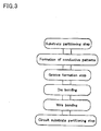
- a hybrid integrated circuit device is preferably manufactured using at least some, preferably all, of the following steps: cutting and dividing a large-size substrate (e.g., a metal substrate) into mid-size substrates by partitioning the large-size substrate; forming conductive patterns of a plurality of hybrid integrated circuits on a top surface of each mid-size substrate; forming grooves in a lattice form on a surface of each mid-size substrate on which an insulating layer is not provided; performing die bonding to mount circuit elements onto the conductive patterns; performing wire bonding; separating individual circuit substrates by cutting the remaining thickness parts at the grooves of the substrate and the insulating layer, etc. Then, the separated circuit substrates 10 are preferably sealed in an insulating resin.
- a large-size substrate e.g., a metal substrate
- forming conductive patterns of a plurality of hybrid integrated circuits on a top surface of each mid-size substrate
- forming grooves in a lattice form on a surface of each mid
- a large-size metal substrate 10A' is preferably partitioned to form mid-size metal substrates 10B'.
- a large-size metal substrate 10A' can be prepared as shown in Fig. 4(A).
- the size of large-size substrate 10A' can be, for example, approximately 1 m 2 (1 square meter) or more. However, the size of the substrate 10A' can vary based on circumstances.
- the substrate 10A' can be an aluminum substrate, both surfaces of which have been subject to alumite treatment.
- an insulating layer is provided on the top surface of metal substrate 10A'.
- a copper foil, which is to become conductive patterns, is preferably formed on the top surface of the insulating layer.
- the metal substrate 10A' is partitioned along dicing lines D1 by a cutter 31.
- the cutter 31 includes a rotary saw.
- various other cutters can be used in other embodiments, such as, e.g., knives, blades, scizzors, guillotines, shears, reciprocated cutters, rotary cutters and/or various other cutters (see, e.g., other embodiments discussed below).
- a plurality of sheets of metal substrates 10A' can be overlapped and partitioned simultaneously.
- the saw 31 partitions the metal substrate 10A' along dicing lines D1 while rotating at a high speed.
- dicing line is used to identify the locations along which the partitioning is to be effected and does not necessarily require physical lines or features to be present on the substrate.
- a large-size metal substrate 10A' with a generally square shape is partitioned into eight parts along dicing lines D1 and made into elongated mid-sized metal substrates 10B'.
- the shape of a mid-sized metal substrate 10B' is such that the length of the long side is about twice the length of the short side.
- a rotary saw having features as shown in Fig. 4(C) is provided.
- a preferred shape, etc., of a blade edge of a saw 31 is shown in Fig. 4(C).
- Fig. 4(C) is an enlarged view of the vicinity of a blade edge 31A of the saw 31.
- the end part of blade edge 31A is formed to be flat.
- a diamond material is embedded therein.
- etching can be performed on a mid-sized metal substrate 10B' manufactured by this step to remove the copper foil partially and thereby form conductive patterns.
- the number of conductive patterns depends on the size of metal substrate 10B' and the size of a hybrid integrated circuit, conductive patterns that form, for example, several dozen to several hundred hybrid integrated circuits can be formed on a single metal substrate 10B'.
- Fig. 5(A) is a plan view of an illustrative mid-sized metal substrate 10 that had been partitioned in a prior step.
- Fig. 5(B) is a perspective view, showing an illustrative condition in which grooves can be formed in the substrate 10A' using a V-cut saw 35.
- Fig. 5(C) is an enlarged view of a blade edge 35A of the blade 35 shown in Fig. 5(B).
- a V-cut saw 35 can be rotated at a high speed to form grooves in the metal substrate along dicing lines D2.
- the dicing lines D2 are situated in a lattice form.
- the dicing lines D2 correspond to boundary lines of individual conductive patterns formed on insulating layer 11. While in the illustrated embodiment, a single cutter, e.g., saw 35, is depicted, various embodiments can employ a plurality of cutters, if desired.
- Fig. 5(C) is an enlarged view of the vicinity of a blade edge 35A of the saw 35 illustrating a preferred shape of the V-cut saw 35.
- the V-cut saw 35 is preferably provided with a plurality of blade edges 35A having a shape substantially as shown.
- the shape of a blade edge 35A corresponds to a shape of a groove to be provided in the metal substrate 10A'.
- grooves with a V-shaped cross section are formed on the rear surface of the metal substrate (e.g., a surface on which insulating layer 11 is not provided).
- the shape of a blade edge 35A is preferably also substantially a V-shape.
- a diamond material is embedded in blade edge 35A.
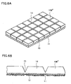
- Fig. 6(A) is a perspective view of the metal substrate 10B' with which grooves have been formed by V-cut saw 35 and Fig. 6(B) is a sectional view of metal substrate 10B'.
- grooves 20 are preferably formed in a lattice form on the surface of metal substrate 10B' on which insulating layer 11 is not provided.
- the grooves are formed using a V-cut saw 35 having substantially V-shaped blade edges 35A, the grooves 20 are formed to have a substantially V-shaped cross-section.
- the central lines of grooves 20 e.g., at an apex of the "V" correspond to the boundary lines of the individual conductive patterns 12 formed on insulating layer 11.
- a groove 20 is preferably formed to have a substantially V-shaped cross section.
- the depth of groove 20 is preferably made shallower than the thickness of metal substrate 10B'.
- the metal substrate 10B' is not partitioned into individual circuit substrates 10. That is, the individual circuit substrates 10 are connected at the remaining thickness parts of the metal substrate 10B' that correspond to the groove 20 parts.
- the metal substrate 10B' can be handled as a single, sheet-like object.
- the "burrs" are formed in this step, the "burrs" are removed, such as, e.g., by performing high-pressure washing.
- the circuit elements 13 are preferably mounted onto conductive patterns 12 and electrical connections are made between the circuit elements 13 and the conductive patterns 12.
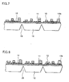
- Fig. 7 is a sectional view showing a condition in which circuit elements 13 have been mounted onto conductive patterns 12.
- the circuit elements 13 are mounted onto predetermined locations of conductive patterns 12 by, for example, soft solder or other soldering material.
- conductive patterns 12 are preferably formed near the peripheral end parts of circuit substrates 10.
- the circuit elements 13 can thus also be mounted near the peripheral end parts of circuit substrates 10.
- a heat sink 13A on the upper surface of which a power tansistor is mounted, is a circuit element that is typically higher in height in comparison to other circuit elements.
- a heat sink 13A could not be positioned near a peripheral end part of a circuit substrate.
- the circuit substrates 10 can be partitioned individually using, e.g., a circular cutter.
- a heat sink 13A and/or another circuit element 13 with increased height can even be positioned near a peripheral end part of a circuit substrate.
- Fig. 8 is a sectional view showing a condition where circuit elements 13 are electrically connected with conductive pattern 12 by metal wires 15.
- wire bonding is preferably performed in a batch process on, for example, several dozen to several hundred hybrid integrated circuits formed on a single substrate 10B'.
- Fig. 9 is a plan view of a part of hybrid integrated circuits 17 formed on metal substrate 10B'. In preferred embodiments, as depicted by the wavy line edges, an even greater number of hybrid integrated circuits 17 are preferably formed.
- the substrate 10B' can be partitioned into individual circuit substrates 10 along dicing lines D3.
- the conductive patterns 12 that form the individual hybrid integrated circuits can be formed very close to the dicing lines D3. In this manner, the conductive patterns 12 can be formed over substantially the entire or the entire the top surface of the substrate 10B'.
- heat sinks 13A and other circuit elements 13 can also be disposed at peripheral parts of the hybrid integrated circuits.
- hybrid integrated circuits were formed in a batch on a top surface of a substrate 10B' having an elongated shape.
- the substrate 10B' can be partitioned into desired sizes in a step prior to the present step.
- a metal substrate having a square shape can be obtained by partitioning the metal substrate 10B' in two pieces in a step prior to the present step.
- Fig. 10(A) is a perspective view, showing the condition where a metal substrate 10B' is partitioned into individual circuit substrates 10 using a circular cutter 41.
- Fig. 10(B) is a sectional view of Fig. 10(A).
- a plurality of hybrid integrated circuits can be already formed on insulating layer 11.
- circular cutter 41 is preferably used in this illustrative embodiment to force-cut the metal substrate 10B' along the dicing lines D3.
- the metal substrate 10B' can thereby be partitioned into individual circuit substrates 10.
- the circular cutter 41 preferably force-cuts the surface of metal substrate 10, on which insulating layer 11 is provided, at parts corresponding to the central lines (e.g., along the apexes) of the grooves 20.
- each groove 20 has a substantially V-shaped cross section. In this manner, the circular cutter 41 can cut the remaining thickness parts of the metal substrate 10B' and the insulating layer 11 at parts where grooves 20 have been formed most deeply (e.g., the deepest parts of the grooves).
- the circular cutter 41 preferably has the shape of a circular disk.
- the peripheral edge part is formed into an acute angle.
- the central part of circular cutter 41 is fixed to a supporting part 42 in a manner enabling free rotation of circular cutter 41 (such as, e.g., so as to rotate about a central axis).
- the circular cutter 41 is preferably not driven by a driving force.
- the circular cutter 41 freely rotates such that it rotates as it is moved along a dicing line D3 while a part of circular cutter 41 is pressed against metal substrate 10B' (e.g., due to the contact therebetween).
- a radius of circular cutter 41 (e.g., h2 plus d) is preferably set longer than the length obtained by adding d1 and h1.
- a heat sink 13A and/or another circuit element 13 with some height can be positioned at a peripheral part of circuit substrate 10.
- the position of a heat sink 13A may thus be close to a dicing line D3 as shown in Fig. 10.
- the position of a supporting part 42 can be set so that supporting part 42 will not contact the heat sink 13A in such a case.
- the length h2 from the lower end of supporting part 42 to the top surface of insulating layer 11, is preferably set longer than h1.
- the supporting part 42 is shown as having a lower end proximate a central axis of the cutter 41, the lower end can have a dissimilar position in other embodiments.
- the top part of a metal wire 15 extending from, e.g., a power transistor that is mounted to a heat sink 13A is the highest part within the hybrid integrated circuit.
- the lower end of supporting part 42 is preferably set at a position that is higher than the top part of metal wire 15.
- FIG. 11 is a sectional view, showing the step of sealing circuit substrate 10 in an insulating resin 16 by use of, e.g., a mold die 50.
- circuit substrate 10 is preferably set on a lower mold die 50B.
- Insulating resin 16 can then be injected through a gate 53.
- transfer molding using a thermosetting resin or injection molding using a thermosetting resin can be employed as the method of sealing. Air of an amount corresponding to the amount of the insulating resin 16 that is injected from gate 53 can be ejected from the interior of the cavity to the exterior via an air vent 54.
- inclined parts 10B are preferably provided at side face parts of circuit substrate 10.
- insulating resin 16 is set around the vicinity of inclined part 10B.
- an anchor effect is provided between the insulating resin 16 and the inclined part 10B and the joining of insulating resin 16 and circuit substrate 10 can be, thereby, fortified.
- the cross-sectional shape of the part where the rear surface of circuit substrate 10 continues to an inclined part 10B is formed to have an obtuse angle.
- the inclined part 10B is not rounded at its bottom end adjacent the rear surface of the substrate so that insulating resin 16, which is injected through the gate 53 into the cavity, is limited from entry beneath the substrate (e.g., between the rear surface of the substrate and the lower mold die 50B).
- the inclined part 10B can have substantially any configuration in various embodiments (e.g., straight, arcuate, rounded, convex, concave, irregular, etc.), in preferred embodiments it is configured to inhibit entry of resin beneath the substrate (such as, e.g., not having rounded edges and/or not otherwise configuring the inclined part 10B such that resin may enter therebehind).
- the circuit substrate 10 which has been sealed in resin in the above-described step, can be completed as a product upon being subject to, for example, a lead cutting step, etc.
- the foregoing embodiments can provide one or more, preferably all, of the following effects.
- the exchange of saw 31 can be a comparatively simple task and can be performed quickly.
- the work efficiency can be improved in comparison to the related art case where a shearing blade needs to be exchanged.
- grooves are formed at parts of metal substrate 10B' that correspond to the boundaries of the individual circuit substrates 10.
- the thinned parts corresponding to the grooves 20 will bend first, while the remaining portions can remain substantially unbent. Accordingly, degradation of the flatness of the individual circuit substrates 10 can thus be inhibited.
- the mounting of, for example, a few dozen to a few hundred hybrid integrated circuits on a single metal substrate 10B' is enabled.
- the etching step, die bonding step, and wire bonding step can thus be performed as batch processes. The productivity can thereby be improved.
- a circular cutter 41 without a driving force can be rotated by pressing it against metal substrate 10B' so as to partition the metal substrate 10B'.
- cutting chips will be virtually eliminated. Accordingly, short-circuiting of the hybrid integrated circuits in the manufacturing process can thus be prevented.
- the metal substrate 10B' can be partitioned by pressing a circular cutter 41 against regions corresponding to grooves 20 (such as, e.g., at regions above the grooves).
- regions corresponding to grooves 20 such as, e.g., at regions above the grooves.
- the lowering of the voltage resistance of the devices due to generation of cracks in resin layer 11 can thus be prevented.
- the flatness of substrate 10B' can be secured.
- individual circuit substrates can be separated by "cutting" a metal substrate using, e.g., a cutter, such as, for example, a cutter saw 31 or a circular cutter 41.
- a cutter such as, for example, a cutter saw 31 or a circular cutter 41.
- different blades needed to be prepared in accordance with the sizes of the circuit substrates to be manufactured can be accommodated by simply changing the dicing lines (i.e., by changing locations along which the cutters are moved).
- the cutters can be moved via various moving means, such as, by way of example only, a robot arm that can be controlled via a controller (e.g., to control movement, path of movement, etc.) and/or other means.
- a plurality of hybrid integrated circuits can be mounted in a matrix form on a single metal substrate 10B'. Since the respective hybrid integrated circuits can be very close to each other, substantially the entire surface of metal substrate 10B' can be made into circuit substrates 10. As a result, the waste loss of material can be substantially diminished.
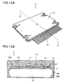
- FIG. 12(A) is a perspective view of a hybrid integrated circuit device 1 and Fig. 12(B) is a sectional view along line X-X' of Fig. 12(A).
- hybrid integrated circuit device 1 The preferred structure of hybrid integrated circuit device 1 shall now be described with reference to Figs. 12(A)-(B).
- the illustrative hybrid integrated circuit device 1 shown in these Figures is sealed in a resin.
- Insulating resin 16 preferably has a function of sealing a hybrid integrated circuit, including circuit elements 13, etc., that are disposed on the top surface of a circuit substrate 10.
- a thermoplastic resin which seals upon being injection molded
- a thermosetting resin which seals upon being transfer molded, etc.
- a side face of circuit substrate 10 preferably has a vertical part 10A and an inclined part 10B.
- the angle formed by the rear surface and inclined part 10B of circuit substrate 10 is an obtuse angle.
- the insulating resin 16 is preferably set around inclined parts 10B.
- an anchor effect can be provided between inclined parts 10B and the insulating resin 16.
- upper inclined parts 10B are also formed along the side faces above the vertical part 10A and continuing toward the top surface of circuit substrate 10.
- Fig. 13(A) is a perspective view of hybrid integrated circuit device 1 and Fig. 13(B) is a sectional view along line X-X' of Fig. 13(A).
- an illustrative hybrid integrated circuit device 1 can have the following arrangement.
- the hybrid integrated circuit device 1 preferably includes, e.g., a circuit substrate 10 (formed of, e.g., a metal), an insulating layer 11 (formed, e.g., on a top surface of circuit substrate 10), a conductive pattern 12 (formed, e.g., on an insulating layer 11), circuit elements 13 (mounted, e.g., to predetermined positions on conductive pattern 12), etc.
- a circuit substrate 10 formed of, e.g., a metal
- an insulating layer 11 formed, e.g., on a top surface of circuit substrate 10
- a conductive pattern 12 formed, e.g., on an insulating layer 11
- circuit elements 13 mounted, e.g., to predetermined positions on conductive pattern 12
- circuit substrate 10 In preferred embodiments, aluminum, copper and/or another metal is used for the material of the circuit substrate 10. In some embodiments, an alloy can be used for the material of circuit substrate 10. In various embodiments, any appropriate materials known to those in the art may be employed. In some preferred embodiments, a circuit substrate 10 that is formed of aluminum is employed. Preferably, both surfaces of the substrate have been subjected to an alumite treatment. In some illustrative embodiments, a side face of circuit substrate 10 is formed with inclined parts 10B that incline from the upper surface and the lower surface, respectively, and a vertical part 10A that extends between the inclined parts 10B.
- the inclined parts 10B are formed on the side faces of the circuit substrate 10 during the manufacturing method.
- the circuit substrate 10 is manufactured by cutting and dividing a large-size substrate.
- V-shaped or generally V-shaped grooves are preferably formed from the top surface and the rear surface of the substrate.
- the remaining thicknesses of the substrate above the V-shaped grooves are preferably removed starting from, preferably, the top surface.
- These V-shaped groove parts become the inclined parts 10B.
- Insulating layer 11 is preferably formed on the top surface of circuit substrate 10.
- the insulating layer has a function of insulating the conductive pattern 12 and the circuit substrate.
- the insulating layer 11 is also highly filled with alumina for actively transferring the heat generated from circuit elements 13 to the circuit substrate 10.
- the conductive pattern 12 is preferably disposed on the top surface of insulating layer 11. Preferably, it is formed with copper and/or another metal. In the preferred embodiments, the conductive pattern 12 is formed across substantially the entire or the entire top surface of circuit substrate 10. In some embodiments, the conductive pattern 12 is formed near one or more peripheral end parts of the circuit substrate. In some embodiments, the conductive pattern extends to within about 2 mm from one or more peripheral ends of circuit substrate 10. In some embodiments, the conductive pattern extends to within about 1 mm from one or more peripheral ends of circuit substrate 10, or even less than 1 mm in other embodiments.
- the conductive pattern 12 can be formed near the peripheral end parts of the circuit substrate 10 because of the method used in the partitioning of the circuit substrate 10. While some preferred methods of partitioning circuit substrate 10 shall be described in detail below, generally speaking, individual circuit substrates 10 are preferably separated from a large-size substrate by partitioning the metal substrate in a unique manner (e.g., with a cutter). In the related art example described above, margins near the peripheral end parts of circuit substrate 10 were required because the circuit substrates were partitioned by a press. On the other hand, preferred embodiments herein enable the margins to be eliminated and a conductive pattern 12 to be formed over substantially the entire or the entire top surface of circuit substrate 10.
- circuit elements 13 are mounted by solder or brazing material onto predetermined locations of conductive pattern 12.
- passive elements and/or active elements can be employed generally as circuit elements 13.
- the transistor is preferably mounted onto a heat sink that is affixed to the conductive pattern.
- a circuit element 13 can be positioned at substantially any location upon the circuit substrate 10. That is, a circuit element 13 can be positioned near a peripheral end part of circuit substrate 10. For example, a circuit element can be positioned on the top surface of circuit substrate within about 2 mm from a peripheral end part of circuit substrate 10, or within about 1 mm from a peripheral end part of a circuit substrate, or even less.
- a heat sink 13A is mounted to a predetermined location of conductive pattern 12.
- a power transistor can be mounted on a top surface of this heat sink and the power transistor can be electrically connected with conductive pattern 12 by, e.g., metal wires 15.
- the heat sink 13A can be positioned at substantially any location of circuit substrate 10. Specifically, heat sink 13A can be positioned even near a peripheral end part within, e.g., about 2 mm from a peripheral end of circuit substrate 10, or even less. Once again, the heat sink 13 can be formed up to near the peripheral end parts of circuit substrate 10 because of the preferred methods of partitioning the circuit substrate 10 according to the preferred embodiments.
- circuit substrate 10 are preferably separated from a large-size substrate by partitioning the metal substrate in a unique manner.
- margins near the peripheral end parts of circuit substrate 10 were required because the circuit substrates were partitioned by a press.
- a heat sink 13 onto which a power transistor is mounted had the greatest height among the circuit elements 13, it could not be positioned at a peripheral part of circuit substrate 10.
- the preferred embodiments of the present invention enable the margins to be eliminated and enable, e.g., a heat sink 13A to be mounted at substantially any location on the top surface of circuit substrate 10. In various embodiments, this same substantially-any-location benefit can be made available to passive elements, active elements and/or any other circuit elements 13.
- leads 14 are affixed to pads formed of conductive pattern 12 and have a function of performing input and output with respect to the exterior.
- a power transistor, etc. can be mounted face-up and electrically connected with the conductive pattern 12 by, e.g., metal wires 15.
- an overcoat of resin, etc. can be applied to locations of the conductive pattern 12 where an electrical connection is not made.
- the arrangement of hybrid integrated circuit device 10 described above provides one or more, preferably all, of the following effects.
- conductive pattern 12 can be formed up to near the end parts of circuit substrate 10, in cases where the same circuit as that of a prior-art example is formed, the size of the entire hybrid integrated circuit device can be made small.
- the circuit elements 13 can be positioned up to near the end parts of circuit substrate 10, the degree of freedom in designing the electrical circuit can be improved. Furthermore, since the density of the pattern can be improved, in cases where the same circuit as that of an existing related art example is formed, the size of the entire hybrid integrated circuit device can be reduced.
- the parts where the side faces of circuit substrate 10 continue to the rear surface are formed to have an obtuse angle without a rounded shape.
- insulating resin 16 in a step of using a mold die for sealing in insulating resin 16 with the rear surface of the circuit substrate being exposed, insulating resin 16 can be prevented from entering into gaps between the mold die and the circuit substrate 10. Insulating resin 16 can thus be prevented from becoming attached to the rear surface of circuit substrate 10.
- the corner between the rear surface of the substrate 10 and the inclined part 10B is not rounded in a manner that may facilitate resin flow therearound.
- a hybrid integrated circuit device manufacturing method can include at least some, preferably all, of the following steps: preparing a metal substrate 10A' having an insulating layer 11 formed on a top surface thereof; forming a plurality of conductive patterns 12 on the top surface of insulating layer 11; forming grooves 20 in a lattice form on a top surface and a rear surface of the metal substrate 10B'; mounting hybrid integrated circuits onto conductive patterns 12; and separating individual circuit substrates 10 by separating the metal substrate 10B' at the locations where grooves 20 are formed.
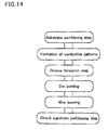
- a hybrid integrated circuit device is preferably manufactured by the following steps. That is, a hybrid integrated circuit device is preferably manufactured using at least some, preferably all, of the following steps: cutting and dividing a large-size substrate 10A' (e.g., a metal substrate) into mid-size substrates 10B' by partitioning the large-size substrate 10A'; forming conductive patterns 12 of a plurality of hybrid integrated circuits on a top surface of each mid-size substrate 10B'; forming first grooves 20A and second grooves 20B in lattice form on the top surface and the rear surface of each mid-size substrate 10B'; performing die bonding to mount circuit elements 13 onto conductive patterns 12; performing wire bonding; separating individual circuit substrates 10 by partitioning metal substrate 10B' at locations where grooves 20A/20B have been formed, etc. Then, the partitioned circuit substrates 10 are preferably sealed in an insulating resin.
- the preferred embodiment are preferably sealed in an insulating resin.
- a large-size substrate 10A' is preferably partitioned to form mid-size metal substrates 10B'.
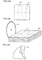
- a large-size metal substrate 10A' can be prepared as shown in Fig. 15(A).
- the size of large-size substrate 10A' can be, for example, approximately 1 m 2 (1 square meter) or more. However, the size of the substrate 10A' can vary based on circumstances.
- the substrate 10A' can be an aluminum substrate, both surfaces of which have been subject to alumite treatment.
- an insulating layer is provided on the top surface of metal substrate 10A'.
- a copper foil, which is to become conductive patterns, is preferably formed on the top surface of the insulating layer.
- the metal substrate 10A' is partitioned along dicing lines D1 by a cutter 31.
- the cutter 31 includes a rotary saw.
- various other cutters can be used in other embodiments, such as, e.g., knives, blades, scizzors, guillotines, shears, reciprocated cutters, rotary cutters, and/or various other cutters.
- a plurality of sheets of metal substrate 10A' can be overlapped and partitioned simultaneously.
- the saw 31 partitions metal substrate 10A' along dicing lines D1 while rotating at high speed.
- a large-size metal substrate 10A' with a generally square shape is partitioned into eight parts along dicing lines D1 and made into elongated mid-sized metal substrates 10B'.
- the shape of a mid-sized metal substrate 10B' is such that the length of the long side is about twice the length of the short side.
- a rotary saw having features as shown in Fig. 15(C) is provided.
- a preferred shape, etc., of a blade edge of a saw 31 is shown in Fig. 15(C).
- Fig. 15(C) is an enlarged view of the vicinity of a blade edge 31A of the saw 31.
- the end part of blade edge 31A is formed to be flat.
- a diamond material is embedded therein.
- etching can be performed on a mid-sized metal substrate 10B' manufactured by this step to remove the copper foil partially and thereby form conductive patterns.
- the number of conductive patterns depends on the size of metal substrate 10B' and the size of a hybrid integrated circuit, conductive patterns that form, for example, several dozen to several hundred hybrid integrated circuits can be formed on a single metal substrate 10B'.
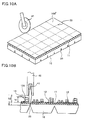
- first grooves 20A and second grooves 20B are preferably formed in lattice form on the top and rear surfaces of the mid-sized metal substrate 10B'.
- Fig. 16(A) is a plan view of a mid-sized metal substrate 10B' that had been partitioned in a prior step.
- Fig. 16(B) is a perspective view, showing an illustrative condition in which grooves can be formed in the substrate 10A' using a V-cut saw 35.
- Fig. 16(C) is an enlarged view of blade edge 35A of the blade 35 shown in FIG. 16(B).
- a V-cut saw 35 can be rotated at a high speed to form first grooves 20A and second grooves 20B in the top surface and rear surface of the metal substrate along dicing lines D2.
- the dicing lines D2 are situated in a lattice form.
- the dicing lines D2 correspond to boundary lines of individual conductive patterns formed on insulating layer 11. While in the illustrated embodiment, a single cutter, e.g., saw 35, is depicted, various embodiments can employ a plurality of cutters, if desired.
- Fig. 16(C) is an enlarged view of the vicinity of a blade edge 35A of the saw 35 illustrating a preferred shape of the V-cut saw 35.
- the V-cut saw 35 is preferably provided with a plurality of blade edges 35A having a shape substantially as shown.
- the shape of a blade edge 35A corresponds to a shape of a groove to be provided in the metal substrate 10A'.
- grooves with a V-shaped cross section are formed on both top and rear surfaces of the metal substrate.
- the shape of a blade edge 35A is preferably also substantially a V-shape.
- a diamond material is embedded in blade edge 35A.
- grooves 20A and 20B While in the illustrated embodiment, a single cutter can be used to form grooves 20A and 20B, various embodiments can employ separate cutters for the grooves 20A and 20B (such as, e.g., in embodiments where the grooves 20A and 20B are to have dissimilar dimensions).
- a flat part 35B is preferably formed at the leading end of the blade edge 35A of the V-cut saw 35. That is, leading end of the blade edge 35A is preferably not formed to have a sharp edge but is formed to have a flat part.
- the first grooves 20A and second grooves 20B that are formed by high-speed rotation of V-cut saw 35 are thus formed to have shapes corresponding to that of the flat part 35B.
- the use of such a flat part 35B at the leading end of the blade edge 35A can have some benefits. For example, by forming the blade edge 35A to be flat, the wear of V-cut saw 35 can be reduced and the grooves 20 can be formed more efficiently. During the formation of first grooves 20A on a surface on which resin layer 11 is formed, since resin layer 11 is often very hard, if the tip of blade edge 35A is made too sharp, a large stress can act on the sharp tip part and the tip part can wear down at an early stage. On the other hand, by forming a flat part 35B at blade edge 35A, the tip part of blade edge 35A can be made to wear more uniformly and more gradually. As a result, an early wear of blade edge 35A can be prevented. Because this helps to increase the cutting performance of the V-cut saw 35, it also helps to prevent the formation of cracks in resin layer 11 in the process of forming first grooves 20A on the surface on which resin layer 11 is formed.
- Fig. 17(A) is a perspective view of metal substrate 10B' with which grooves have been formed by cut saw 31 and Fig. 17(B) is a sectional view of metal substrate 10B'.
- first grooves 20A and second grooves 20B are formed in lattice form on the top surface and rear surface of metal substrate 10B'.
- the lattice positions of first grooves 20A and second grooves 20B preferably correspond accurately to each other.
- the grooves since the grooves are formed using a V-cut saw 35 having V-shaped blade edges 35A, the grooves 20 have a V-shaped cross section.
- the central lines of grooves 20 (e.g., at their apexes) correspond to the boundaries of the individual substrates, and the outer edges of the grooves 20A correspond to the boundary lines of the conductive patterns 12 that make up the individual circuits formed on insulating layer 11.
- first grooves 20A are formed on the surface on which resin layer 11 is formed and second grooves 20B are formed on the opposite surface.
- a groove 20 is preferably formed to have a substantially V-shaped cross section.
- the depth of each of first grooves 20A and second grooves 20B is preferably made shallower than half the thickness of metal substrate 10B'.
- the metal substrate 10B' is preferably not partitioned into individual circuit substrates 10. That is, the individual circuit substrates 10 are preferably connected at remaining thickness parts of the metal substrate 10B' corresponding to the locations of the grooves 20.
- the metal substrate 10B' can be handled as a single, sheet-like object.
- the "burrs" are removed, such as, e.g., by performing high-pressure washing.
- circuit elements 13 are preferably mounted onto conductive patterns 12 and electrical connections are made between circuit elements 13 and conductive patterns 12.
- Fig. 18 is a sectional view showing a condition in which circuit elements 13 have been mounted onto conductive patterns 12.
- the circuit elements 13 are mounted onto predetermined locations of conductive patterns 12 by, for example, soft solder or other soldering material.
- conductive patterns 12 are preferably formed near the peripheral end parts of circuit substrates 10.
- the circuit elements 13 can thus also be mounted near the peripheral end parts of circuit substrates 10 as well.
- a heat sink 13A on the upper surface of which a power tansistor is mounted, is a circuit element that is typically higher in height in comparison to other circuit elements.
- a heat sink 13A could not be positioned near a peripheral end part of a circuit substrate 10.
- circuit substrates 10 can be partitioned individually using, e.g., a circular cutter.
- a heat sink 13A and/or another circuit element 13 with increased height can even be positioned near a peripheral end part of a circuit substrate 10.
- Fig. 19 is a sectional view showing the condition where circuit elements 13 are electrically connected with the conductive pattern 12.
- wire bonding is preferably performed in a batch process on, for example, several dozen to several hundred hybrid integrated circuits formed on a single metal substrate 10B'.
- Fig. 20 is a plan view of a part of hybrid integrated circuits 17 formed on metal substrate 10B'. In preferred embodiments, as depicted by the wavy line edges, an even greater number of hybrid integrated circuits 17 are preferably formed. As shown by dotted lines in Fig. 9, the substrate 10B' can be partitioned into individual circuit substrates 10 along dicing lines D3. As depicted in this illustrative Figure, the conductive patterns 12 that form the individual hybrid integrated circuits can be formed very close to the dicing lines D3. In this manner, the conductive patterns 12 can be formed over substantially the entire or the entire the top surface of the substrate 10B'. As also illustrated, heat sinks 13A and other circuit elements 13 can also be disposed at peripheral parts of the hybrid integrated circuits.
- hybrid integrated circuits were formed in a batch on a top surface of a substrate 10B' having an elongated shape.
- the substrate 10B' can be partitioned into desired sizes in a step prior to the present step.
- a metal substrate having a square shape can be obtained by partitioning the metal substrate 10B' in two pieces in a step prior to the present step.
- metal substrate 10B' is preferably partitioned at parts where grooves 20 have been formed to thereby separate metal substrate 10B' into individual circuit substrates 10.
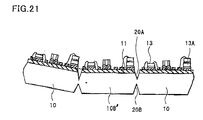
- Fig. 21 is a sectional view showing one illustrative method of partitioning the substrate. In this illustrative method, the metal substrate 10B' is bent to partition it into individual circuit substrates 10.
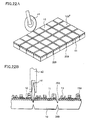
- Fig. 22(A) is a perspective view showing another illustrative method of partitioning the substrate into individual circuit substrates 10 using a circular cutter 41.
- Fig. 22(B) is a sectional view of Fig. 22(A).
- the metal substrate 10B' is preferably bent at a location where a first groove 20A and a second groove 20B have been formed to effect partitioning. Since a location where a first groove 20A and a second groove 20B have been formed is connected only by a thickness part where a groove 20 is not formed, by bending at this location, separation of this connected part can be readily performed.
- the method is carried out in a manner to avoid damaging the electrical circuit formed on the top surface of metal substrate 10B'.
- the partial bending of metal substrate 10B' is preferably performed from the rear surface to avoid damaging the electrical circuit.
- the substrate can be bent downwardly (e.g., opposite to that shown in Fig. 21) to effect separation.
- circular cutter 41 preferably force-cuts the metal substrate 10B' along dicing lines D3. In this manner, the metal substrate 10B' can be readily partitioned into individual circuit substrates 10.
- the circular cutter 41 preferably force-cuts the part of the thickness part of metal substrate 10B' between the grooves 20A and 20B corresponding to the central lines of grooves 20.
- the circular cutter 41 preferably has the shape of a circular disk.
- the peripheral edge part is formed into an acute angle.
- the central part of circular cutter 41 is fixed to a supporting part 42 in a manner enabling free rotation of circular cutter 41 (such as, e.g., so as to rotate about a central axis).
- the circular cutter 41 is preferably not driven by a driving force.
- the circular cutter 41 freely rotates such that it rotates as it is moved along a dicing line D3 while a part of circular cutter 41 is pressed against metal substrate 10B' (e.g., due to the contact therebetween).
- a heat sink 13A and/or another circuit element 13 with some height can be positioned at a peripheral part of circuit substrate 10.
- the position of a heat sink 13A may thus be close to a dicing line D3 as shown in Fig. 10.
- the position of a supporting part 42 can be set so that supporting part 42 will not contact the heat sink 13A in such a case.
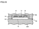
- FIG. 23 is a sectional view, showing the step of sealing circuit substrate 10 in an insulating resin 16 by use of, e.g., a mold die 50.
- circuit substrate 10 is preferably set on a lower mold die 50B.
- Insulating resin 16 can then be injected through a gate 53.
- transfer molding using a thermosetting resin or injection molding using a thermosetting resin can be employed as the method of sealing. Air of an amount corresponding to the amount of the insulating resin 16 that is injected from gate 53 can be ejected from the interior of the cavity to the exterior via an air vent 54.
- inclined parts 10B are preferably provided at side face parts of circuit substrate 10.
- insulating resin 16 is set around the vicinity of inclined part 10B.
- an anchor effect is provided between insulating resin 16 and the inclined part 10B and the joining of insulating resin 16 and circuit substrate 10 can be, thereby, fortified.
- the cross-sectional shape of the part where the rear surface of circuit substrate 10 continues to an inclined part 10B is formed to have an obtuse angle.
- the inclined part is not formed to have a rounded shape (such as, e.g., discussed above with respect to other embodiments). In this manner, entry of the insulating resin 16, which is injected through the gate 53, into parts between lower mold die 50B and the rear surface of circuit substrate 10 can be prevented.
- the circuit substrate 10, which has been sealed in resin in the above-described step can be completed as a product upon being subject to, for example, a lead cutting step, etc.
- partitioning into individual circuit substrates10 is preferably performed after forming a plurality of electrical circuits on the top surface of a large-size metal substrate 10B', this process may be changed in various embodiments.
- an elongated metal substrate, with which two to eight circuit substrates (the number being by way of example only) can be formed in parallel, can be formed prior to mounting electrical circuits on the top surface of the metal substrate.
- the individual circuit substrates can be partitioned.
- the above-described partitioning methods e.g., bending method and/or cutter 41 method
- partitioning methods can be employed as illustrative methods of partitioning the circuit substrates.
- the foregoing embodiments can provide one or more, preferably all, of the following effects.
- flat parts 35B are preferably povided at blade edges 35A of a V-cut saw 35 for forming first grooves 20A and second grooves 20B in metal substrate 10B', the wear of blade edges 35A can be reduced. Additionally, early degradation of the cutting performance of V-cut saw 35 can thus be prevented. Furthermore, even in cases where first grooves 20A are to be formed on the surface of metal substrate 10B' on which resin layer 11 is provided, the formation of cracks in resin layer 11 can be prevented.
- the circuit substrates 10 can be partitioned readily at the locations where the grooves are formed.
- one or both of the following methods of partitioning may be employed: partitioning by bending; or partitioning by circular cutter. And, partitioning can be performed readily with either of these methods.
- the configurations of the grooves 20 can be modified depending on circumstances at hand.
- the grooves 20 can have other cross-sectional configurations, such as, e.g., generally one of a U-shape, a semi-circular shape, a semi-elliptical shape, a rectangular shape, a polygonal shape and/or another desired shape.
- the size (including width and/or depth) of the grooves 20B in the rear of the substrate is preferably larger than the size (including width and/or depth) of the grooves 20A in order to, for example, enable the area for the conductive patterns 12 and the circuit elements 13 to be maximized.
- the apexes of the grooves 20B preferably extend a greater distance into the substrate than the apexes of the grooves 20A. In some embodiments, for example, the apexes of the grooves 20B can extend even past a center plane of the substrate to within a top half of the substrate.
- one or more, preferably both, of the following advantages can be achieved if desired: a) increased mold-lock or anchor effect between the resin and the substrate and b) increased usable area for the conductive patterns and circuit elements.
- any known partitioning means can be employed in various other embodiments.
- a related art punch press partitioning means could be employed or various partitioning means using other cutting means, such as, e.g., utilizing wave sources and/or other means could be employed.
Landscapes
- Engineering & Computer Science (AREA)
- Manufacturing & Machinery (AREA)
- Microelectronics & Electronic Packaging (AREA)
- Insulated Metal Substrates For Printed Circuits (AREA)
- Dicing (AREA)
- Structure Of Printed Boards (AREA)
Abstract
Description
Fig. 15(C) is an enlarged view of the vicinity of a
Claims (28)
- A method of manufacturing a hybrid integrated circuit device, comprising:preparing a metal substrate (10) having an insulating layer (11) over a top surface;forming conductive patterns (12) over said insulating layer (11);forming a lattice of grooves (20) in a rear surface of said metal substrate (10);mounting a hybrid integrated circuit over at least one of said conductive patterns; andseparating individual circuit substrates with a rotatable cutter contacting said metal substrate (10) at locations corresponding to said grooves (20) to cut remaining thicknesses of said metal substrate (10) and said insulating layer (11).
- The method of Claim 1, wherein said rotatable cutter is a circular cutter (41) that rotates without an external drive.
- The method of Claim 1, wherein said rotatable cutter (41) is a rotatable saw.
- The method according to any of Claims 1 to 3, wherein said grooves (20) have a generally V-shaped cross-section.
- The method according to any of Claims 1 to 4, wherein a depth of said grooves (20) is shallower than a thickness of said metal substrate (10).
- The method according to any of Claims 1 to 5, wherein said metal substrate (10) is formed of a material principally comprising aluminum or copper.
- The method according to any of Claims 1 to 6, wherein said metal substrate (10) is an aluminum substrate.
- The method of Claim 7, wherein top and rear surfaces of said aluminum substrate have been subject to alumite treatment.
- The method according to any of Claims 1 to 8, wherein said insulating layer (11) is a resin filled with alumina.
- The method according to any of Claims 1 to 9, wherein in said step of forming the grooves (20), a cutting saw (35), with blade edges (35A) of a shape corresponding to a cross-section of said grooves (20), is rotated at a high speed to form said grooves (20).
- A method of manufacturing a hybrid integrated circuit device, comprising:preparing a metal substrate (10) having an insulating layer (11) over a top surface;forming a plurality of conductive patterns (12) over a top surface of said insulating layer (11);forming lattices of grooves (20A, 20B) in the top and rear surfaces of said metal substrate (10);mounting a hybrid integrated circuit on at least one of said conductive patterns (12); andseparating said metal substrate (10) along said grooves (20A, 20B) into individual circuit substrates.
- The method of Claim 11, wherein said separating includes bending said metal substrate (10) at the locations where said grooves (20A, 20B) were formed to separate said metal substrate (10) into said individual circuit substrates.
- The method of Claim 11, wherein said separating includes separating individual circuit substrates with a rotatable cutter contacting said metal substrate (10) at locations corresponding to said grooves (20A, 20B) to cut remaining thicknesses of said metal substrate (10) and said insulating layer (11).
- The method of Claim 11, wherein said forming lattices of grooves includes using a cutting saw (35), with blade edges (35A) of a shape corresponding to a cross-section of said grooves (20A, 20B), that is rotated at a high speed to form said grooves (20A, 20B).
- The method of Claim 14, wherein the blade edges (35A) of said saw (35) are substantially flat.
- A method of manufacturing an integrated circuit device, comprising:preparing a substrate having an insulating layer (11);forming a plurality of conductive patterns (12) over said insulating layer (11);forming a plurality of grooves (20, 20A, 20B) in at least one of a top or a bottom surface of said substrate; andseparating said metal substrate along said grooves (20) into individual circuit substrates.
- The method of claim 16, wherein said integrated circuit device is a hybrid integrated circuit device and said substrate is a metal substrate (10).
- The method of claim 16 or 17, wherein said grooves (20A, 20B) are formed in both said top and bottom surfaces.
- The method according to any of claims 16 to 18, wherein said grooves (20A, 20B) are generally V-shaped in cross-section and substantially aligned to form thinned regions in said substrate.
- The method of claim 18 or 19, wherein said grooves (20B) in said bottom surface are deeper than said grooves (20A) in said top surface.
- The method according to any of claims 16 to 20, wherein said individual circuit substrates (10) are formed with peripheral sides having inclined parts (10B).
- The method of claim 21, further including sealing said individual circuit substrates (10) in an insulating resin (16).
- The method of claim 21 or 22, further including sealing said individual circuit substrates (10) in an insulating resin (16) by transfer molding.
- The method of claim 23, wherein during said sealing, insulating resin (16) is set around said inclined parts (10B), creating an anchor effect between the insulating resin (16) and the inclined parts (10B).
- The method according to any of claims 21 to 24, wherein said inclined parts (10B) are configured to inhibit entry of resin (16) beneath the substrate (10) during sealing.
- The method according to any of claims 16 to 25, wherein said individual circuit substrates (10) are formed with said conductive patterns (12) very near at least one peripheral end.
- The method according to any of claims 16 to 25, wherein said individual circuit substrates (10) are formed with said conductive patterns (12) within about 2 mm of at least one peripheral end.
- The method according to any of claims 16 to 25, wherein said individual circuit substrates (10) are formed with said conductive patterns (12) within about 1 mm of at least one peripheral end.
Applications Claiming Priority (4)
| Application Number | Priority Date | Filing Date | Title |
|---|---|---|---|
| JP2002121750 | 2002-04-24 | ||
| JP2002121750 | 2002-04-24 | ||
| JP2002253987 | 2002-08-30 | ||
| JP2002253987A JP2004006585A (en) | 2002-04-24 | 2002-08-30 | Manufacturing method of hybrid integrated circuit device |
Publications (2)
| Publication Number | Publication Date |
|---|---|
| EP1359612A2 true EP1359612A2 (en) | 2003-11-05 |
| EP1359612A3 EP1359612A3 (en) | 2006-04-19 |
Family
ID=29218001
Family Applications (1)
| Application Number | Title | Priority Date | Filing Date |
|---|---|---|---|
| EP03009358A Withdrawn EP1359612A3 (en) | 2002-04-24 | 2003-04-24 | Methods of manufacturing a hybrid integrated circuit device |
Country Status (3)
| Country | Link |
|---|---|
| EP (1) | EP1359612A3 (en) |
| JP (1) | JP2004006585A (en) |
| CN (1) | CN100521167C (en) |
Cited By (2)
| Publication number | Priority date | Publication date | Assignee | Title |
|---|---|---|---|---|
| WO2012143353A1 (en) * | 2011-04-20 | 2012-10-26 | Ams Ag | Method for cutting a carrier for electrical components |
| CN109686701A (en) * | 2018-12-27 | 2019-04-26 | 广东晶科电子股份有限公司 | It is a kind of can grain formula separation ceramic substrate and its separation method |
Families Citing this family (8)
| Publication number | Priority date | Publication date | Assignee | Title |
|---|---|---|---|---|
| CN100447981C (en) * | 2006-06-17 | 2008-12-31 | 铜陵三佳科技股份有限公司 | Separation method and mold for surface mount integrated circuit products |
| WO2008078881A1 (en) | 2006-12-26 | 2008-07-03 | Seoul Opto Device Co., Ltd. | Light emitting device |
| JP5108496B2 (en) * | 2007-12-26 | 2012-12-26 | 三洋電機株式会社 | Circuit board and manufacturing method thereof, circuit device and manufacturing method thereof |
| JP2011096865A (en) * | 2009-10-30 | 2011-05-12 | Sharp Corp | Substrate member, module, electric equipment, and manufacturing method of modules |
| CN102036491A (en) * | 2010-12-09 | 2011-04-27 | 北大方正集团有限公司 | Method for molding circuit board and circuit board |
| JP5803998B2 (en) * | 2013-07-23 | 2015-11-04 | 株式会社村田製作所 | Method for manufacturing electronic component and method for manufacturing board-type terminal |
| CN110366318B (en) * | 2019-07-16 | 2021-05-11 | 深圳市星河电路股份有限公司 | Processing technology for reducing distance from V-CUT line to lead |
| CN113851434A (en) * | 2021-09-28 | 2021-12-28 | 广东汇芯半导体有限公司 | Semiconductor circuit and method for manufacturing semiconductor circuit |
Family Cites Families (12)
| Publication number | Priority date | Publication date | Assignee | Title |
|---|---|---|---|---|
| JPH01100995A (en) * | 1987-10-14 | 1989-04-19 | Denki Kagaku Kogyo Kk | Mass production of metal base circuit board |
| JPH01289188A (en) * | 1988-05-16 | 1989-11-21 | Sanyo Electric Co Ltd | Manufacture of low heat-resistance circuit board |
| JPH02237094A (en) * | 1989-03-09 | 1990-09-19 | Sanyo Electric Co Ltd | Manufacture of hybrid integrated circuit |
| JPH06103790B2 (en) * | 1989-06-16 | 1994-12-14 | 富士電機株式会社 | Method for manufacturing aluminum insulating plate |
| DE4035792C1 (en) * | 1990-11-10 | 1992-04-23 | Loehr & Herrmann Gmbh, 7531 Neuhausen, De | Printed circuit board panel de-edging device - has two saw-blades mounted in bearingblockings which can be positionally adjusted |
| JPH0679689A (en) * | 1992-09-03 | 1994-03-22 | Fujitsu Ltd | Printed circuit board divider |
| DE9303098U1 (en) * | 1993-03-03 | 1993-07-08 | Siemens AG, 8000 München | Device for separating interconnected printed circuit boards |
| JPH09162507A (en) * | 1995-12-08 | 1997-06-20 | Nippon Seiki Co Ltd | Metal base printed circuit board |
| TW382736B (en) * | 1996-04-18 | 2000-02-21 | Eastern Kk | Circuit board for a semiconductor device and method of making the same |
| US5834084A (en) * | 1996-06-25 | 1998-11-10 | Seagate Technology, Inc. | Disc drive flex assembly having a low particulating circuit board |
| JPH1022630A (en) * | 1996-06-28 | 1998-01-23 | Nippon Seiki Co Ltd | Method of dividing metal-based printed circuit board |
| US6259157B1 (en) * | 1998-03-11 | 2001-07-10 | Sanyo Electric Co., Ltd. | Hybrid integrated circuit device, and method of manufacturing thereof |
-
2002
- 2002-08-30 JP JP2002253987A patent/JP2004006585A/en active Pending
-
2003
- 2003-04-24 EP EP03009358A patent/EP1359612A3/en not_active Withdrawn
- 2003-04-24 CN CN03123268.XA patent/CN100521167C/en not_active Expired - Fee Related
Cited By (4)
| Publication number | Priority date | Publication date | Assignee | Title |
|---|---|---|---|---|
| WO2012143353A1 (en) * | 2011-04-20 | 2012-10-26 | Ams Ag | Method for cutting a carrier for electrical components |
| US9961777B2 (en) | 2011-04-20 | 2018-05-01 | Ams Ag | Method for cutting a carrier for electrical components |
| CN109686701A (en) * | 2018-12-27 | 2019-04-26 | 广东晶科电子股份有限公司 | It is a kind of can grain formula separation ceramic substrate and its separation method |
| CN109686701B (en) * | 2018-12-27 | 2024-05-10 | 广东晶科电子股份有限公司 | Particle-separable ceramic substrate and separation method thereof |
Also Published As
| Publication number | Publication date |
|---|---|
| CN1453857A (en) | 2003-11-05 |
| CN100521167C (en) | 2009-07-29 |
| EP1359612A3 (en) | 2006-04-19 |
| JP2004006585A (en) | 2004-01-08 |
Similar Documents
| Publication | Publication Date | Title |
|---|---|---|
| US7008825B1 (en) | Leadframe strip having enhanced testability | |
| US20070226996A1 (en) | Hybrid integrated circuit device and method of manufacturing the same | |
| US6956252B2 (en) | Hybrid integrated circuit device | |
| CN103035606B (en) | Based on the flash memory cards of lead frame | |
| US7250352B2 (en) | Methods for manufacturing a hybrid integrated circuit device | |
| CN113140523A (en) | Lead frame, package with die-cut leads and sawn sides, and corresponding methods | |
| JP4488733B2 (en) | A method for manufacturing a circuit board and a method for manufacturing a hybrid integrated circuit device. | |
| US6571595B2 (en) | Method of forming a package for electronic parts | |
| CN100521167C (en) | Method for manufacturing hybrid integrated circuit device | |
| USRE43818E1 (en) | Fabrication of an integrated circuit package | |
| US20240105537A1 (en) | Mold, lead frame, method, and electronic device with exposed die pad packaging | |
| US20050161781A1 (en) | Hybrid integrated circuit device and manufacturing method thereof | |
| JP4606447B2 (en) | A method for manufacturing a metal substrate of an intermediate plate. | |
| JP4039881B2 (en) | Method for manufacturing hybrid integrated circuit device | |
| US5452635A (en) | Apparatus for integrated circuit lead-frame punching | |
| JP2005285909A (en) | Method for manufacturing hybrid integrated circuit device | |
| US7211879B1 (en) | Semiconductor package with chamfered corners and method of manufacturing the same | |
| JP4850216B2 (en) | Method for manufacturing hybrid integrated circuit device | |
| JP2005123606A (en) | Hybrid integrated circuit device and manufacturing method thereof | |
| EP4451327A1 (en) | Method of manufacturing semiconductor devices, corresponding substrate and semiconductor device | |
| JP2009158828A (en) | Lead frame sheet bridge cutting method | |
| JP2004087702A (en) | Apparatus and method for manufacturing semiconductor device |
Legal Events
| Date | Code | Title | Description |
|---|---|---|---|
| PUAI | Public reference made under article 153(3) epc to a published international application that has entered the european phase |
Free format text: ORIGINAL CODE: 0009012 |
|
| AK | Designated contracting states |
Kind code of ref document: A2 Designated state(s): AT BE BG CH CY CZ DE DK EE ES FI FR GB GR HU IE IT LI LU MC NL PT RO SE SI SK TR |
|
| AX | Request for extension of the european patent |
Extension state: AL LT LV MK |
|
| PUAL | Search report despatched |
Free format text: ORIGINAL CODE: 0009013 |
|
| AK | Designated contracting states |
Kind code of ref document: A3 Designated state(s): AT BE BG CH CY CZ DE DK EE ES FI FR GB GR HU IE IT LI LU MC NL PT RO SE SI SK TR |
|
| AX | Request for extension of the european patent |
Extension state: AL LT LV MK |
|
| RIC1 | Information provided on ipc code assigned before grant |
Ipc: H01L 21/304 20060101ALI20060227BHEP Ipc: H05K 3/44 20060101ALI20060227BHEP Ipc: H05K 3/00 20060101AFI20060227BHEP |
|
| 17P | Request for examination filed |
Effective date: 20061017 |
|
| AKX | Designation fees paid |
Designated state(s): DE FR IT NL |
|
| 17Q | First examination report despatched |
Effective date: 20101006 |
|
| STAA | Information on the status of an ep patent application or granted ep patent |
Free format text: STATUS: THE APPLICATION HAS BEEN WITHDRAWN |
|
| 18W | Application withdrawn |
Effective date: 20130718 |