EP1355175A1 - Resonant coupling of optical signals for out-of-plane transmission - Google Patents
Resonant coupling of optical signals for out-of-plane transmission Download PDFInfo
- Publication number
- EP1355175A1 EP1355175A1 EP02023301A EP02023301A EP1355175A1 EP 1355175 A1 EP1355175 A1 EP 1355175A1 EP 02023301 A EP02023301 A EP 02023301A EP 02023301 A EP02023301 A EP 02023301A EP 1355175 A1 EP1355175 A1 EP 1355175A1
- Authority
- EP
- European Patent Office
- Prior art keywords
- optical
- resonant
- signal
- resonant system
- optically resonant
- Prior art date
- Legal status (The legal status is an assumption and is not a legal conclusion. Google has not performed a legal analysis and makes no representation as to the accuracy of the status listed.)
- Withdrawn
Links
- 230000003287 optical effect Effects 0.000 title claims abstract description 158
- 230000008878 coupling Effects 0.000 title claims description 21
- 238000010168 coupling process Methods 0.000 title claims description 21
- 238000005859 coupling reaction Methods 0.000 title claims description 21
- 230000005540 biological transmission Effects 0.000 title description 3
- 239000000758 substrate Substances 0.000 claims description 48
- 238000000034 method Methods 0.000 claims description 38
- 230000005855 radiation Effects 0.000 claims description 32
- 239000000463 material Substances 0.000 claims description 18
- 239000013307 optical fiber Substances 0.000 claims description 13
- 230000005684 electric field Effects 0.000 claims description 8
- 230000001902 propagating effect Effects 0.000 claims description 7
- 230000001747 exhibiting effect Effects 0.000 claims description 5
- 230000004044 response Effects 0.000 claims description 2
- 238000013461 design Methods 0.000 description 12
- 238000010586 diagram Methods 0.000 description 12
- 238000004519 manufacturing process Methods 0.000 description 9
- 230000010363 phase shift Effects 0.000 description 9
- VYPSYNLAJGMNEJ-UHFFFAOYSA-N Silicium dioxide Chemical compound O=[Si]=O VYPSYNLAJGMNEJ-UHFFFAOYSA-N 0.000 description 6
- 230000008569 process Effects 0.000 description 6
- 238000000926 separation method Methods 0.000 description 6
- 230000008901 benefit Effects 0.000 description 5
- 239000003989 dielectric material Substances 0.000 description 5
- 230000014509 gene expression Effects 0.000 description 5
- 239000011159 matrix material Substances 0.000 description 4
- 238000012546 transfer Methods 0.000 description 4
- 238000004364 calculation method Methods 0.000 description 3
- 230000001427 coherent effect Effects 0.000 description 3
- 230000007246 mechanism Effects 0.000 description 3
- 230000004048 modification Effects 0.000 description 3
- 238000012986 modification Methods 0.000 description 3
- 235000012239 silicon dioxide Nutrition 0.000 description 3
- 239000000377 silicon dioxide Substances 0.000 description 3
- XUIMIQQOPSSXEZ-UHFFFAOYSA-N Silicon Chemical compound [Si] XUIMIQQOPSSXEZ-UHFFFAOYSA-N 0.000 description 2
- 238000013459 approach Methods 0.000 description 2
- 230000002238 attenuated effect Effects 0.000 description 2
- 238000006073 displacement reaction Methods 0.000 description 2
- 230000000694 effects Effects 0.000 description 2
- 238000005530 etching Methods 0.000 description 2
- 230000036961 partial effect Effects 0.000 description 2
- 238000004904 shortening Methods 0.000 description 2
- 229910052710 silicon Inorganic materials 0.000 description 2
- 239000010703 silicon Substances 0.000 description 2
- 230000036962 time dependent Effects 0.000 description 2
- 238000004458 analytical method Methods 0.000 description 1
- 238000004891 communication Methods 0.000 description 1
- 239000002131 composite material Substances 0.000 description 1
- 238000012937 correction Methods 0.000 description 1
- 230000003247 decreasing effect Effects 0.000 description 1
- 230000004069 differentiation Effects 0.000 description 1
- 238000009826 distribution Methods 0.000 description 1
- 230000005672 electromagnetic field Effects 0.000 description 1
- 230000007274 generation of a signal involved in cell-cell signaling Effects 0.000 description 1
- 230000001939 inductive effect Effects 0.000 description 1
- 230000010354 integration Effects 0.000 description 1
- 230000000670 limiting effect Effects 0.000 description 1
- 230000003094 perturbing effect Effects 0.000 description 1
- 238000000206 photolithography Methods 0.000 description 1
- 238000012545 processing Methods 0.000 description 1
- 230000000191 radiation effect Effects 0.000 description 1
- 238000002310 reflectometry Methods 0.000 description 1
Images


Classifications
-
- G—PHYSICS
- G02—OPTICS
- G02B—OPTICAL ELEMENTS, SYSTEMS OR APPARATUS
- G02B6/00—Light guides; Structural details of arrangements comprising light guides and other optical elements, e.g. couplings
- G02B6/24—Coupling light guides
- G02B6/26—Optical coupling means
- G02B6/34—Optical coupling means utilising prism or grating
-
- G—PHYSICS
- G02—OPTICS
- G02B—OPTICAL ELEMENTS, SYSTEMS OR APPARATUS
- G02B6/00—Light guides; Structural details of arrangements comprising light guides and other optical elements, e.g. couplings
- G02B6/10—Light guides; Structural details of arrangements comprising light guides and other optical elements, e.g. couplings of the optical waveguide type
- G02B6/12—Light guides; Structural details of arrangements comprising light guides and other optical elements, e.g. couplings of the optical waveguide type of the integrated circuit kind
- G02B6/12002—Three-dimensional structures
-
- G—PHYSICS
- G02—OPTICS
- G02B—OPTICAL ELEMENTS, SYSTEMS OR APPARATUS
- G02B6/00—Light guides; Structural details of arrangements comprising light guides and other optical elements, e.g. couplings
- G02B6/10—Light guides; Structural details of arrangements comprising light guides and other optical elements, e.g. couplings of the optical waveguide type
- G02B6/12—Light guides; Structural details of arrangements comprising light guides and other optical elements, e.g. couplings of the optical waveguide type of the integrated circuit kind
- G02B6/12004—Combinations of two or more optical elements
-
- G—PHYSICS
- G02—OPTICS
- G02B—OPTICAL ELEMENTS, SYSTEMS OR APPARATUS
- G02B6/00—Light guides; Structural details of arrangements comprising light guides and other optical elements, e.g. couplings
- G02B6/10—Light guides; Structural details of arrangements comprising light guides and other optical elements, e.g. couplings of the optical waveguide type
- G02B6/12—Light guides; Structural details of arrangements comprising light guides and other optical elements, e.g. couplings of the optical waveguide type of the integrated circuit kind
- G02B6/12007—Light guides; Structural details of arrangements comprising light guides and other optical elements, e.g. couplings of the optical waveguide type of the integrated circuit kind forming wavelength selective elements, e.g. multiplexer, demultiplexer
-
- G—PHYSICS
- G02—OPTICS
- G02B—OPTICAL ELEMENTS, SYSTEMS OR APPARATUS
- G02B6/00—Light guides; Structural details of arrangements comprising light guides and other optical elements, e.g. couplings
- G02B6/24—Coupling light guides
- G02B6/26—Optical coupling means
- G02B6/28—Optical coupling means having data bus means, i.e. plural waveguides interconnected and providing an inherently bidirectional system by mixing and splitting signals
- G02B6/2804—Optical coupling means having data bus means, i.e. plural waveguides interconnected and providing an inherently bidirectional system by mixing and splitting signals forming multipart couplers without wavelength selective elements, e.g. "T" couplers, star couplers
- G02B6/2852—Optical coupling means having data bus means, i.e. plural waveguides interconnected and providing an inherently bidirectional system by mixing and splitting signals forming multipart couplers without wavelength selective elements, e.g. "T" couplers, star couplers using tapping light guides arranged sidewardly, e.g. in a non-parallel relationship with respect to the bus light guides (light extraction or launching through cladding, with or without surface discontinuities, bent structures)
-
- H—ELECTRICITY
- H01—ELECTRIC ELEMENTS
- H01S—DEVICES USING THE PROCESS OF LIGHT AMPLIFICATION BY STIMULATED EMISSION OF RADIATION [LASER] TO AMPLIFY OR GENERATE LIGHT; DEVICES USING STIMULATED EMISSION OF ELECTROMAGNETIC RADIATION IN WAVE RANGES OTHER THAN OPTICAL
- H01S5/00—Semiconductor lasers
- H01S5/10—Construction or shape of the optical resonator, e.g. extended or external cavity, coupled cavities, bent-guide, varying width, thickness or composition of the active region
- H01S5/18—Surface-emitting [SE] lasers, e.g. having both horizontal and vertical cavities
- H01S5/185—Surface-emitting [SE] lasers, e.g. having both horizontal and vertical cavities having only horizontal cavities, e.g. horizontal cavity surface-emitting lasers [HCSEL]
- H01S5/187—Surface-emitting [SE] lasers, e.g. having both horizontal and vertical cavities having only horizontal cavities, e.g. horizontal cavity surface-emitting lasers [HCSEL] using Bragg reflection
-
- G—PHYSICS
- G02—OPTICS
- G02B—OPTICAL ELEMENTS, SYSTEMS OR APPARATUS
- G02B6/00—Light guides; Structural details of arrangements comprising light guides and other optical elements, e.g. couplings
- G02B6/24—Coupling light guides
- G02B6/42—Coupling light guides with opto-electronic elements
- G02B6/4201—Packages, e.g. shape, construction, internal or external details
- G02B6/4204—Packages, e.g. shape, construction, internal or external details the coupling comprising intermediate optical elements, e.g. lenses, holograms
- G02B6/4214—Packages, e.g. shape, construction, internal or external details the coupling comprising intermediate optical elements, e.g. lenses, holograms the intermediate optical element having redirecting reflective means, e.g. mirrors, prisms for deflecting the radiation from horizontal to down- or upward direction toward a device
Definitions
- the present invention is generally related to optics and, more particularly, to systems and methods for redirecting optical signals.
- Integrated optical devices are rapidly achieving signal generation and processing functionality previously restricted to the purely electronic domain.
- These . devices which are typically planar, normally include a planar waveguide supported by a substrate, the planar waveguide confining light in the substrate.
- These problems are difficult to solve efficiently, and in the past, engineers have used various solutions with varying degrees of success. These solutions can generally be divided into two categories: end-fire emission and controlled surface emission.
- End-fire emission is a simplistic way to extract light from a planar waveguide.
- a waveguide carries the light to the edge or "end" of a substrate. The light then radiates out of the edge of the waveguide.
- the end-fire emission solution generally only works if a clean edge of the substrate is available, which is often not the case. Further, as electronics are made smaller and smaller, optics used to focus and/or match the light to or from an optical fiber take up too much space.
- Controlled surface emission is widely seen as the solution to at least some of the problems associated with end-fire emission.
- prism-based involves placing a prism on top of a waveguide and refracting emissions from the waveguide.
- Using the prism-based method is impractical. This is because the prism-based technique involves placing a bulk optical component over the waveguide with relative precision.
- the grating-based technique involves etching a grating, i.e. multiple notches, into the surface of a waveguide. The grating causes some of the light propagating in the waveguide to leak out of the substrate surface.
- the grating produces diffuse light that is diffracted into a multitude of directions. Further, these controlled surface emission techniques tend to suffer from the standpoint that both of them are distributed in nature, which can cause spatial distortion and expansion of an extracted mode of the light. As such, these outputs can be difficult to match to an optical fiber.
- an optically resonant system of the invention includes a first structure residing substantially in a plane.
- the first structure reflects optical radiation in a first direction substantially orthogonal to the plane.
- the optically resonant system also includes a second structure overlapping, and optically communicating with the first structure.
- the second structure reflects optical radiation in a direction substantially parallel to the plane.
- the first and second structures operate to capture a at least a portion of a first optical signal propagating substantially parallel to the plane by exciting a resonant signal in a resonant cavity through resonant characteristics of the first and second structures.
- the first and second structures further operate to emit the resonant signal propagating in a second direction substantially orthogonal to the plane.
- the present invention is particularly useful as an integrated optical device residing in an optical substrate.
- an integrated optical device can be used to couple an optical wave travelling in the substrate to an optical fiber for transport or to another integrated optical device located on another substrate, for example.
- an optically resonant system includes a resonant cavity.
- the resonant cavity of the optically resonant system receives a first optical signal exhibiting a directional component.
- the resonant cavity includes a resonant characteristic, resonating in response to the first optical signal to excite and emit a resonant signal.
- the emitted resonant signal has a directional component different than the directional component of the first optical signal.
- a method for making an optically resonant system includes: overlapping a first structure residing substantially in a plane with a second structure operable to optically communicate with the first structure, and defining a resonant optical cavity to capture optical energy from a first optical signal, the resonant optical cavity being at least partly surrounded by the first and second structures.
- a method for redirecting optical radiation includes: receiving a first optical signal exhibiting a directional component and including at least one wavelength; exciting a resonant signal with the first optical signal at said at least one wavelength; and emitting the resonant signal, the resonant signal exhibiting a directional component different than the directional component of the first optical signal.
- FIG. 1 shown is a block diagram illustrating an embodiment of the present invention.
- an optical input signal 100 is provided to an optically resonant system 101.
- the optically resonant system 101 captures energy of the optical input signal 100 through resonant characteristics of the optically resonant system 101.
- the optically resonant system 101 then emits an optical output signal 102.
- the optical output signal could be emitted orthogonal to the optical input signal 100.
- the optical input signal 100 in different embodiments could be travelling in a number of different media, including an optical fiber waveguide, a dielectric waveguide, free space, etc.
- the optical output signal 102 that is emitted may be attenuated, but typically retains any "information content" that may have been encoded on the optical input signal 100.
- the optical output signal 102 in one embodiment, among others, has an axially symmetric radiation pattern that is ideal for coupling the output signal into an optical fiber, or another integrated optical device.
- an optical input signal 200 travels into a substrate region 201, near an optically resonant system 202.
- the optically resonant system 202 captures a portion of the signal and generates an optical output signal 204.
- the optical output signal could be emitted in a direction orthogonal to the optical input signal 200.
- the optically resonant system works by capturing the evanescent fields 203 associated with the optical input signal 200 in the optically resonant system 202.
- Evanescent fields are created when a signal is propagating in a waveguide.
- the optical input signal due to its electromagnetic nature, inherently develops an evanescent field surrounding the waveguide.
- the evanescent field 203 created proximate to the optically resonant system by the optical input signal 200 resonates with at least one mode of the optically resonant system 202, causing optical energy to be transferred into the optically resonant system 202.
- the optically resonant system 202 then preferentially emits the optical energy in a desired direction to producing the optical output signal 204.
- the optical output signal 204 created by the optically resonant system 202 may be attenuated, but typically retains any "information content" that may have been encoded on the input signal 200.
- the output signal 204 in one embodiment, among others, has an axially symmetric radiation pattern that is ideal for coupling the optical output signal into an optical fiber, or into another integrated optical device.
- the optically resonant system receives an optical signal.
- resonant characteristics are used to generate a second optical signal.
- the second signal is emitted.
- the optically resonant system typically receives an optical signal through a waveguide.
- This waveguide can terminate in the optically resonant system, or alternatively, the waveguide can continue through the optically resonant system.
- the evanescent fields which extend outside the waveguide allow coupling of the optical signal to the optically resonant system.
- An asymmetrical containment profile of the optically resonant system can allow the optically resonant system to preferentially emit the second optical signal.
- the emitted optical signal can then be coupled to another integrated optical device or simply an optical fiber to transport the emitted optical signal to another location.
- the present embodiment of the optically resonant system shown in free space, includes a dielectric structure 400.
- the dielectric structure 400 involves a first structure of dielectric parallel plates 401a-f, and a second structure of dielectric concentric cylinders 402a-c.
- the first structure of the optically resonant system overlaps, and is in optical communication with, the second structure of the optically resonant system to capture at least a portion of an optical input signal.
- the first and second structures then operate to emit an output signal.
- the optical output signal can be emitted in a direction orthogonal to the optical input signal.
- the optically resonant system 400 includes a plurality of plates 401a-f and a plurality of cylinders 402a-c which intersect with each other to form a central cavity 500 with resonant characteristics.
- Each of the plates 401a-f resides in the x-y plane, and partially reflects optical energy along the z-axis, orthogonal to the x-y plane.
- Each of the cylinders 402a-c partially reflects light in the radial direction, parallel to the x-y plane.
- the plates 401a-f and cylinders 402a-c are formed from the same dielectric material or similar dielectric materials.
- one such dielectric material that could be used is silicon dioxide.
- a surrounding material, or optical substrate 501 is typically formed from a dielectric material having a lower dielectric constant than the material which forms the plates 401a-f and cylinders 402a-c.
- a typical dielectric constant for the plates and cylinders could be about 11, and a typical dielectric constant for the surrounding material could be about 2.
- many different pairs of dielectric constants can operate to form the optically resonant system and the invention is not limited to merely the dielectric constants disclosed.
- the plates 401a-f and cylinders 402a-c operate to capture certain wavelengths of light. These wavelengths of light are captured according to the dimensions and materials of the optically resonant system 400, as will be fully described in detail below.
- the optically resonant system 400 shown formed in an optical substrate 501, can generally be described as an out-of-plane coupler used to redirect an optical signal, and more specifically as a three dimensional distributed Bragg reflector.
- the optically resonant system 400 captures light through the resonant characteristics of the system.
- the characteristics of the optically resonant system are defined according to the dimensions of the system and refraction properties of the dielectric materials comprising the system.
- the optically resonant system 400 has a symmetrical radiation pattern, radiating captured optical energy substantially in all directions.
- This radiation pattern can be altered by modifying structure of the optically resonant system 400.
- This modification of the optically resonant structure can be achieved by modifying the fabrication of the optically resonant system 400 or by modifying the optically resonant system 400 after fabrication.
- First will be discussed an asymmetric structure which can radiate, preferentially, in one direction, then will be discussed a symmetric structure which can radiate, preferentially, in two directions.
- a fabricator can alter the radiation pattern of the optically resonant system 400 by forming an asymmetric structure that radiates, preferentially, optical energy through the asymmetry of the optically resonant system 400.
- Such an asymmetrical structure could be accomplished by building the optically resonant system 400 with an asymmetrical structure.
- at least one of the plates 401a-f or cylinders 402a-c, or a portion thereof could be left out to cause the optically resonant system 400 to radiate, preferentially.
- the optically resonant system 400 of the invention can also be used as an out-of-plane coupler such as by structuring the optically resonant system as an axially symmetric resonant structure and embedding the optically resonant system 400 in an integrated optical device, as illustrated in FIG. 5.
- Inducing the optically resonant system 400 formed in an optical substrate to emit radiation out of the substrate surface is achieved by using fewer pairs of plates relative to the number of cylinders in the optically resonant system 400.
- the optically resonant system has a relatively high Q-factor, and couples to a plurality of evanescent fields extending outside the core of a proximal planar waveguide.
- the optically resonant system 400 is further structured to emit optical radiation in a direction orthogonal to the proximal planar waveguide.
- the resonant coupling between the proximal planar waveguide and the central cavity can be matched by appropriate design and relative placement of the two components, as will be described in detail below.
- the number of periods of reflectors (plates 401a-f and cylinders 402a-c) of the optically resonant system, in all dimensions, is chosen to achieve adequate coupling between the optically resonant system 400 and the proximal planar waveguide.
- the number of periods of reflectors of the optically resonant system can be further chosen to cause radiation out of the plane to be the dominant energy loss mechanism for the optically resonant system 400.
- Using a structure in which the containment characteristics are asymmetrical for extracting energy from a planar waveguide has the advantage of emitting an out-of-plane signal from a single resonant mode, with an axially symmetric radiation pattern reflective of the radial symmetry of the resonant mode.
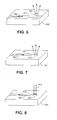
- FIG. 6 shown is a schematic diagram illustrating a first functionality of the optically resonant system of FIG. 5.
- a physical process useful in order to understand the basic operation of the optically resonant system 400 is the mechanism by which an optical input signal 600 is coupled into the optically resonant system 400 from a nearby waveguide 601 in an optical substrate 602.
- Typical geometries are shown in FIGS. 6 and 7, where the waveguide modes can be either travelling or standing waves.
- FIG. 6 illustrates an embodiment in which the optical input signal 600 is coupled into the optically resonant system 400 through evanescent fields surrounding the waveguide 601. These evanescent fields excite the modes of the resonant cavity of the optically resonant system 400 and transfer optical energy within the optically resonant system 400 from the waveguide 601. The optically resonant system 400 then radiates the optical energy from the surface of the substrate to form a second signal.
- FIG. 7 illustrates an embodiment whereby the optical input signal 600 forms a standing wave that couples energy to the optically resonant system 400 via the evanescent fields surrounding waveguide 700 in substrate 701.
- the optically resonant system 400 through the resonant properties of the system captures optical energy of the optical input signal 600 and uses the optical energy to create an optical output signal.
- the optically resonant system 400 then emits the second optical signal through the substrate surface. It is assumed for each of these geometries that the waveguide modes are spatially normalizable, and have the bulk of their energy confined to the core of the waveguides 601 and 700, with calculable evanescent fields outside the core.
- the system can also be used to couple energy into a waveguide of an integrated optical device from optical sources above the substrate surface.
- an optical input signal 800 is directed into the optically resonant system 400.
- the optically resonant system 400 then captures energy from the optical input signal and generates an optical output signal 801 and directs the optical output signal 801 into the waveguide 802 formed in the substrate 803.
- the optically resonant system in this embodiment could have an asymmetric containment characteristic that radiates substantially into the waveguide 802. As one skilled in the art will recognize this can be accomplished by forming the optically resonant system 400 with an asymmetrical structure in the radial direction.
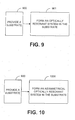
- the first step 900 is to provide a substrate.
- the next step 901 is to form a resonant cavity.
- Step 901 has been compressed in this process, but typically includes a series of fill and backfill steps marked by intermediate photolithography steps, as known to those skilled in the art.
- the user can also fabricate a waveguide during step 901 of the present method for making the optically resonant system 400.
- etch and backfill steps typically could include using a layer by layer approach to fabricating the optically resonant system.
- a fabricator could etch at least one ring into an optical substrate formed from a first material, such as silicon dioxide.
- the fabricator could fill the ring(s) and deposit a plate with a second material, such as silicon. Then, the fabricator could deposit the first material over the plate, and repeat this process until a desired number of cylinders and plates have been fabricated.
- the fabricator could first deposit a layer of the second material over the substrate. The fabricator could then etch the second material layer to form at least one ring over the substrate. Next, the fabricator could deposit a layer of the substrate first material to fill in the gaps in the ring layer. The fabricator could then deposit a plate layer of the second material, etch the plate, and fill in the gaps in the plate layer. Then the fabricator could repeat each these steps until a desired number of cylinders and plates have been formed.
- These fabrication methods are merely examples of fabrication methods that may be used, however, one skilled in the art will recognize that there exist numerous different methods to fabricate a given structure.
- the number of plates and cylinders defines a containment strength of the optically resonant system.
- the containment strength defines the ability of the optically resonant system 400 to keep a resonant signal contained within the optically resonant system after capturing the resonant signal.
- This containment strength can be increased or decreased according to the number of plates or cylinders that are included in the optically resonant system, as will be discussed below.
- the number of plates or cylinders can be adjusted to compensate for specific design considerations of each application.
- the fabricator can etch a completed optically resonant system 400 in order to adjust the optical power radiated from the resonant cavity.
- Step 1000 allows the user to form an optically resonant system having an asymmetrical structure. Instead of forming a completely symmetrical structure, at least a portion of one or more of the outer plates or cylinders are left out during fabrication. Thus, an asymmetric optically resonant system is formed which will radiate, preferentially, toward the asymmetry in the structure.
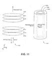
- the first structure 1100 includes a plurality of parallel plates 401a-f. These plates 401a-f lie in the x-y plane, and partially reflect optical energy in the direction of the z-axis, orthogonal to the x-y plane. Thus the first structure can be called a one-dimensional (1-D) reflector.
- the second structure 1101, includes a plurality of concentric cylinders 402a-c. The cylinders 402a-c partially reflect optical radiation radially from the cylinders 402a-c. Thus the second structure can be called a two-dimensional (2-D) reflector.
- TE Transverse Electric
- Equation (1) is the constant value of the dielectric constant of the first and second structures 1100, 1101.
- Equation (2) is the last term in Equation (2) describing the dielectric constant of the combined first and second structures.
- This term proportional to f 1 ( p ) f 2 ( z ), is required so that the dielectric constant value is not double-counted in the regions of intersection of the plates and cylinders 401a-f, 402a-c.
- Equation (1) is not separable between the p and z dimensions, then the set of plates 401a-f comprising the 1-D reflectors and the set of cylinders 402a-c comprising the 2-D reflectors do not act independently. Thus, the 1-D and 2-D reflectors could not be simply combined to create a 3-D confining structure.
- This mode choice is the TE 0 resonant mode, which has electric field nulls at the inner surfaces of all plates and cylinders 401a-f, 402a-c, when following coherent design rules for the optically resonant system 400. Separability is restored when the electric field values experience a "double-null" (from the ⁇ and z dimensions) at non-separable regions of intersection between the plates and cylinders 401 a-f, 402a-c of the optically resonant system 400. Thus, the non-separable term can be deleted from the equation. The numerical error associated with this approximation can be shown to be extremely small using perturbative techniques.
- Equation (4) calculates for an optically resonant system in free space, as in FIG. 4.
- Equation (5) becomes completely separable, and B z can be rewritten as B z ( ⁇ , z ) ⁇ R ( ⁇ ) Z ( z ).
- the partial differential equation can be written as two ordinary differential equations where ⁇ 2 ( ⁇ 1 ) is the higher (lower) dielectric constant of the structure 400, and ⁇ is the separation constant.
- the separation constant is a mathematical term for a constant that must be included in both ordinary differential equations in order to for the single partial differential equation to be separable.
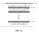
- Equation 13 yielding 2x2 matrix equations connecting the coefficients in each separate region Restricting to a lowest resonant (spatially even) solution, and imposing the fact that the E-field is zero at an upper surface of the optically resonant system, a transcendental equation is derived for the separation constant, ⁇ where H is the height of the optically resonant system 400.
- the separation constant, ⁇ is determined from Equations (12) and (17) numerically, and subsequently all of the coefficients A i and B i are determined by matrix concatenation.
- the field in the central cavity 500 can be connected to those in an outer region using the 2x2 transfer matrices, determined from matching fields at the interfaces,
- D 1 is zero, since the Y-functions are singular for a zero argument. Therefore, the equation for the phase shift is The full solution, and all coefficients, are calculated by matrix concatenation.
- a plot of Q versus ⁇ displays a number of broad peaks where energy is preferentially stored in the structure, i.e. weak resonances, and a single peak of very high Q corresponding to the TE 0 mode where all plates and cylinders 401a-f, 402a-c are acting coherently to efficiently trap light radiation.
- FIG. 15 shows a plot for a typical optically resonant system including four cylinder regions, four plate pair regions, and dielectric constants of 11.56 and 2.25 for the optically resonant system and background regions, respectively. Note the extremely high Q of the TE 0 mode, indicating the efficiency of the optically resonant system created using design rules discussed herein.
- the analysis technique used to determine the coupling of the waveguide structure 601 (FIG. 6) and the optically resonant system 400 is a version of coupled mode theory.
- the first step is to write down the dynamical equations for the electromagnetic fields as derived from Maxwell's equations where a "dot" above a field denotes a time derivative, ⁇ o is the free-space permittivity, and ⁇ r is the relative permittivity of the ponderable media. Note, as before, that the inhomogeneous terms in the above wave equations are terms that have the sole purpose of ensuring proper boundary conditions between regions of different dielectric constant.
- Equation (27) Plugging the solution ansatz of a Equation (27) into dynamical Equation (23), using the unperturbed field equations, and approximations that
- Equations (28) can be multiplied by one of the unperturbed fields and integrated over all space.
- ⁇ is a small parameter which characterizes the magnitude of the overlap between the evanescent fields and the perturbing structures.
- the solutions to Equations (33) and (35) have the form where The "coupling rate,” ⁇ , is easily calculable from the expressions for the unperturbed fields, optically resonant system 400 and waveguide 601 as previously described. Clearly, the rate of transfer of energy between the waveguide and the optically resonant system increases as the waveguide 601 and optically resonant system 400 are brought closer together, and have larger evanescent field overlaps.
- the optically resonant system 400 structures can be used in any application where it is desired to extract optical energy from a substrate surface.
- Optical energy can be coupled from virtually any integrated optical device to the optically resonant system 400 through evanescent fields, and ultimately directed out of the substrate surface in the form of optical energy.
- These integrated optic structures can range from waveguides to resonant structures, and the coupling to the optically resonant system can be accurately controllable in a calculable way, as shown in the foregoing discussion.
- the optical energy radiated out of the substrate surface can be directed to other devices or detectors via free-space transmission, or efficiently collected by an optical fiber.
- the radiated optical energy is ideally suited for coupling into an optical fiber, since the output beam has a circular symmetry and a beam diameter on the order of the output wavelength.
- multiple optically resonant systems 400 can be fabricated on a single integrated optic device. Due to the wavelength specific nature of these optically resonant systems 400, it is possible to have all of the couplers operating at the same wavelength, or a series of wavelengths. In all of these applications, the fabrication steps involved in producing an optically resonant system 400 are compatible with the standard growth procedures of typical integrated optic devices. The two-material structures can be grown by a process of selective etching and back-filling during the fabrication of the associated integrated optics device.
- the design rules of the present invention will now be discussed.
- the practical design rules of the optically resonant system 400 begin with specification of the desired resonant frequency, co, and the z-height of the resonant optical cavity 500, L , as the only required inputs (assuming the two dielectric constants, ⁇ 1 and ⁇ 2 are given as a constraint of the materials system under consideration).
- the desired frequency is usually set by the requirements of the application
- the resonant optical cavity 500 height can be adjusted to give a desirable aspect ratio for the dimensions of the resonant optical cavity 500.
- Obtaining a desirable aspect ratio typically includes shortening the height of the resonant optical cavity 500 with respect to the radius of the resonant optical cavity 500. This shortening results in more radiation leaking from the resonant optical cavity 500 along the z-axis of the optically resonant system.
- a first design rule is that the plate and cylinder regions 401a-f, 402a-c (FIG. 5) have thicknesses equal to one-quarter of the wavelength of the desired input signal. This maximizes the reflectivities of the plate and cylinder regions, and thus minimize the number of sections needed.
- Additional plate region positions are determined by extending the resonant optical cavity 500 harmonic solution along the z -axis, and placing the inner surfaces of each additional plate region reflector at the sequential field nulls.
- the harmonic solution. phase shift is corrected for an additional phase drop across the plate regions interior to the current position. This correction takes place because each plate causes a slight movement in the location where the next E-field null is expected to occur. Therefore, when placing the second plate pair 401b and 401e, one must account for a slight displacement of the second E-field null by the first plate pair 401c and 401d. In turn, when placing the third plate pair 401a and 401f, one must account for a slight displacement of the third E-field null by the first and second plate pairs 401c and 401d, and 401b and 401e, respectively.
- additional cylinder region positions are determined by extending the resonant optical cavity 500 radial Bessel function solution, and placing the inner surface of each additional cylinder region reflector at the positions of the E-field nulls, again correcting for an additional phase shift induced by the cylinder regions interior to the current position.
- the first cylinder 402a would have an inner radius of 1.140 ⁇ m, and an outer radius of 1.265 ⁇ m.
- the second cylinder 402b would have an inner radius of 1.737 ⁇ m and an outer radius of 1.860 ⁇ m.
- the third cylinder would have an inner radius of 2.329 ⁇ m and an outer radius of 2.452 ⁇ m.
- Each of the plates would have a thickness of .1175 ⁇ m, with .310 ⁇ m spacing between each of the plates, with the exception of the plates bordering the central cavity.
- the plates 401c, 401d bordering the central cavity would have a spacing of .620 ⁇ m between them.
- the resonant optical cavity in one embodiment, among others, could have a height of .620 ⁇ m and a radius of 1.140 ⁇ m, in order to capture an optical signal with a wavelength of 1.55 ⁇ m.
- the optically resonant system 400 is formed asymmetrically by forming the optically resonant system without an even number of plates 401a-e. In this way, the dominant radiation mechanism for the asymmetric optically resonant system 1501 is no longer in the radial direction into the substrate 501, but is out of the plane, as indicated by radiation 1502 in FIG. 15.
- Equations for electric and magnetic fields far from the substrate surface 1500 take the form where r is the distance from the point on the surface to the observation point, k is the free space wave vector, da' is the surface area differential element to be integrated over the surface S, and n and' is the surface normal unit vector.
- Resonator fields on the surface S needed to complete the integrations of Equations (55) and (56) are known from the previous calculations.
- the asymmetric optically resonant system mode solutions are given as products of Bessel and trigonometric functions as shown in Equations (9, 10, and 13-15). This simple solution form allows the integrals of Equations (23) and (24) to be done analytically yielding closed form expressions for the radiated fields.
- a structure including ten cylinder regions and three plate pair regions, with dielectric constants of 11.56 and 2.25 for the optically resonant system 1501 and background regions 501, respectively, is specified using the design rules.
- the computed Q of the-resonator is 1.0 x 10 8 , when no materials losses are taken into account. This computed Q is only due to radiation losses in the radial direction into the substrate 501. A measured Q would, of course, be much lower due to materials losses.
- the optically resonant system 400 is built asymmetrically without the top high-dielectric plate region, radiation out of the substrate is calculated to generate a Q of 2 x 10 6 .
- the resonant mode of the asymmetric optically resonant system 1501 roughly 50-times more energy is likely to escape through the upper surface of the asymmetric optically resonant system 1501 than leak into the substrate 501.
- the optically resonant system 1501 is built asymmetrically without the top two high-dielectric plate regions, radiation out of the substrate is calculated to generate a Q of 5.7 x 10 4 .
- the asymmetrical optically resonant system 1501 radiates very strongly out of the substrate, with roughly 2000-times more energy radiated out of the substrate than into the substrate. From the example, it is clear that the coupling of the asymmetric optically resonant system resonant modes to radiation fields out of the substrate can be adjusted over a very broad range.
- an efficient out-of-plane coupler has been realized using an optically resonant system with a resonant cavity that can be formed in an integrated optic device.
- the optically resonant system can transfer optical energy from a proximal component of the integrated optic device, such as a waveguide, and direct it out of the optically resonant system with calculable coupling efficiency.
- the output of the optically resonant system has the advantage of being axially symmetric, with a beam diameter on the order of the radiation wavelength.
Landscapes
- Physics & Mathematics (AREA)
- General Physics & Mathematics (AREA)
- Optics & Photonics (AREA)
- Engineering & Computer Science (AREA)
- Microelectronics & Electronic Packaging (AREA)
- Condensed Matter Physics & Semiconductors (AREA)
- Electromagnetism (AREA)
- Optical Couplings Of Light Guides (AREA)
- Optical Integrated Circuits (AREA)
Applications Claiming Priority (2)
| Application Number | Priority Date | Filing Date | Title |
|---|---|---|---|
| US123656 | 2002-04-16 | ||
| US10/123,656 US7003185B2 (en) | 2002-04-16 | 2002-04-16 | Resonant coupling of optical signals for out-of-plane transmission |
Publications (1)
| Publication Number | Publication Date |
|---|---|
| EP1355175A1 true EP1355175A1 (en) | 2003-10-22 |
Family
ID=28674669
Family Applications (1)
| Application Number | Title | Priority Date | Filing Date |
|---|---|---|---|
| EP02023301A Withdrawn EP1355175A1 (en) | 2002-04-16 | 2002-10-17 | Resonant coupling of optical signals for out-of-plane transmission |
Country Status (3)
| Country | Link |
|---|---|
| US (1) | US7003185B2 (enExample) |
| EP (1) | EP1355175A1 (enExample) |
| JP (1) | JP2003315577A (enExample) |
Families Citing this family (6)
| Publication number | Priority date | Publication date | Assignee | Title |
|---|---|---|---|---|
| US7027679B1 (en) | 2004-09-23 | 2006-04-11 | Curt Alan Flory | Resonant coupling of optical signals for out-of-plane transmission that includes output beam modification |
| US8369659B2 (en) | 2006-03-22 | 2013-02-05 | The Invention Science Fund I Llc | High-Q resonators assembly |
| US20110190167A1 (en) * | 2006-03-22 | 2011-08-04 | Hillis W Daniel | Electromagnetically responsive element with self resonant bodies |
| US20080112663A1 (en) * | 2006-03-22 | 2008-05-15 | Searete Llc, A Limited Liability Corporation Of The State Of Delaware | Layered electromagnetically responsive assembly |
| US8693894B2 (en) * | 2008-04-28 | 2014-04-08 | Hewlett-Packard Development Company, L.P. | Gain clamped optical device for emitting LED mode light |
| EP3118661A4 (en) * | 2014-03-28 | 2017-03-29 | Huawei Technologies Co., Ltd. | Optical interconnection device, optoelectronic chip system, and optical signal sharing method |
Citations (3)
| Publication number | Priority date | Publication date | Assignee | Title |
|---|---|---|---|---|
| WO2001063336A1 (en) * | 2000-02-23 | 2001-08-30 | Princeton Lightwave Inc. | Absorption matched ring resonator modulator/switch priority |
| EP1176438A1 (en) * | 1999-02-09 | 2002-01-30 | Kanagawa Academy Of Science And Technology | OPTICAL WAVEGUIDE WAVELENGTH FILTER WITH RING RESONATOR AND 1xN OPTICAL WAVEGUIDE WAVELENGTH FILTER |
| GB2366666A (en) * | 2000-09-11 | 2002-03-13 | Toshiba Res Europ Ltd | Optical device |
Family Cites Families (16)
| Publication number | Priority date | Publication date | Assignee | Title |
|---|---|---|---|---|
| US4720160A (en) * | 1981-12-16 | 1988-01-19 | Polaroid Corporation | Optical resonant cavity filters |
| US4592043A (en) * | 1983-07-08 | 1986-05-27 | At&T Bell Laboratories | Wavelength division multiplexing optical communications systems |
| WO1986002171A1 (en) * | 1984-10-01 | 1986-04-10 | Polaroid Corporation | Optical waveguide amplifier and laser |
| US4955028A (en) * | 1988-03-25 | 1990-09-04 | At&T Bell Laboratories | Wavelength tunable composite cavity laser |
| JP2928532B2 (ja) * | 1988-05-06 | 1999-08-03 | 株式会社日立製作所 | 量子干渉光素子 |
| US5022730A (en) * | 1989-12-12 | 1991-06-11 | At&T Bell Laboratories | Wavelength tunable optical filter |
| DE4042532C2 (de) * | 1990-08-22 | 1994-12-15 | Deutsche Forsch Luft Raumfahrt | Hochfrequenzangeregter Hochleistungslaser |
| US5357591A (en) * | 1993-04-06 | 1994-10-18 | Yuan Jiang | Cylindrical-wave controlling, generating and guiding devices |
| US5647036A (en) * | 1994-09-09 | 1997-07-08 | Deacon Research | Projection display with electrically-controlled waveguide routing |
| US5828688A (en) * | 1995-10-26 | 1998-10-27 | The United States Of America As Represented By The Administrator Of The National Aeronautics And Space Administration | Method and apparatus for linewidth reduction in distributed feedback or distributed bragg reflector semiconductor lasers using vertical emission |
| JPH09260598A (ja) * | 1996-03-19 | 1997-10-03 | Fujitsu Ltd | 光半導体記憶装置 |
| US6052495A (en) * | 1997-10-01 | 2000-04-18 | Massachusetts Institute Of Technology | Resonator modulators and wavelength routing switches |
| US6668000B2 (en) * | 1999-07-15 | 2003-12-23 | University Of Maryland, Baltimore County | System and method of optically testing multiple edge-emitting semiconductor lasers residing on a common wafer |
| US6580739B1 (en) * | 1999-09-02 | 2003-06-17 | Agility Communications, Inc. | Integrated opto-electronic wavelength converter assembly |
| IL135806A0 (en) * | 2000-04-24 | 2001-05-20 | Lambda Crossing Ltd | A multi layer integrated optical device and a method of fabrication thereof |
| US6515305B2 (en) * | 2000-09-18 | 2003-02-04 | Regents Of The University Of Minnesota | Vertical cavity surface emitting laser with single mode confinement |
-
2002
- 2002-04-16 US US10/123,656 patent/US7003185B2/en not_active Expired - Fee Related
- 2002-10-17 EP EP02023301A patent/EP1355175A1/en not_active Withdrawn
-
2003
- 2003-04-15 JP JP2003109783A patent/JP2003315577A/ja active Pending
Patent Citations (3)
| Publication number | Priority date | Publication date | Assignee | Title |
|---|---|---|---|---|
| EP1176438A1 (en) * | 1999-02-09 | 2002-01-30 | Kanagawa Academy Of Science And Technology | OPTICAL WAVEGUIDE WAVELENGTH FILTER WITH RING RESONATOR AND 1xN OPTICAL WAVEGUIDE WAVELENGTH FILTER |
| WO2001063336A1 (en) * | 2000-02-23 | 2001-08-30 | Princeton Lightwave Inc. | Absorption matched ring resonator modulator/switch priority |
| GB2366666A (en) * | 2000-09-11 | 2002-03-13 | Toshiba Res Europ Ltd | Optical device |
Also Published As
| Publication number | Publication date |
|---|---|
| US20030194169A1 (en) | 2003-10-16 |
| JP2003315577A (ja) | 2003-11-06 |
| US7003185B2 (en) | 2006-02-21 |
Similar Documents
| Publication | Publication Date | Title |
|---|---|---|
| US7965914B2 (en) | Critically coupled microring resonator and method | |
| Heebner et al. | Optical microresonators: theory, fabrication, and applications | |
| EP2866067A1 (en) | Grating based optical coupler | |
| US7397987B2 (en) | Resonantly enhanced grating coupler | |
| Brunetti et al. | Comprehensive mathematical modelling of ultra-high Q grating-assisted ring resonators | |
| JP2015111255A5 (enExample) | ||
| US7486855B2 (en) | Optical microresonator | |
| Sırmacı et al. | All‐Dielectric Huygens’ Meta‐Waveguides for Resonant Integrated Photonics | |
| D'Mello et al. | Integration of periodic, sub‐wavelength structures in silicon‐on‐insulator photonic device design | |
| US6782169B2 (en) | System for efficient coupling to photonic crystal waveguides | |
| Boriskina et al. | Tuning of elliptic whispering-gallery-mode microdisk waveguide filters | |
| US9291774B1 (en) | Polarization dependent whispering gallery modes in microspheres | |
| EP1355175A1 (en) | Resonant coupling of optical signals for out-of-plane transmission | |
| Lebbe et al. | Shape optimization for the design of passive mid-infrared photonic components | |
| Wongcharoen et al. | Accurate characterization of optical filters with two-dimensional confinement | |
| US9703037B2 (en) | Resonator optimisation | |
| US20080107388A1 (en) | Optical waveguide device | |
| US20240055829A1 (en) | Semiconductor Laser and Design Method Therefor | |
| Sovizi et al. | Simulation and analysis of ultra-small optical microdisk resonators with random edge roughness: Modification of the matrix model | |
| US7224868B2 (en) | Radiation-free optical cavity | |
| Gu et al. | Unconventional modes induced chiral symmetry breaking in optical microcavity | |
| WO2021224240A1 (en) | Polarization selective resonator | |
| CN100529936C (zh) | 包括输出光束改变的离面传输光信号谐振耦合 | |
| Scheuer et al. | Annular Bragg defect mode resonators | |
| Rabelink | Photonic crystal nanocavities on fiber tips: design and characterization |
Legal Events
| Date | Code | Title | Description |
|---|---|---|---|
| PUAI | Public reference made under article 153(3) epc to a published international application that has entered the european phase |
Free format text: ORIGINAL CODE: 0009012 |
|
| AK | Designated contracting states |
Kind code of ref document: A1 Designated state(s): AT BE BG CH CY CZ DE DK EE ES FI FR GB GR IE IT LI LU MC NL PT SE SK TR |
|
| AX | Request for extension of the european patent |
Extension state: AL LT LV MK RO SI |
|
| 17P | Request for examination filed |
Effective date: 20040323 |
|
| 17Q | First examination report despatched |
Effective date: 20040422 |
|
| AKX | Designation fees paid |
Designated state(s): DE FR GB |
|
| 17Q | First examination report despatched |
Effective date: 20040422 |
|
| RAP1 | Party data changed (applicant data changed or rights of an application transferred) |
Owner name: AGILENT TECHNOLOGIES, INC. |
|
| STAA | Information on the status of an ep patent application or granted ep patent |
Free format text: STATUS: THE APPLICATION IS DEEMED TO BE WITHDRAWN |
|
| 18D | Application deemed to be withdrawn |
Effective date: 20090109 |