Technical Field
-
The present invention relates to a display device
having a matrix-like pixel structure and a method for
driving the same or the like.
Background Art
-
As one of gradation display systems, there is a frame
rate control system (FRC) for performing gradation
expression by using a plurality of frames and controlling a
column voltage every frame. In the case where the
gradation display is performed under the frame rate control,
flickers are reduced by preventing the number of ON and OFF
patterns from varying.
-
In the case of performing gradation expression under
the FRC (Frame Rate Control), when the number of display
gradations increases, flickers easily occur because a
gradation occurs in which the ratio between the number of
times of ON and the number of times of OFF decreases.
Though there is a method of reducing the number of flickers
by increasing a frame rate, power consumption increases.
For example, though gradations are expressed by seven
frames in the case of 256-color display, 15 frames are
necessary for 4,096-color display, and in order to simply
equalize flicker levels, it is necessary to almost double a
frame rate. On the other hand, power sources are limited
in the case of mobile terminals including a portable
telephone and it is requested to reduce power consumption.
Moreover, a circuit for preventing a flicker must be simple
from the viewpoint of requests for reduction of display-device
frame in size and reduction of cost. Moreover, to
realize multi-color, a frame frequency exceeds 200 Hz and
it is impossible to reduce power consumption by the FRC.
-
Moreover, in realizing multi-color by the pulse-width
modulation method, a problem occurs that power consumption
is increased because the number of times of charge and
discharge of a segment signal line is increased due to the
increase of the number of pulses to be applied in one
horizontal scanning period, or a waveform deterioration due
to a product of a capacity of a wiring resistance and a
resistance thereof deteriorates the gradation
characteristic because a display device has a capacitive
load in general and a pulse width is narrowed.
-
The present invention has been made to solve the above
problems, and in order for driving at a low frame frequency,
different ON/OFF patterns are used every N line, every
frame, every display color, and between even rows and odd
rows in the FRC. In order to realize the multi-color and
reduction in power supply, a gradation expression by the
FRC and a gradation expression system by the pulse-width
modulation (PWM) method or pulse-height modulation (PHM)
method are combined to thereby suppress the increase of the
frame rate due to the increase of the number of the display
gradations, and the present invention has its object to
provide a display device, capable of realizing low power
and displaying multi-color.
Disclosure of Invention
-
In order to attain the object mentioned above, a
matrix type display device according to a first aspect of
the present invention is a matrix type display device
performing gradation display under a frame rate control to
display at least two different colors, wherein a gradation
register section is shift-processed every row or every
frame based on a control signal, and the outputs of said
gradation register section are changed every display color
by the shift processing by a number of the shift processing
sections which the number is equal to a number of the
display colors - 1, and gradation selecting circuits
provided on every segment signal lines are connected with
the outputs of said shift processing sections or said
register section, and said gradation selecting circuits
perform the gradation display with display patterns
different every display color, using the outputs of said
shift processing sections or said register section at the
same time.
-
A method for driving a matrix type display device
according to a second aspect of the present invention is a
method for driving a matrix type display device performing
gradation display under a frame rate control, wherein
gradation registers provided for every gradation are shift-processed
every N rows or every frame, and shift sections
are connected to the outputs of said gradation registers to
perform further shift-processing for the data corresponding
to even number rows among the N rows, and output the
outputs of said gradation registers without any change for
the data corresponding to odd number rows, and gradation
processing is performed by gradation selecting circuits
provided on every segment signal lines, using the outputs
of the gradation registers at the same time, thereby
displaying ON/OFF patterns different between the even
number rows and the odd number rows among a set of N rows.
-
A method for driving a matrix type display device
according to a third aspect of the present invention is a
method for driving a matrix type display device performing
gradation display under a frame rate control to display at
least two different colors, wherein gradation register
sections are shift-processed every N rows or every frame
based on a control signal, and a first shift section is
connected to the outputs of said gradation registers to
perform further shift processing for the data corresponding
to even number rows among the N rows, and output the
outputs of said gradation registers without any change for
the data corresponding to odd number rows, and the shift
processing to said first shift section is performed every
display color by a number of second shift processing
sections which the number is equal to a number of display
colors - 1, and gradation selecting circuits provided on
every segment signal lines are connected to the outputs of
said second shift processing section or said first section,
whereby said gradation selecting circuits perform gradation
display with display patterns different between the even
number rows and the odd number rows among a set of further
N rows every display color, using the outputs of said shift
processing sections or said register sections at the same
time.
-
A matrix type display device according to a fourth
aspect of the present invention, comprises: gradation
registers; a shift control signal section for shift-processing
said gradation registers every N rows or every
frame; a first shift section performing the shift-processing
for data of even number rows among a set of N
rows for the outputs of said gradation registers, wherein
the outputs of said first shift section are distributed
according to display colors (X colors); a second shift
section performing the shift-processing for at least X-1
pieces of the outputs among the distributed X pieces
outputs of said first shift section; and gradation
selecting circuits provided on every segment signal lines,
connected with the outputs of said second shift section or
said first shift section, wherein said gradation selecting
circuits perform the gradation display using the outputs of
said first shift section or said second shift section at
the same time, to thereby perform the gradation display
with display patterns different every N rows, every frame,
between even number rows and odd number rows of a set of N
rows, and every display color.
-
A method for driving a matrix type display device
according to a fifth aspect of the present invention is a
method for driving a matrix type display device having a
data input of a plurality of bit widths (M bits), when
assuming that M and N are natural numbers meeting M>N,
executing a gradation process for said M-bit data input
under a frame rate control with 2M-N-1 frames using the
high-order M-N bits input; and executing a gradation
process for one frame different from said 2M-N-1 frames
according to pulse width modulation or pulse height
modulation using the input lower-order N bits.
-
A semiconductor circuit for driving a matrix type
display device is a semiconductor circuit for driving a
matrix type display device having a data input of a
plurality of bit widths (M bits), when assuming that M and
N are natural numbers meeting M>N, for said M-bit date
input, comprises: a gradation register circuit comprised of
a plurality of registers; a gradation control section for
performing shift-processing of the gradation registers of
said gradation register circuit in accordance with a
horizontal sync signal and a vertical sync signal; and a
data decoding section for converting the M-bit data input
into N-bit data, wherein said data decoding section
performs the gradation process under a frame rate control
with 2M-N-1 frames by using said gradation register circuit
and high-order M-N-bit input, and performs the gradation
process for one frame different from said 2M-N-1 frames in
accordance with pulse-width modulation or pulse-height
modulation using the input lower-order N bits, to thereby
perform gradation display using the 2M-N frames.
-
A matrix display device according to a seventh aspect
of the present invention is a matrix display device having
an M-bit data input to simultaneously select a plurality
rows (L rows) of common signal lines, which comprises: a
plurality of gradation register circuits; a gradation
control section for performing shift-processing of
gradation registers of said gradation register circuits in
accordance with a horizontal sync signal or a vertical sync
signal; a data decoding section for converting M-bit data
into N bits by inter-frame-thinning the M-bit data in
accordance with outputs of said gradation register
circuits; an orthogonal-function generation section; N
pieces of operation sections for respective segment signal
'lines for computing said orthogonal function and said N-bit
data; a selection section for selecting one of outputs of
said N operation sections; a RAM for holding a shift amount
of at least either of even rows and odd rows among a set of
L rows; a RAM for shifting every set of L rows; data
rewrite means for rewriting said RAM; and L+1 pieces of N-bit
registers serving as outputs of said operation sections,
wherein any one of bits corresponding to weights of input
bits of the L+1 registers is set to 1 and the remaining
bits are set to 0 in accordance with operation results of
said operation sections, and wherein said selection section
refers to L+1 register values and selects outputs of said
operation sections in a descending order of segment voltage
values or in an ascending order thereof in one horizontal
scanning period in accordance with the register values.
-
A method for driving a display device according to an
eighth aspect of the present invention is a method for
driving a display device performing gradation display using
M-bit input data, which executes a first frame using N-bit
data (N<M) and a plurality of second frames using (M-N)-bit
data, wherein the number of frames F obtained by adding the
first frame and the second frames is equal to 2M-N, and the
number of gradations of the first frame is equal to a
number obtained by the number of gradations of each of the
second frames-1.
-
A method for driving a display device according to
ninth aspect of the present invention is a method for
driving a display device performing gradation display using
M-bit input data, which executes a first frame using N-bit
data (N<M) and a plurality of second frames using (M-N)-bit
data, wherein the number of frames F obtained by adding the
first frame and the second frames is equal to 2M-N, the
number of gradations of the first frame is equal to a
number obtained by the number of gradations of each of the
second frames-1, a gradation display method for the first
frame is a pulse-width modulation method or a pulse-height
modulation method, and a gradation display method for the
second frames is a frame rate control.
-
A method for driving a matrix type display device
according to a tenth aspect of the present invention is a
method for driving a matrix type display device having a
data input of a plurality of bit widths (M bits), which
comprises, when assuming that M and N meet M>N and are
integers, for the M-bit data input, a gradation register
circuit comprised of a plurality of registers, a data
decoding section converting the M-bit data input into N-bit
data and performing gradation processing with 2M-N-1 frames
under a frame rate control using said gradation register
circuit and high-order (M-N)-bit input, performing
gradation processing for one frame different from said 2M-N-1
frames using the input N bits through pulse width
modulation, further outputting one bit different from said
N-bit output, said one-bit output being the same output as
one bit of said frame rate control output while performing
the gradation processing under the frame rate control,
outputting 0 when performing the gradation process through
the pulse width modulation, dividing one frame into 2N sub-frames,
performing gradation display in accordance with
said N-bit output in the period of 2N-1 sub-frames, and
performing display on the basis of said one-bit output in
one period different from the period of said 2N -1 sub-frames,
so that 2M gradation display is performed using 2M-N
frames.
-
A matrix type display device according to an eleventh
aspect of the present invention is a method for driving a
matrix type display device having a data input of a
plurality of bit widths (M bits) and simultaneously
selecting common signal lines of a plurality of lines (L
lines, where L is an integer of 2 or more), which
comprises: one or more gradation register circuits; FRC
determination means for determining whether or not the
frame rate control is performed in accordance with an
output of said gradation register circuits; a data decoding
section for converting the M-bit data into N bits; an
orthogonal-function generation section for generating each
element of an orthogonal function; N pieces of arithmetic
sections for each segment signal line for performing
operations of said orthogonal function and said N-bit data;
a ROM for storing previously-calculated L pieces of data 0
and L pieces of said orthogonal-function elements,
operation results of L pieces of data 1 and L pieces of
said orthogonal-function elements; and a selection section
for selecting one of outputs of said N arithmetic sections
or said ROM, wherein said selection section outputs one of
outputs of said plurality of arithmetic sections during one
frame period, in accordance with the result of said FRC
determination means, or selectively outputs the outputs of
said arithmetic sections in accordance with the weight of
said N-bit data serving as inputs of said arithmetic
sections during the (2N-1)/2N period of one frame and
selectively outputs the data in said ROM during the 1/2N
period of one frame.
-
A matrix type display device according to a twelfth
aspect of the present invention is a method for driving a
matrix type display device having a data input of a
plurality of bit widths (M bits), which comprises: one or
more register circuits; FRC determination means for
determining whether or not a frame rate control is
performed in accordance with outputs of said gradation
register circuits; a data decoding section for converting
M-bit data into N bits; an orthogonal-function generation
section; N pieces of arithmetic sections for each segment
signal line for performing operations of said orthogonal
function and said N-bit data; and a selection section for
selecting one of outputs of said N arithmetic sections;
wherein said selection section outputs one of the outputs
of said arithmetic devices during one frame, in accordance
with the result by said FRC determination means, or
selectively outputs the outputs of said plurality of
arithmetic sections in accordance with the weight of said
N-bit data serving as inputs of said arithmetic sections so
as to apply a voltage when no common signal line is
selected during the 1/2N period of one frame.
-
A method for driving a display device according to a
thirteenth aspect of the present invention is a method for
driving a display device performing gradation display using
M-bit input data, which executes a first frame using
N(N<M)-bit data and a plurality of second frames using (M-N)-bit
data, wherein, the number of frames F obtained by
adding the first frame and the second frames is equal to
2M-N, and the number of gradations of the first frame is
equal to a number obtained by the number of frames of each
of the second frames-1, and voltage values to be applied to
the display section of said display device are changed
using the data for one gradation different from the data
for the number of gradations of each of said second frames-1
gradations, so that brightness of all display gradations
are changed.
-
A method for driving a display device according to a
fourteenth aspect of the present invention is a method for
driving a display device performing gradation display using
M-bit input data, which executes a first frame using
N(N<M)-bit data and a plurality of second frames using (M-N)-bit
data; wherein, the number of frames F obtained by
adding the first frame and the second frames is equal to
2M-N, and the number of gradations to be possibly displayed
with said first frame is equal to 2N +1, and which
optionally selects 2N gradations which can be expressed
using said N-bit data among said 2N +1 gradations in
accordance with said display device and different display
colors, so that brightness-to-gradation characteristics are
adjustable.
-
A method for driving a display device according to a
fifteenth aspect of the present invention is a method for
driving a display device performing gradation display using
M-bit input data, which executes a first frame using
N(N<M)-bit data and a plurality of second frames using (M-N)-bit
data, wherein, the number of frames F obtained by
adding the first frame and the second frames is equal to
2M-N, and the number of gradations of the first frame is
equal to a number obtained by the number of frames of each
of the second frames-1, and a voltage irrespective of a
display gradation is applied using the data for one
gradation different from the data for the number of
gradations of each of said second frames-1 gradations, so
that voltage values to be applied to segment signal lines
and common signal lines in the same gradation are changed.
-
A method for driving a display device according to a
sixteenth aspect of the present invention is a method for
driving a display device performing gradation display using
M-bit input data, which executes a first frame using
N(N<M)-bit data and a plurality of second frames using (M-N)-bit
data, wherein, the number of frames F obtained by
adding the first frame and the second frames is equal to
2M-N, and the number of gradations of the first frame is
equal to a number obtained by the number of frames of each
of the second frames-1, and which inputs values different
every primary color to the data for one gradation different
from the data for the number of gradations of each of said
second frames-1 gradations, and changes voltage values to
be applied to the display section of said display device
every display primary color, so that brightness is adjusted
between different display primary colors.
-
A matrix type display device according to a
seventeenth aspect of the present invention is a matrix
type display device having a data input of M bits, which
comprises: at least 2M-N-1 pieces of plural gradation
registers; a gradation register circuit executing shift-processing
to said gradation registers based on a shift
amount indication signal by a shift control signal; and a
gradation decoding section for converting the M-bit data to
N-bit data, wherein said plurality of registers have the
numbers of bits of 1 or 0 which are different one by one in
turn in a rate between 0 and 1 from 1/(2M-N-1) to 1/1, and
assuming that 1 indicates ON and 0 indicates OFF, in the
case where high-order (M-N)-bit data of said M-bit input
data is except for 0 or 2M-N-1, said gradation decoding
section refers to values of a gradation register A having a
number of 1 pieces which is equal to the value of the high-order
(M-N)-bit data and a gradation register B having a
number of 1 pieces which is larger by one than the value of
the high-order (M-N)-bit data among said plurality of
gradation registers, in the case where the value of said
gradation register A is not equal to the value of said
gradation register B, the lower-order N-bit value of the M-bit
data is outputted, in the case where the value of said
gradation register A is equal to the value of said
gradation register B, when the most significant bit of said
M-bit input data is 0, the value same as said gradation
register A or gradation register B is outputted for the
entire N bits, when the most significant bit of said M-bit
input data is 1, the value inverse to said gradation
register A or gradation register B is outputted for the
entire N bits, and when assuming that said plurality of
gradation registers having one piece of 1 are registers C,
in the case where said M-bit input data is 0, the lower-order
N-bits of the M-bit input data are outputted when the
value of said gradation registers C is 1, and all of the N
bits 0 are outputted when the value is 0, in the case where
said M-bit input data is 1, the lower-order N-bits of the
M-bit input data are outputted when the value of said
gradation registers C is 0, and all of the N bits 1 are
outputted when the value is 1, and gradation display is
performed according to pulse-width modulation or pulse-height
modulation with the N-bit output of said gradation
decoding section.
-
A method for driving a matrix type display device
according to an eighteenth aspect of the present invention
is a method for driving a matrix type display device having
a data input of a plurality of bit widths (M bits), and
when assuming that M and N meet M>N and are integers, for
the M-bit data input, which comprises: a gradation register
circuit comprised of a plurality of registers; a gradation
control section for shift-processing the gradation
registers of said gradation register circuit in accordance
with a horizontal sync signal or a vertical sync signal;
and a data decoding section for converting the M-bit data
input to the N-bit data, wherein said data decoding section
executes a gradation process under a frame rate control
with 2M-N-1 frames by using said gradation register circuit
and a high-order (M-N)-bit input, and executes a gradation
process according to pulse-height modulation for one frame
different from said 2M-N-1 frames using the input N bits,
and further outputs one bit different from said N-bit
output, wherein said one-bit output outputs the same output
as one bit of said frame-rate-control output while
performing a gradation process according to the frame rate
control, and outputs 0 when performing a gradation process
according to the pulse-height modulation, and wherein
intensity of a signal to be output to a segment signal line
is decided in accordance with the sum of said N-bit output
and said one-bit output.
Brief Description of Drawings
-
- Fig. 1 is a block diagram showing a construction of a
gradation control according to a first embodiment of the
present invention;
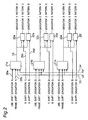
- Fig. 2 is a block diagram showing an internal
construction of a gradation register circuit in Fig. 1;
- Fig. 3 is an explanatory view showing a shift process
and an ON/OFF image of a gradation register section shown
in Fig. 2;
- Fig. 4 is a diagram showing a construction of
connecting outputs of the gradation register section shown
in Fig. 2 to each row;
- Fig. 5 is a diagram showing a dispersion arrangement
of an ON/OFF pattern in the first embodiment of the present
invention;
- Fig. 6 shows pixel arrangement examples in the first
embodiment of the present invention where (a) shows a
stripe arrangement, and (b) shows a delta arrangement;
- Fig. 7 is a diagram showing an ON/OFF pattern with
respect to the three primary colors in a gradation 1/7 in
any one frame in the first embodiment of the present
invention;
- Fig. 8 is a diagram showing another example of the
ON/OFF pattern in a gradation 1/7 in any one frame in the
first embodiment of the present invention;;
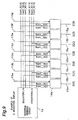
- Fig. 9 is a block diagram showing a construction of a
gradation control in the case of performing 5-gradation
display in the first embodiment of the present invention;
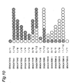
- Fig. 10 is a diagram showing a gradation register used
in the case of performing 16-gradation display in the first
embodiment of the present invention;
- Fig. 11 is an illustration showing an arrangement
relationship between a driver IC and a display section
according to a second embodiment of the present invention;
- Fig. 12 is a diagram showing an example of an
orthogonal function in the case of performing a drive by a
simultaneous selection method of 4 rows in the second
embodiment of the present invention;
- Fig. 13 is a diagram showing an arithmetic operation
of an input signal and an orthogonal function in a multi-line
simultaneous selection method in the second embodiment
of the present invention;
- Fig. 14 is a block diagram showing an insertion
position of an arithmetic section in the case of using a
multi-line simultaneous selection method in the second
embodiment of the present invention;
- Fig. 15 is a diagram showing an example of an ON/OFF
pattern in the second embodiment of the present invention;
- Fig. 16 is a diagram showing a configuration example
of a gradation register circuit for generating the ON/OFF
pattern shown in Fig. 15;
- Fig. 17 is a chart showing input signal waveforms of
control signals and register outputs in the gradation
register circuit shown in Fig. 16;
- Fig. 18 is a diagram showing another example of an
ON/OFF pattern in the second embodiment of the present
invention;
- Fig. 19 is a diagram showing a shift amount having the
least flicker in each gradation i the case of using the
gradation register shown in Fig. 10;
- Fig. 20 is a diagram showing a construction of a
display device in the case of using an active-matrix type
display device in the second embodiment of the present
invention;
- Fig. 21 is an illustration showing an ON/OFF pattern
of every frame in a gradation process according to a third
embodiment of the present invention;
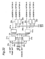
- Fig. 22 is a diagram showing an internal configuration
of a gradation register circuit in the case of performing
the gradation display shown in Fig. 21;
- Fig. 23 is a diagram showing an arrangement
relationship between the gradation register circuit and the
gradation decoding section in the case of performing a
video-signal processing as shown in Fig. 21;
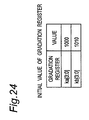
- Fig. 24 is a view showing initial values of gradation
registers in the third embodiment of the present invention;
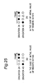
- Fig. 25 shows ON/OFF patterns by the initial values of
the gradation registers shown in Fig. 24, wherein (a) is an
explanatory view in the case of ON and OFF being continuous,
and (b) is in the case of alternating arrangement;
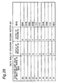
- Fig. 26 is a view showing a relationship of inputs and
outputs of the gradation decoding section in the third
embodiment of the present invention;
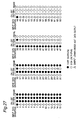
- Fig. 27 is a diagram showing another example of an
ON/OFF pattern in the case of performing a gradation
display in the third embodiment of the present invention;
- Fig. 28 is a diagram showing another example of an
ON/OFF pattern in the case of performing a gradation
display in the third embodiment of the present invention;
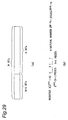
- Fig. 29 is a view showing an initial value of a
gradation register in the case of performing different
gradation displays by dividing for a M-bit input into high-order
M-N bits and low-order N bits;
- Fig. 30 is a diagram showing an arrangement example of
a gradation register section and a gradation decoding
section in the third embodiment of the present invention;
- Fig. 31 is a view showing a relationship of inputs and
outputs of the gradation decoding section in the third
embodiment of the present invention;
- Fig. 32 is a diagram showing a segment signal line
output section in the case of outputting the N-bit output
through pulse-height modulation in the third embodiment of
the present invention;
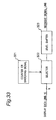
- Fig. 33 is a diagram showing a segment signal line
output section in the case of outputting the N-bit output
through pulse-height modulation in the third embodiment of
the present invention;
- Fig. 34 (b) is a waveform of a segment signal line at
the time of pulse-width modulation in the third embodiment
of the present invention, and (a) is a view showing a
comparison with a conventional example thereof;
- Fig. 35 (b) is a waveform of a segment signal line
input at the time of pulse-width modulation in the third
embodiment of the present invention, and (a) is a view
showing a comparison with a conventional example thereof;
- Fig. 36 is a block diagram showing an arithmetic
section for realizing a multi-line simultaneous selection
method in a PWM display in the third embodiment of the
present invention;
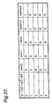
- Fig. 37 is a view showing an input/output relationship
of an adder section of Fig. 36;
- Fig. 38 (b) is an output waveform of a segment signal
line in the case of performing PWM by a multi-line
simultaneous selection method in the third embodiment of
the present invention, and (a) is a view showing a
comparison with a conventional example thereof;
- Fig. 39 is a diagram showing a relationship between
the outputs of the gradation decoding section and a
displayable gradations number with respect to 4-bit input
data according to the fourth embodiment of the present
invention;
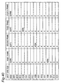
- Fig. 40 is a view showing a relationship of output
values in each frame with respect to each input gradation
in the case of performing a gradation display in the fourth
embodiment of the present invention;
- Fig. 41 is a view showing a relationship of each pulse
of PWM in a row selection period in the fourth embodiment
of the present invention;
- Fig. 42 is a view showing an input/output relationship
of a gradation decoding section in the fourth embodiment of
the present invention;
- Fig. 43 is a block diagram showing a construction from
any one column video signal to a segment signal in the
fourth embodiment of the present invention;
- Fig. 44 is a block diagram showing a construction
example of a gradation processing section in the fourth
embodiment of the present invention;
- Fig. 45 is a block diagram showing an arrangement
relationship of the gradation register circuit, gradation
decoding section, arithmetic section and selector section
in the fourth embodiment of the present invention;
- Fig. 46 is a diagram showing another example of an
arrangement relationship of the gradation register circuit,
gradation decoding section, arithmetic section and selector
section in the fourth embodiment of the present invention;
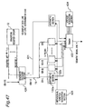
- Fig. 47 is a block diagram showing another
construction example of a gradation processing section in
the fourth embodiment of the present invention;
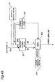
- Fig. 48 is a block diagram showing another
construction example from any one column video signal' to a
segment signal in the fourth embodiment of the present
invention;
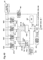
- Fig. 49 is a block diagram showing further another
construction example from any one column video signal to a
segment signal in the fourth embodiment of the present
invention;
- Fig. 50 is a block diagram showing further another
construction example from any one column video signal to a
segment signal in the fourth embodiment of the present
invention;
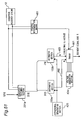
- Fig. 51 is a block diagram showing further another
construction example from any one column video signal to a
segment signal in the fourth embodiment of the present
invention;
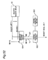
- Fig. 52 is a block diagram showing another
construction example of a gradation processing section in
the fourth embodiment of the present invention;
- Fig. 53 is a view showing an input/output relationship
of a gradation decoding section shown in Fig. 52; and
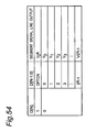
- Fig. 54 is a view showing an input/output relationship
of a voltage output section shown in Fig. 52.
-
Best Mode for Carrying Out the Invention
-
The following describes the embodiments of the present
invention with reference to the appended drawings. It is
noted that similar components are designated by the same
reference numbers in the appended drawings.
(Embodiment 1)
-
Fig. 1 shows a block diagram for outputting an ON or
OFF signal to segment signal lines 'for performing a
gradation display through a frame modulation (FRC) with
respect to a video signal input 13.
-
12 is a gradation register circuit for outputting FRC
data corresponding to each gradation, 14 is a gradation
selection section, and 15 is a display data line. As shown
in Fig. 2, the gradation register circuit 12 includes a
gradation register section 21 (21a, 21b, 21c) which
generates gradation pattern data 23 and a reference
position changing section 22 (22a to 22f). That is, there
are included registers which are different every gradation
or every different ratios of ON and OFF frames, and the
registers are shifted by bits given as a frame shift or
line shift serving as a shift amount designation signal 26
which designates an amount of shifting the registers
according to a frame shift control signal 24 or a line
shift control signal 25 every frame or every line. In the
present invention, although the explanation is made with a
shift amount when shifting to the right, a similar effect
can be obtained when shifting to the left. This is because,
(left shift amount) = (all bits number) - (left shift
amount), and this is merely a difference in numeric
expression.
-
Fig. 3 shows states of the registers to be shifted.
This shows an operation performed in the gradation register
section 21 in Fig. 2. This is a case of gradation 1/7
where a shift amount (line shift) on every line is 1 and a
frame shift is 3. For brief explanation, a shift on every
display color is disregarded, and the explanation is made
with a R output monochrome. In Fig. 3, a white circle 31
indicates an ON pixel, and a inclination-lined black circle
32 indicates an OFF pixel.
-
Since the gradation is 1/7 where one time of ON is
included in 7 frames, the register has a bit width same as
the frames number. In addition, one piece of 1 indicating
ON is included (of course, it may be also possible that ON
is indicated as 0 and the number of 1 and 0 may be
reversed).
-
After outputting the first row, the registers are
shifted rightward by an amount of a line shift
corresponding to a gradation which is a shift amount
indication signal 26 based on a line sift control signal 25.
As shown from (a) to (b) of Fig. 3, the register is shifted
by one rightward. Also, in the second to third rows, as
shown from (b) to (c), there is a shift by one in the third
row with respect to the second row. This operation is
repetitively performed from the first row to the last row.
Namely, assuming that the line shift amount is L, the
register output on the N-th row is equal to that obtained
by shifting rightward by L bits from the register output on
the (N-1)th row (where N is a natural number in a range of
2 or more and equal to or smaller than the number of
display rows).
-
Meanwhile, the change in the register outputs from the
last row of the first frame to the first row of the second
frame becomes a result obtained by changing by the frame
shift amount from the register output on the first row of
the previous frame precedent by one frame as shown in Fig.
3 (change from (a) to (d)). In general, the output of the
gradation register section 21 on the first row of the M-th
frame results in that obtained by shifting rightward by a
frame shift F from the register output of the (M-1) th frame
(where M is a natural number of 2 or more, and when M = 1,
the initial value of the register is used).
-
As described above, the reason why the shift from the
last row to the first row is different on every line is, to
securely output all the bits of the gradation register
section 21 with the frames number completing the FRC paying
attention to one pixel, and to reduce flickers by random
ON/OFF patterns by performing different shifts on every
rows and every frames.
-
In order to display the gradation 1/7, since ON occurs
one time in 7 frames, it can be securely expressed if the
7-bit outputs of the 7-bit gradation register are all in
any order outputted in the 7 frames. In order to execute
this, the shift processing of the registers is performed by
the frame shift, and the frame shift control signal 24 for
performing the frame shift is inputted every frame to
thereby perform the shift of the gradation register section
21.
-
Moreover, a frame shift was performed as a means for
spatially dispersing the ON/OFF patterns. As shown in Fig.
4, the outputs of the gradation register section 21 are
arranged in a manner such that the most significant bit is
connected as the first column and the second significant
bit is connected as the second column, and so on to the i-th
column in the case of an i-bit register. Next, the most
significant bit is again connected as the (i+1)th column,
and similarly connected in turn to the last column. Note
that this is performed on every display color. By this
arrangement, when watching the pixels on the same row, the
ON/OFF patterns of the same ratio of the display gradation
are dispersed to be displayed if the display columns number
is a multiple of the bit number of the gradation register
(in this case, it may be possible to connect to the first
column from the least significant bit, instead of
connecting to the first column from the most significant
bit).
-
Moreover, it is possible to disperse the ON/OFF
patterns by performing the line shift when paying attention
to the pixels on the same column. This can be realized by
inputting the line shift control signal 25 every one row.
In the case where a line shift is not performed, although
the ON/OFF pattern on the same column is not dispersed, by
performing the line shift, it becomes possible to display
the ON/OFF pattern at the same ratio of the display
gradation also in the column direction in the case of
performing the same gradation display on the entire screen
as shown in Fig. 5. In Fig. 5, 51 indicates a line shift
(i.e., 1 in this case), and 52 indicates a frame shift (i.e,
3 in this case).
-
By this arrangement, as shown in Fig. 5, it is
possible to disperse the ON/OFF patterns in-plane and
inter-frame. In addition, since the three primary colors
display is performed on a color panel, pixels of red, green
and blue or pixels of cyan, yellow and magenta are
generally alternately adjoined, but the ON/OFF pattern of
the pixels on a monochrome panel is shown in order to
express theeffect of the line shift and tge frame shift.
-
In addition, since the bit length of the gradation
register section 21 or the number of 1 indicative of ON are
different on every gradation, different registers are
prepared for these different gradations so that different
patterns are outputted for each gradation as shown in Fig.
2.
-
In the patterns for each gradation, as shown in Fig. 1,
each gradation is inputted to the gradation selection
section 14 one by one bit, and the patterns corresponding
to the gradation data sent from the video signal 13 are
outputted to the display data lines 15 and sent to a
display section. At this time, since the gradation 0 and
gradation 1 are always OFF or ON, it is not necessary to
spatially or time-basely disperse the pattern, and it is
possible to response under the control by the gradation
selection section 14, and therefore the patterns are not
stored in the gradation register circuit 12. By this
arrangement, the number of the input signal lines of each
of the gradation selection sections 14 can be reduced and
the circuit scale can be reduced.
-
Although the explanation is made by monochrome in the
above description, the three primary colors are used to
perform a color display in a color display device. Since
the three colors are red, green and blue in many cases, the
display device of the present invention is described using
these three colors, but similar effects can be obtained
also in a display device using three colors of cyan, yellow
and magenta. Note that the present invention can be
applied to two colors display of red, blue or the like.
Also, the present invention can be applied in the case of
four or more colors display such as red, green, blue and
yellow.
-
Although it is considered that the flickers are
reduced by shifting the ON/OFF timings of the pixels
adjoining in the same color, the adjoining pixels are
different colors in many cases in a display device
performing a color display as shown in Fig. 6. In Fig. 6,
61 denotes a pixel displaying the first color, 62 denotes a
pixel displaying the second color, and 63 denotes a pixel
displaying the third color. Even in a stripe arrangement
as shown in Fig. 6 (a) and a delta arrangement as shown in
Fig. 6(b), it is found that different colors pixels are
adjoining in more cases compared to the same color pixels.
Also, a method of laterally arranging the same color is
similar in the stripe arrangement. Of course, even in the
delta arrangement is similar.
-
The changing of the ON/OFF timings between the
different colors pixels like this is effective for further
reduction of the flickers. Therefore, as shown in Fig. 2,
difference register outputs are performed for every display
colors (for example, red, green and blue) in the same
gradation. In the example shown in Fig. 2, upon receipt of
the first register output (gradation pattern data) 23, the
register value is used as it is for the red display pixel
(referred to as "R" pixel, hereinafter), and then for the
green color display pixel (referred to as "G" pixel,
hereinafter), the output register value is shifted by a bit
number designated by the G shift (shift amount designation
signal 26c) and is outputted from the reference position
changing section 22a. Similarly, for the blue color
display pixel (referred to as "B" pixel, hereinafter), the
output register value (gradation pattern data) 23 is
shifted by a bit number designated by the B shift (shift
amount designation signal 26d) and is outputted from the
reference position changing section 22b.
-
This operation is separately performed for every
gradation, and since the values of the G shift and B shift
can be different on every gradations, it is possible to
display with further reduced flickers. In addition, the
shift processing is merely performed on the input value by
the bits determined by the G shift and B shift in the
reference position changing section 22, and therefore a
latch processing is not necessary and a register is not
necessary. The flicker occurrence degree is not different
in comparison with the case of having three colors
gradation register sections 21 for one gradation, and the
number of the registers becomes one third and therefore an
IC can be designed with a reduced circuit scale.
-
Fig. 7 shows an ON/OFF pattern of the first frame in
the case of entirely displaying the gradation 1/7 by the G
shift and B shift. In this figure, 81 denotes the G shift
(3 in this case), and 82 denotes the B shift (4 in this
case). In comparison to the case of Fig. 8 where the G
shift and B shift are not performed, the ON/OFF pattern can
be made random.
-
Although the method for suppressing the flickers was
described in the case of the gradation 1/7, flickers can be
suppressed by using the line shift, frame shift, G shift
and B shift similarly for another gradation. In general,
in the case of performing a display of J/K gradation (here
J and K are natural numbers having a relationship of J<K),
the bit width of the gradation register section 21 is K,
and it is sufficient that the number of bits indicating ON
exists J pieces among them. Though the arrangement of the
bits indicating the J pieces of ON is optional, it is
desirable that the J pieces of ON are continuously arranged
in the initial state of the register in order to reduce the
flickers by a shift processing.
-
Regarding the shift except for a frame shift, the
shift amount may be optional in a range from 0 to (K-1),
but regarding the frame shift, all of the bits of the K-bit
register are necessarily displayed one time on each pixel
without fail before completion of FRC (K frames in this
case) although the order thereof is optional, and therefore
assuming that the frame shift value is F, when a value of F
XX (X is a natural number) is equal to a common multiple,
the minimum value of X must be K or more.
-
The gradation register section 21, shift amount
designation signal 26 and reference position changing
section 22 are prepared for each gradation as shown in Fig.
2, and an ON/OFF pattern corresponding to each display
color of each gradation is outputted. The method of
outputting the output to each segment signal line is as
described in the case of the 1/7 gradation with reference
to Fig. 4, the most significant bit is connected to the
first column, the second significant bit is connected to
the second column, and so on connected to the i-th column
in the case of the i-bit register. Next, the (i+1) th
column is connected with the most significant bit again,
and thereafter connected in the order up to the last column.
-
In this manner, the register output corresponding to
each gradation is sent to each segment signal line one by
one bit. There is provided a gradation selection section
14 on each of the segment signal lines as shown in Fig. 1,
so that ON/OFF data is outputted in accordance with the
gradation of the video signal 13. Note that Fig. 1 shows
the case of performing a 7-gradation display displaying
gradations 0 to 6. The reason why there is no gradation
register corresponding to the gradations 0 and 6 is because
these gradations are all indicative of OFF or ON, and in
the case where the gradation 0 is inputted to the inside of
the gradation selection section 14 from the video signal 13,
an OFF signal may be outputted to the display data line 15
irrespective of the output of the gradation register
section 21, and in the case where the gradation 6 is
inputted, an ON signal may be outputted to the display data
line 15 irrespective of the output of the gradation
register section 21, and it is possible to deal with the
cases within the gradation selection section 14.
-
Fig. 9 shows a relationship between the gradation
register circuit 12 and the display data lines 15 when
performing a 5-gradation display. Note that the respective
gradations of the 5-gradation display are 0, 1/4, 1/2, 3/4
and 1. Note that, the third gradation may be 2/4, but the
circuit scale for shift processing becomes large due to the
bit width of the register being 4, and flickers easily
occur because of increment of the frames number performing
a FRC, and therefore 1/2 is preferable. In this manner, by
independently shift-processing each gradation, a
combination of FRC requiring frames number different for
every gradations may be used. In addition, since the
gradation 3/4 has an ON/OFF pattern inverse to ON/OFF of
the gradation 1/4, the gradation register circuit 12 is
commonly used and the gradation selection section 14 may
decide whether the ON/OFF pattern to be outputted to the
display data 15 is inverted or not. By this arrangement,
the signal lines from the gradation register circuit 12 to
the gradation selection section 14 are reduced in number,
and the registers of the gradation register circuit 12 are
reduced in number, so that the circuit scale can be reduced.
-
The outputs of the gradation register section 21
include three 4-bit outputs (Kai41_R, Kai41_G, Kai41_B)
corresponding to each display color of the gradation 1/4
and three 2-bit outputs (Kai21_R, Kai21_G, Kai21_B)
corresponding to each display color of the gradation 1/2.
to the signal line outputted to the R pixel, the respective
most significant bits of the respective gradation registers
are inputted to the segment signal line 1 as the register
output corresponding to the R pixel, and the lower bits
lower one by one bit are inputted to the segment signal
lines after the segment signal line 2 (the next of the
least significant bit returns to the most significant bit
again). The G pixels and B pixels are similarly arranged.
In this manner, the ON/OFF data patterns are outputted to
the respective signal lines.
-
Fig. 10 shows the initial values of each gradation
register in the case of performing a 16-gradation display
for each color, namely, 4096 colors display, using the
invention described above. Although the minimum necessary
frames in number for performing the 16-gradation display
were conventionally 15 frames, the present invention can
reduced to 12 frames. Moreover, though an increasing rates
of ON rate are different between respective gradations,
there is no obstacle for displaying
-
Also, when 16 gradations are displayed, in a similar
manner to the 5-gradation display, in order to reduce the
number of the gradation register sections 21, common
gradation register sections 21 are used between the
gradations 1 and 14, 2 and 13, 3 and 12, 4 and 11, and 7
and 9, having the ON/OFF ratios reversed, so that the
gradation selection section 14 determines which of ON and
OFF is taken based on the input data when the value of the
gradation register section 21 is 1, thereby reducing the
circuit scale. By this arrangement, it becomes possible to
perform a gradation display under the FRC.
(Embodiment 2)
-
In a simple matrix type liquid crystal display device,
when performing a drive using a liquid crystal of a highspeed
response characteristic for displaying a moving
picture, there is a problem that contrast deterioration
occurs due to a frame response.
-
As a method for solving this, a multi-line
simultaneous selection method (Multi Line Selection Method:
MLS) was proposed. In this method, common signal lines of
multi lines (L rows) are simultaneously selected to apply a
scanning voltage, and at the same time voltages in
accordance with corresponding data are applied from the
segment signal lines. This operation is performed until
all of the common signal lines are selected, and further
selection signals are applied at least L times from the
common signal lines to one frame. Since the signals can be
selected L times in one frame, it is possible to prevent
the contrast from deterioration due to a frame response
-
In addition, in a conventional line-sequential drive,
in the case where 240-line display is performed using a
liquid crystal having an ON voltage of 2.5 V, a voltage of
the common signal line is 26.49 V and a voltage of the
segment signal line is 1.71 V, and a voltage difference
between the two signal lines is large. In the multi-line
simultaneous selection method, the common signal line
voltage is 26.49/L½ (V) and the common signal line voltage
is 1.71×(L½(V), so that the voltage difference between the
common signal line and the segment signal line is reduced,
and thus a circuit of the common signal lines and the
segment signal lines can be designed in the same chip.
Accordingly, as shown in Fig. 11, a driver IC 192 is
mounted only at one side of a display section 193 on an
insulation substrate 191, and the remaining three sides
have no IC provided, to be advantageous that the display
section is allowed to be placed symmetrically with respect
to an equipment.
-
In the present invention, the gradation display was
performed using a 4-rows simultaneous selection method (MLS
4). A voltage value in one frame period of each row of the
common signal lines is decided by an orthogonal function
shown in Fig. 12. The number of columns of this orthogonal
function is equal to the number of the common signal lines,
and the common signal line on the first column takes the
first column values of the orthogonal function from the
first row in the order in one frame to thereby output a
voltage value corresponding to the data. Thereafter, the
values of the second column indicate a change of the common
signal line voltage of the second row, and teh number of
the columns indicates teh number of the common signal lines.
Meanwhile, time (sequence) is shown with respect to the row
direction and one frame period is shown by the time ranging
from the first row to the last row. Accordingly, the time
of applying for one value is equal to (one frame period) /
(rows number). Note that the present invention is not
limited to the 4-row simultaneous selection method. For
example, 2-row simultaneous selection method (MLS 2) may be
used. That is, the present invention is applicable to any
method of simultaneously selecting a plurality of rows.
-
Namely, the column corresponds to a change in time of
a voltage waveform applied to the common signal line, and
the row corresponds to the voltage waveform applied to the
common signal line of the display device at one time.
-
Each element applies to the common signal line a
positive selection pulse when 1, negative selection pulse
when -1, and non-selection pulse when 0.
-
Meanwhile, the voltage applied to the segment signal
line is given by a multiplication result between a matrix
of the input signal lines as shown in Fig. 13 and a matrix
H of the orthogonal function shown in Fig. 12.
-
The input signal S121 has ON/OFF data corresponding to
one frame, and is a matrix using binary values of -1 and 1
where -1 is ON and 1 is OFF. In addition, the number of
rows is equal to the number of common signal lines, and the
number of columns is equal to the number of the segment
signal lines.
-
A voltage of five values is applied in accordance with
the arithmetic result of H×S. The column corresponds to
the number of the segment signal lines and the row
corresponds to a time change of each of the segment signal
lines.
-
The ON/OFF display of the pixels is performed in
accordance with the voltage value applied in this manner
between the segment signal lines and the common signal
lines.
-
In order to calculate a voltage to be applied to the
segment signal line at one time, respective elements of one
row of the orthogonal function H125 and one column of the
input signal S121 are required. Herein, as shown in Fig.
12, 0 is included in one row of the orthogonal function
H125 except for 4 pieces, by taking an advantage of the
fact that the arithmetic operation with the elements of the
input signal S121 corresponding to 0 is always 0, a matrix
calculation is performed between the pixel data performing
the row selection and the elements of the selection signal.
Thus, the circuit and time required for the calculation are
reduce. Accordingly, in order to perform the segment
signal output by the H×S matrix calculation, data of four
rows amount is sent from the gradation selection section 14
and is multiplied with the orthogonal function in turn, and
thereafter the sum of the data of four rows amount may be
outputted. In addition, since a video signal is generally
sent from upper or lower row in turn in a display region in
many cases, it is desirable that the selected four rows. are
continuous four rows.
-
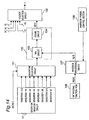
Fig. 14 shows a gradation register circuit 12, a
gradation selection circuit 131, an arithmetic section 132
for performing a drive by the MLS, and a voltage selection
circuit 135 for outputting a segment signal line voltage in
accordance with the arithmetic result. Here, an inversion
processing circuit 137 is provided for exchanging between a
positive selection pulse 1 and a negative selection pulse - 1
for applying an AC voltage to the display section.
-
After the data of four rows is sent from the gradation
selection circuit 131 to the arithmetic section 132, there
is an output from the arithmetic section 132, and therefore
the data transfer from the gradation selection circuit 131
to the arithmetic section 132 may be performed either by a
transfer at a transfer rate four times thereof or by a
parallel transfer by simultaneously processing the four
rows. In the present invention, an example of processing
is described in the case of transferring at the four times
of transfer rate.
-
The shift-processing was performed in the gradation
selection circuit 131 and the gradation register circuit 12,
and a gradation display was performed in the MLS drive
under the FRC.
-
As a result, when V2, Vc or -V2 of the five values of
the segment signal lines (voltage values V2(=2×V1), V1, Vc,
-V1, -V2 in the descending order) is displayed, flickers
and stripe-like unevenness along the segment signal line
were conspicuous.
-
In the four-rows simultaneous selection method (MLS4),
which voltage of the segment five values should be taken is
decided based on the calculation between the input signal
S121 and the orthogonal function H125 as shown in Fig. 13.
the voltage values V2 in the case of the calculation result
being 4, V1 in the case of 2, 0 in the case of 0, -V1 in
the case of -2, and -V2 in the case of -4 are taken. When
the orthogonal function H125 is given as shown in Fig. 12,
in the case of the calculation result being ± 4 or 0, the
ratio of the ON and OFF pixels is 3:1 or 1:3 in the four
pixels simultaneously selected.
-
When the ON/OFF pixels are dispersed as performed in
Fig. 7, the ratio of ON and OFF pixels is apt to be 1:3 or
3:1 whens paying attention to the continuous four rows
(herein the rows are scanned in order from the first row).
Especially, it is apt to be one of the gradation register
sections 21 which turns ON (or OFF). In order to prevent
this, there is a method of arranging the line shift values
having the ON (or OFF) pattern located on the same column
every two lines. In this method, there is a limit in
values to be taken of the line shift, and the ON (or OFF)
pattern is not located on the same column every two lines
in such as a gradation 1/7 even if the line shift value is
adjusted.
-
Therefore, the same ON/OFF pattern with even two rows
and the same ON/OFF pattern with odd two rows are made
among the simultaneously selected four rows, so that the
ratio of the ON and OFF pixels is 2:2 or 4:0 (0:4)
irrespective of the shift amount, and thus the flickers and
stripe-like unevenness along the segment signal line were
reduced.
-
Fig. 15 shows an ON/OFF pattern in the case of a
gradation 1/7 of only R pixels. In this example, the
explanation is made assuming that the common signal lines
are selected every four rows from the first row in order.
That is, the signal lines from common 1 to common 4 are
first simultaneously selected, and then the lines of
commons 5 to 8 are selected in the next period. When
paying attention to the commons 1 to 4, the ratio of the ON
and OFF pixels is 2:2 or 0:4 in the simultaneously selected
four rows in each column, and therefore the voltage to be
applied to the segment signal line is ± V1. In the G
pixels or B pixels, since this pattern is merely shifted
rightward (or leftward) entirely, the voltage to be applied
to the segment signal line is ± V1 either in the G pixels
or B pixels.
-
The shift changing the pattern of the even number rows
among a set of the four rows to be simultaneously selected
is even/odd shift 53. The line shift 51 is executed every
change of a set of the four rows. A frame shift 52 is an
amount of shifting the pattern in comparison with the
previous frame pattern every change of the frame as is
before.
-
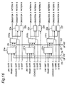
In order to realize the ON/OFF pattern like this, the
configuration of the gradation register circuit 12 is
changed from that shown in Fig. 2 to that shown in Fig. 16.
The different points from Fig. 2 are that, in addition to
the line shift control signal 25 and frame shift control
signal 24 serving as one of the control signals for
performing shift-processing of the registers, an even/odd
shift control signal 152 is provided, and whereas the line
signal control signal 25 generates a pulse every one row of
the input video signal to perform a shift process in Fig. 2,
the pulses are generated every four rows which the number
is the number of the simultaneous selection rows and
further a pulse is generated every one row on the even/odd
shift control signal 152.
-
In addition, even/odd shift processing sections 151
are provided, and only when the outputs of the gradation
register section 21 correspond to the even rows data among
a set of four rows, the registers are shift-processed in
accordance with the even/odd shift values.
-
Fig. 17 shows an input video signal and each of the
control signals, and register pattern. In the gradation
register section 21, when the frame shift control signal
(FSF) 24 is inputted, the gradation register is shift-processed
based on the frame shift amount. In addition,
when the line shift control signal (LSF) 25 is inputted in
the case of FSF 24 being not inputted, the gradation
register is shift-processed based on the line shift amount.
The frame shift for every frame and line shift for every
four rows are thereby realized.
-
The even/odd shift-processing is performed in the
even/odd shift-processing section 151 to detect the even
number rows among the four rows simultaneously selected by
the even/odd shift-processing signal (ASF) 152, and when
the gradation pattern data 23 corresponding to the data of
the even number rows is inputted, the gradation pattern
data 23 is shift-processed in accordance with the even/odd
shift value. In the case of the gradation pattern data 23
corresponding to the data of the odd number rows, the shift
processing is not performed and the register is outputted.
-
The gradation pattern R is thereby outputted as shown
in Fig. 17 in the case where the line shift is 1, frame
shift is 3 and even/odd shift is 2 in the case of, for
example, 1/4 gradation.
-
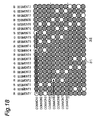
Fig. 18 shows an ON/OFF pattern in one frame when
performing a 1/7 gradation display for all of the three
primary colors. Since the ON/OFF pattern is not 1:3 or 3:1
in the simultaneously selected four rows (commons 1 to 4,
commons 5 to 8 and the like), ±V2 and Vc are not outputted
and flickers and unevenness which may occur along the
segment signal line can be reduced.
-
Fig. 19 shows values of the respective shift amounts
when performing every color 16-gradation display (4096
colors display) using the gradation register shown in Fig.
10. When the shift like this is performed and the
gradation control is performed under the FRC, it is
possible to realize a display with few flicker at a frame
frequency of 75Hz.
-
In the pattern of Fig. 18 compared to the pattern of
Fig. 8, parameters for performing a shift are increased,
and therefore the ON/OFF pattern can be made more random,
so that a display with few flickers can be possible even at
a low frame frequency.
-
The modified point for realizing the pattern of Fig.
18 is, as described with reference to Fig. 16, merely to
increase a signal for controlling a shift amount by one and
to provide the even/odd shift-processing section 151, and
it is not always necessary to employ a multi-line
simultaneous selection method. Execution is possible also
in the conventional line sequential drive. In that case,
the arithmetic section 132, orthogonal function ROM 136 and
the like shown in Fig. 14 are not necessary, and it is only
necessary to output the output of the gradation selection
circuit 131 to the segment signal lines.
-
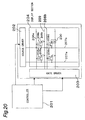
As shown in Fig. 20, a gradation display under the FRC
according to the present invention is possible also in an
active matrix type display device using such as a thin film
transistor (TFT). For example, this can be realized by
outputting a voltage value corresponding to ON/OFF data
outputted to the display data line 15 in accordance with a
potential of an opposite electrode 209 in a source driver
202.
-
Moreover, as a display element, the present inveniton
can be applied to not only a liquid crystal but also any
display element which can express binary states of ON and
OFF such as an organic light-emitting diode (OLED), light-emitting
diode (LED), inorganic electro-luminescence (EL)
element, plasma display panel (PDP), electric-field
emission display (FED), and the like. Of course, if such
as a MLS system is employed, the present invention can be
also applied to a display element (display) which can
express a state of 2 or more values.
-
Though the explanation is made as to the case of four-line
simultaneous selection method of the multi-line
simultaneous selection method, since L rows of the image
data can be simultaneously transferred also generally in an
L-line simultaneous selection, and therefore similar
effects can be obtained by changing the pattern at every
row.
-
If the display gradation number is increased by multi-coloring,
the number of frames required for gradation
display is increased in a gradation display under FRC, and
flickers are easily generated. In order to suppress the
occurrence of the flickers, it is necessary to increase the
frame frequency. However, since the increase of the frame
frequency results in increase of electric power consumption,
it is desirable to drive at a possibly low frequency.
-
Therefore, a display is performed by a combination of
a gradation display method under FRC with a pulse-width
modulation method (PWM) or a pulse-height modulation method
(PHM).
-
In this method in comparison to performing a gradation
display using only the PWM, since the notching number of
the pulse in one period is reduced, an effect of brightness
difference due to waveform corruption caused by a
resistance and floating capacity of a signal line or by a
floating capacity of a load can be reduced to be
advantageous.
-
In addition, in comparison to performing a gradation
display using only a PHM, since the number of the voltage
values required for the segment signal lines is reduced, a
notching width between the gradations is increased so that
an effect of a gradation inversion due to differences in
output preciseness can be reduced. Moreover, it is also
possible to delete an output digital-analogue converter and
to selectively output one of the necessary voltage values
by a selector.
(Embodiment 3)
-
Fig. 21 shows a method of performing a gradation
display using FRC together with PWM (or PHM) referring to
6-bit signal.
-
As shown in Fig. 21(a), assuming that, with respect to
the 6-bit input, the more significant 2 bits are FRC-processed
and the less significant 4 bits are subjected to
PWM or PHM, since the FRC process is performed with 2-bit
data, the number of frames required for FRC is three frames.
The number of frames having ON and OFF among this is
determined by the 2-bit data, so that an ON/OFF pattern
like three frames shown by 211 in Fig. 21(b) is obtained.
Note that a shift process for reducing flickers is not
considered here and only a rate of ON and OFF is described.
In fact, the frames to be ON are different according to
pixels.
-
Next, the less significant 4-bit data is outputted as
it is using one frame (212 in Fig. 21(b)).
-
By this arrangement, since four ways of gradations due
to difference of the FRC and further sixteen ways of
gradations due to the frames of 212 are respectively taken,
it is possible to perform 64-gradation display.
-
Note that, this method is not limited to 6-bit input
and is also executable to M-bit data, and PWM or PHM is
performed with the less N significant bits (here M>N) and
FRC is performed with the more significant (M-N) bits, so
that displays of 2M-N gradations under FRC and 2N gradations
under PWM or PHM respectively to a FRC pattern can be
performed, and therefore 2M gradations display can be
performed.
-
Note that, referring to N value, M>N>0 is preferable,
but when N is small, the number of frames is increased and
the frame frequency is required to be raised for preventing
flickers, and moreover there appears a gradation difference
because of decrease of a horizontal scanning period due to
increase of the frame frequency and decrease of one pulse
width, and therefore a result of M-N<4 is desirable. At
this time, since a 16-gradation display is performed under
FRC, the display at a frame frequency of 75Hz can be
performed using the flicker processing method and teh
gradation registers described in Embodiments 1 and 2.
-
Figs. 22 and 23 show a method of realize the pattern
as shown in Fig. 21 and a method of varying an ON/OFF
pattern by the pixels within the same frame. The
explanation is made here in the case where the video signal
13 is 6 bits and 16 gradations are expressed through PWM or
PHM. The number of frames required for expressing the
entire gradations is four frames as shown in Fig. 21(b).
Accordingly, the bit length of the register stored in the
gradation register section 21 is 4 bits.
-
In Fig. 23, in the case of the more significant 2 bits
value of the video signal 13 being 0, only 1 bit amoung 4
bits is assumed to be 1 and the remaining 3 bits are
assumed to be 0. The less 4 bits of the video signal 13
are outputted onto the display data lines 15 when 1. 0
indicative of OFF of FRC is outputted when 0. In the case
where the value of the more significant 2 bits of the video
signal 13 is 3, the less 4 bits of the video signal 13 are
outputted onto the display data lines 15 when 1, and 15
indicative of ON of FRC is outputted when 0. The gradation
register section 21 used at this time is assumed to be a
register ka.
-
In the case where a value of the more significant 2
bits of the video signal 13 is 1 or 2, three patterns are
generated in the 4 frames, i.e., outputting ON, OFF and the
less significant 4 bits of the video signal. Accordingly,
in order to determine the three patterns, three values of 0,
1 and 2 are necessary as the register values, and the
gradation register section 21 is required to have a double
bit width or to refer to two gradation register outputs.
-
If the gradation register section 21 has a double bit
width, the circuit scale is increased due to increase of a
latch portion and a shift-processing section. Also, the
number of wirings from the gradation register circuit 12 to
the gradation decoding section 231.
-
Therefore, in order to reduce the circuit scale, two
gradation registers are used when performing the FRC of
three values, and one of the gradation register sections 21
uses a register ka, and one gradation register is commonly
used between different gradations. Thus, when the more
significant 2 bits are 1 or 2, the process is performed
using the register ka and register kb. In this method, as
the gradation increases by one, the gradation register
increases only by one, and therefore this is effective for
reducing the circuit scale.
-
In order to realize the pattern shown in Fig. 21(b),
the register kb has 2 bits to be 1 and 2 bits to be 0, and
in the case where the more significant 2 bits are 1, OFF is
outputted when the register ka and register kb are 0, and
ON is outputted when the register ka and register kb are 1,
and the less significant 4 bits of the video signal are
outputted when the values of the register ka and register
kb are different. Fig. 24 shows initial values of the
gradation registers ka and kb. In the register kb, 0 and 1
are alternately arranged different from the case of
Embodiments 1 and 2. This is because the value of the
frame shift is only 1 or 3 due to 4-bit register, and is 1
and 0 are continually arranged, two times of ON or OFF are
generated in the continuous frames as shown in Fig. 25(a).
By an alternate arrangement, as shown in Fig. 25(b), ON and
OFF can be generated on alternate frames. By the
arrangement, in consideration under FRC of two values, this
approximates to the FRC completed with two frames, and the
frame frequency can be reduced. Fig. 26 shows an
input/output relationship of the gradation decoding section
231.
-
In this case, each of the shift amount of the
registers ka and kb must be always equal. This is because
two registers are referred to in the case of the more
significant 2 bits being 1 or 2, and the numbers of OFF, ON
and the less significant 4 bits outputs are not changed.
-
Fig. 22 shows an inside of the gradation register
section shown in Fig. 23. In comparison with the
configuration shown in Fig. 16, the shift amount indication
signal 26 for the gradation register section 21 is common
to all of the registers.
-
As shown in Fig. 24, the fact that the initial value
of the register kb is 1010 is equivalent to the arrangement
having two of two 2-bit register values paralleled.
Therefore, it may be possible that the register kb is
modified from 4 bits to 2 bits to have its initial value of
10 so as to shift-process the register as much as the
register ka. Also, regarding the wirings of the gradation
display section in Fig. 23, kb[2] is replaced by kb [0] and
kb [3] is replaced by kb [1], whereby the same value as that
at the time of 4-bit register can be inputted to the
gradation decoding section 231.
-
By this arrangement, the 4-bit shift-processing is
changed to the 2-bit shift-processing in the register kb,
so that the circuit scale can be reduced. In order to
equalize the shift amounts both in the registers ka and kb,
it may be arranged that, when the shift amount of ka is 0,
1, kb is also set to 0, 1, and when the shift amount of ka
is 2, the shift amount of kb is set to 0, and when the
shift amount of ka is 3, the shift amount of kb is set to 1.
-
Although the gradation 24 and gradation 40 are
described with reference to Fig. 25, all of the gradations
16 through 47 referring to a register value kb similarly
represent effects of reducing flickers. Similarly, in this
case, OFF of two frames existing in the gradations 16 to 31
and ON of two frames existing in the gradations 32 to 47
can be dispersed by changing the initial value of the
register kb, and therefore the flickers can be reduced.
-
Fig. 27 shows ON/OFF patterns of every frame in eaach
gradation in one pixel when performing 64 gradations using
a configuration of Figs. 22 to 24 and 26. In the
gradations 0 to 15, data different from OFF is outputted in
one frame of four frames. This different data draws near
to ON 15 as the gradation rises, while data near OFF is
generated when the gradation is small, and therefore
flickers are remarkable as the gradation rise higher.
Similarly,' in the gradations 48 to 63, flickers are
remarkable as the gradation is smaller. In the gradations
16 to 31, ON/OFF/any value of 0 to 15/OFF is displayed. As
the gradation rises, the display draws near to a FRC of two
frames completion as ON/OFF/ON/OFF, and therefore the
flickers become unremarkable. Similarly, in the gradations
32 to 47, as the gradation is lowered, the flickers become
unremarkable. Therefore, the most remarkable gradations
are 15, 16, 47 and 48 among the entire gradations. These
gradations are completed under the 2-state FRC and four
frames. Accordingly, the frame frequency eliminating
flickers is 60Hz similarly to the 4-frame FRC.
-
At this time, the frame shift value is 1, line shift
value is 3, even/odd shift value is 1, G shift value is 3
and B shift value is 1. Fig. 28 shows an ON/OFF pattern in
one frame.
-
In the case of performing a display only by a pulse-width
modulation, there occurs a crosstalk in some segment
signal line voltages, and a gradation display only under
FRC requires 180 Hz, and accordingly a crosstalk-less drive
of a low power can be realized by a combination.
-
In addition, in the case where a 4-bit display data
line 15 outputted from the gradation decoding section 231
like this is outputted to a segment signal, even if 16
gradations are displayed by a pulse-width modulation or a
pulse-height modulation, there is no effect in occurrence
of flickers.
-
Generally, with respect to a video signal of M bits,
which is separated into more significant M-N bits and less
significant N bits, as shown in Fig. 29(a), in the case
where a gradation display is performed under FRC using 2M-N-1
frames and further a gradation display is performed by a
PWM or PHM within one frame, the gradation register circuit
12 requires at least 2M-N-1-1 registers as shown in Fig. 30.
These registers are designated as Register 0, Register 1
and Register 2 in the order from fewer pieces of 0. Bit
lengths of each of the registers are all in the same length
where 0 and 1 are arranged in Register X as shown in Fig.
29(b).
-
Fig. 30 shows a relationship between the gradation
register circuit 12 and the gradation decoding sections 231.
In Fig. 30, since only pixels of the same display color are
displayed, only one output is described among three
registers corresponding to the three primary colors outputs.
-
For a video signal 13 of M bits, the more significant
M-N bits data is referred as shown by the gradation
decoding section 231 in Fig. 31, and in accordance with the
output of the gradation register corresponding to each of
the segment signal lines corresponding to the data, it is
selected as to whether the N bits outputs are all set to 0,
1 or values of the more less significant N bits are
outputted.
-
The gradation register circuit 12 has a configuration
similar to that of Fig. 22, and a difference is mere that
the number of the registers and the output bit widths of
the registers are different. The shift amount designation
signals 26 of all the registers have the same value among
the registers. Note that if the values of the line shift,
frame shift, even/odd shift, G shift and B shift are the
same of all the registers, each value can be freely
established.
-
In order to reduce the number of the frames required
for FRC for suppressing flickers, the bit length of the
gradation register can be reduced, but in this case,
regarding a gradation register X and a gradation register
X-1, it is necessary that a bit length of one of the
registers can be just divided by a bit length of the other
register and the quotient must be an integer. As to a
shift amount of a gradation register having a bit length
reduced, when the shift amount exceeds the bit number, a
value obtained by subtracting the bit length from the shift
amount is used. If the value exceeds the bit number even
in this case, the subtractions by a bit length are repeated
until a value smaller than the bit number is obtained,
which is used as the shift amount of the gradation register.
-
The display data line 15 serving as a N-bit output
signal of the gradation decoding section 231 is applied to
a segment signal line by PWM or PHM to thereby perform a
gradation display.
-
As to selection of using PWM or PHM, there is no
difference in a degree of flicker occurrence but a
configuration is varied according to a driving method. For
example, when performing PWM in an active matrix type
display device, it is necessary to store data by a number
of pulses counted by PWM in a row-selection period for
every pixel, resulting in reduction of a scanning time of
one row. In addition, there is a problem that, if a
waveform becomes uneven due to such as a wiring capacity, a
predetermined signal can not be stored in a pixel.
Moreover, there is a method of performing a row scanning at
random in order to increase the scanning period, but a
construction of a gate driver is complicated. Accordingly,
it is preferable to perform a gradation display using a PHM
system.
-
In addition, in the case where a gradation display is
performed by PHW as shown in Fig. 32, in response to a
display data line 15 of N bits, there is a method in which
an analog signal is obtained using a digital-to-analog
converter to be outputted to a segment signal line 207, and
in the case of, for example, N=4, there is such a method in
which voltages of 16 values are prepared in accordance with
gradation characteristics of display elements, so that one
of the 16-value voltages is outputted to the segement
signal line 207 by operating a selector 311 in accordance
with the display data line 15. By incorporating these
functions into the source driver 202 shown in Fig. 20, a
gradation display method according to the present invention
can be realized in the active matrix type display device.
Note that the source driver 202 may be formed on the same
substrate as the display section 204 using a low
temperature or high temperature polysilicon. Of course,
also the gate driver can be formed using a polysilicon
technique. This matter can be also applied in a simple
matrix type display device.
-
In the case of a passive matrix (simple) type display
device, when a gradation display is performed by PHM by
varying the voltage value of the segment signal line, it is
necessary to apply a compensation parameter in order to
make an effective value of a non-selection pixel, and
therefore the circuit is complicated. Therefore, it is
preferable to use a PWM system.
-
In order to use the PWM system, there is a method for
dividing ON state periods and OFF state periods by dividing
a pulse applied to the segment signal line in one
horizontal scanning period into e.g. 2 N pieces or by
dividing the pulse by a number of bits in accordance with
the weight of each signal line bit. Thus, it is possible
to perform a 2N-gradation display for N-bit data.
-
In response to a display data line 15 of N bits, as
shown in Fig. 33, ON/OFF data of each bit is detected by a
selector 322, so that the ON/OFF data of one bit is
outputted by using a counter or a switching signal 321
based on ON/OFF information of each bit in accordance with
the weight of the bit.
-
Moreover, the data is converted into a voltage value
required for a display element through a level shifter 323
so as to be outputted onto the segment signal line to
thereby display ON/OFF in accordance with the voltage value
applied between common signal lines.
-
A display device is generally a capacitive load, and
when a pulse is applied, a waveform rounding is watched at
the rising and trailing times. In addition, repetition of
ON and OFF is to perform charge and discharge of an
electric charge to and from a panel, as the repetition of
ON and OFF increases, a consumption of electric power
increases and is remarkable as the pulse number increases.
Therefore, the pulses indicative of ON and pulses
indicative of OFF are adjoined as much as possible, and in
order to constitute a display device in which agradation
performance is increased with reduction of an electric
power consumption by reducing a difference of brightness of
a display region due to the waveform rounding and by
reducing the times of charges and discharges to the display
device due to repetition of ON and OFF, the pulses are
applied in the order from higher or lower segment 5-value
voltages.
-
Therefore, as shown in Fig. 34(b), the pulse is not
applied to the segment signal line in the order
corresponding to each bit data but the pulse is applied in
the order of the voltage values so that the charging times
are reduced. Fig. 34(a) shows a conventional case as a
comparative example where a pulse is applied in the order
of the pulse width.
-
As a method for preventing this, in the present
embodiment, as shown in Fig. 35(b), the pulse applicaiton
order is differentiated every segment signal line and the
timings of changing voltages of the segment signal lines
are shifted so that the differential waveform is not
applied to the common signal line.
-
In the case of performing a drive by MLS, the
obtainable voltage value of the segment signal line is a
number of simultaneous selection rows + 1. In the 4-row
simultaneous selection time, voltage values of 5 values are
generated. Accordingly, application of pulses in the order
of the voltage values is effective for reducing the
charging times.
-
In the case of performing a display by MLS, an
arithmetic unit is required for calculating data
corresponding to a number of rows simultaneously selected
below the display data line 17, and it is necessary to
modify the configuration.
-
Fig. 36 shows a block diagram from the arithmetic
section to the segment signal line output in the case where
the bit width of the display data lines 15 is 4 bits and in
the case of performing a 4-row simultaneous selection.
-
Although the display data lines 15 of 4-bit data are
arranged in parallel corresponding to four rows, the four
rows may be serially transmitted. In this case, a latch is
required in an Ex-NOR 351 or Adder 352.
-
In the case of performing a gradation display by PWM,
in response to an input signal of a plurality of bits, a
MLS calculation is performed every bit of the same weight,
and the output period of the calculation result is varied
in accordance with the weight of the bits to thereby
realize the display.
-
A calculation required for MLS, which is a matrix
calculation H × S between the orthogonal function H125 and
the input signal S121 performed in Fig. 13, is a
multiplication between elements 1 or -1 of the orthogonal
function and the data 1 or -1 corresponding to the elements.
Since the calculation is performed every bit, the even case
of an input signal being N bits is the same, and the
arithmetic sections are merely N pieces (alternatively, may
be serially processed at a rate of N times higher). When 1
and -1 of the orthogonal function are decoded to 0 and 1,
respectively, and -1 (indicative ON) and 1 (OFF) of the
input signal are decoded to 0 and 1, respectively, the
multiplication between the 1-bit signals results in equal
to an exclusive NOR. This is performed in the Ex-NOR 351.
Since there are four numerals with which the orthogonal
function becomes 1 or -1 in the 4-rows simultaneous
selection method, four results of the exclusive NOR are
outputted (as q1, q2, q3 and q4). Next, the four
calculation results of the exclusive NOR are added and one
of the five values of the voltages is outputted in
accordance with the calculation results. This addition is
executed by Adders 352. The voltages of -V2, -V1, Vc, V1
and V2 are allocated in the order from the smaller value of
q1+q2+q3+q4. Note that the outputs of the display data
lines 15 are used as the elements of the input signal S121
in Fig. 14.
-
The outputs of the four Adders 352 may be outputted to
the segment signal line in accordance with the weight of
the bits. In this case, with respect to the output period
of Adder 352d which is a calculation result of the least
significant bit, Adder 352c is made twice, Adder 352b is
made four times, and Adder 352a is made eight times so as
to be outputted in this order.
-
In this method, however, the segment signal lines are
not always outputted in the voltage order. In order to
modify to the voltage order, it is necessary to detect the
output value of each Adder 352 to selectively output.
-
By detecting the outputs of Adder 352 and based on the
detection results, the time for applying each of the
voltage values is determined, and a Selector 354 is
provided for outputting to the segment signal line.
-
Conventionally, there was employed a method that the
Selector 354 of selects one of the five voltages -V2 to V2
according to the values 0 to 4 of the Adder 352 to output
the segment signal voltage, in this method, however, if the
voltage waveforms are applied to the segment signal line in
the voltage order, all of the values of the outputs of the
Adder (outputs of four Adders in Fig. 36) of each bit are
referred to, and rearranged in- the order of the voltage
values and the output times to the segment signal line are
changed in accordance with the weight of the bits. Since
this requires to repeat this algorithm every voltage values
of -V2 to V2, the circuit scale becomes considerably large
as the bit number inputted to the selector increases.
-
In order to simplify the configuration of the Selector
section, though the original output of the Adder 352 is 2
bits, the bit number is changed to 5 bits which is a number
of employable voltage values. Fig. 37 shows a relationship
of the input/output of the Adder 352. The outputs of 5
bits correspond to the voltage values to be applied, and
only one bit thereof is 1 according to the calculation
results of q1+q2+q3+q4 and the remaining four bits are 0.
Regarding each output of the Adder 352, when paying
attention to e.g. swv2, the swv2 of the four Adder sections
352a to 352d is inputted to the Selector 354 as the 4-bit
width. At this time, each bit value of a bus of swv2[3:0]
is determined in the order of the calculation results of
the most significant bit of the input data. The remaining
four outputs are also similarly treated. Fig. 36 shows a
connections from the Adder 352 to the Selector 354.
-
Thus, in the Selector 354 five 4-bit signals are
referred to in the order from swv2 or swmv2 to thereby
decide the time for applying the voltage to the segment
signal line, so that the circuit construction of the
Selector 354 can be simplified.
-
Fig. 38(b) shows an example of the output voltage
waveform of the segment signal line in the case of using
the configuration shown in Fig. 36. In comparison to a
conventional configuration (Fig. 38(a)), the times of
voltage changes can be reduced and the electric power for
charge of the segment signal line voltage can be reduced.
-
In the above description, although the explanation is
made in the case of 4-line simultaneous selection method in
the multi-line simultaneous selection method, since image
data of L rows are simultaneously transferred also in a
general L-line simultaneous selection, the inputs of the
Ex-NOR 351 become L lines, and also the calculation results
become L pieces of q1 to qL, and also the output signal
lines of the Adder sections become L+1 lines because the
obtainable values of the segment signal voltages are L+1
pieces. That is, general L-row simultaneous selection can
be also realized, similarly.
-
Note that, as a display device, not only a liquid
crystal but also an organic light emitting element (OLED),
plasma display panel, inorganic EL element and the like so
long as the display device performs a plurality gradation
expressions, the display device can be realized by applying
the present invention similarly to the gradation display
section.
(Embodiment 4)
-
In the gradation display method of the present
invention, when inputting e.g. 6 bits as shown in Fig. 27,
the same brightness is obtained on the boundary between two
gradations where different FRC processes are performed. In
Fig. 27, pairs of gradations 15 and 16, 31 and 32, and 47
and 48 are the cases.
-
Namely, the gradations are reduced by the number of
the boundary lines. This coincides with the number of the
frames to be subject to FRC, and since 2M-N-1 frames are
used in FRC if a N-bit display is performed through PWM or
PHM in general at the time of inputting M bits, this means
that 2M-N-1 gradations are reduced with respect to 2M
gradations.
-
For example, if a display is performed with 4 frames
at the time of inputting 6 bits, 64 gradations become 61
gradations. In this case, even if a portrait or the like
is displayed, the reduction in gradations can not be
confirmed from the picture. Meanwhile, if a display is
performed with 4 frames at the time of inputting 4 bits,
the gradations become from 16 to 13 in gradation display,
and the reduction in gradation number can be confirmed in
watching even such as a portrait.
-
As a reason of decreasing the display gradations, an
explanation will be made using an example when performing
the gradation expression with four frames at the time of
displaying 64 gradations. Fig. 27 shows ON/OFF patterns of
each gradation of input 64 gradations. When paying
attention to the gradations 15 and 16, the ON/OFF pattern
of the gradation 15 become less significant output (15),
OFF(0), OFF(0), and OFF(0) (where the values in parenthesis
are 4-bit values outputted from the gradation decoding
section). Regarding the 16 gradations, which become ON(15),
OFF(0), less significant 4-bit output (0), and OFF(0), and
4-bit output values are the same among four frames between
the two gradations, and therefore the corresponding output
gradations are reduced. In Fig. 27, also between the other
gradations 31 and 32, and gradations 47 and 48, similarly,
the outputs are the same with respect to different input
gradations. Such a phenomenon is generally generated
between gradations before and after the more significant M-N
bits values are varied. As a result, the output
gradations are reduced by an amount of 2M-N-1 gradations
compared to the input.
-
An examination was carried out regarding a method of
preventing such a reduction in gradations number mentioned
above. In this description, an explanation is made with
respect to the case of performing a gradation display with
4 frames using input 4 bits for brevity. Fig. 39(a) shows
the output values of the gradation decoding section 231 in
each input gradation. In this case, the frames 1 to 4 are
allocated for the convenience, and it is sufficient to
select one time each frame of 1 to 4 among the four frames
and the order may be changed.
-
By performing such decode outputs, the pulse widths of
each of the frames are in a relationship as shown in Fig.
39(b). Since three frames of four frames take a value of
either 0 or 3 in the entire gradations, only pulses having
a pulse width 3 are prepared for the three frames, and
since the remaining one frame takes any value of 0 to 3,
two pulses having pulse widths 1 and 2 are prepared.
Accordingly, only 13-gradation expression from 0 to 12 can
be performed using four frames by ON/OFF of each pulse.
This is because the sum of the pulse widths of each frame
is 3+3+3+2+1=12.
-
In order to perform a 16-gradation expression, the
pulse width 3 is changed to 4 in the three frames of a
pulse width 3 only. As to the remaining one frame, it is
sufficient to prepare pulses having pulse widths of 1 and 2.
In this case, however, the length of each frame become
different. In order to coincide the length of each frame,
a pulse having a pulse width 1 is further added to the
frame having pulse widths 1 and 2 existing. Fig. 39(c)
shows a relationship of the pulse widths. By this
arrangement, 4+4+4+2+1=15 is obtained and a 16-gradation
display can be realized. Fig. 40 shows a relationship of
each frame outputs in response to the input data at this
time. Note that the order of the frames to perform outputs
of ON, OFF and less significant 4 bits is optional.
-
A signal input which does not raise the brightness
should be performed in one insertion period of a pulse
width. Three types of this method were carried out.
(Embodiment 4-1)
-
In Fig. 39(c), also in the frames 391 to 393 of a
pulse width 4, it is regarded that pulses having a pulse
width 1 are inserted to the pulses having a pulse width 3.
By this arrangement, a frame to be subject to PWM in one
frame is comprised of three periods of a period 411 of "a"
having a pulse width 2, a period 412 of "b" having a pulse
width 1, a period 413 of "c" for inserting data 0 in a
period of performing PWM.
-
Also in a frame to be subject to FRC, three periods (a,
b, c) are provided corresponding to that. There is no
difference of data in the three periods, and data
indicative of ON is outputted in the three periods in the
case of ON, and data indicative of OFF is outputted in the
three periods in the case of OFF.
-
The different point from Embodiment 3 is only that the
pulse width for use in PWM becomes 3/4. Since any value of
0 to 3 is outputted in the frame in PWM, data 0 may be
outputted as the data in the c period 413 of a pulse width
1 newly inserted.
-
In order to output the data of three periods, the
output of the gradation decoding section 426 shown in Fig.
43 is added by one bit (output C). Fig. 42 shows a
relationship of the values of C in response to the input
data of the gradation decoding section 426. The values of
C correspond to the data outputted in the period c 413
shown in Fig. 41, and 0 is outputted in the frames
outputting OFF in FRC and the frames of PWM, and 1 is
outputted in the frames outputting ON in FRC. Thus, the
outputs in the period a and period b are performed with the
data D of the gradation decoding section 426, and the
output in the period c is performed with the value of C.
-
Fig. 43 shows a block diagram from a video signal 13
of one column to a segment signal line (first column in
this case) in the case where FRC is performed using more
significant 2 bits and PWM is performed using less
significant 2 bits with respect to a 4-bit signal when
selecting one by one row. The gradation register circuit
12 is the same as that of Embodiment 3. The gradation
decoding section 426 outputs data based on Tables shown in
Figs. 39 (a) and 42 in accordance with the outputs of the
gradation register circuit 12. Selector 422 selects a
signal (D[1]) corresponding to the period a, a signal
(D[0]) corresponding to the period b, and a signal (C)
corresponding to the period c in a rate of 2:1:1 in
accordance with the periods in Fig. 41, and outputs onto
the segment signal line. A voltage corresponding to the
segment signal line is produced by the voltage generation
section 254, and is outputted after subjecting to a level
shift.
-
Thus, a 16-gradation display can be performed in
response to the 4-bit input. Moreover, Fig. 44 shows a
block diagram performing a 4-bit output from a video signal
in the case of performing a three primary colors display
with a 6-bit input. In a similar manner to that in
Embodiment 3, by shifting the gradation register circuit 12,
the drive can be performed at a frame frequency of 60 Hz.
A 2M-garadation display can be made in response to M-bit
input irrespective of the input bits number.
-
In the multi-line selection method, since it is
necessary to calculate with each element of the orthogonal
function, there is provided an arithmetic section 132
performing a calculation of a bit number corresponding to a
line number to be selected as shown in Fig. 45 or Fig. 46.
-
Fig. 45 shows a relationship of the gradation register
circuit, gradation decoding sections, arithmetic sections,
and selector in the case where data of four rows to be
simultaneously selected by the multi-line simultaneous
selection method are simultaneously transferred so that the
same gradation output is not generated with respect to
different input gradations in the case of performing FRC
and PWM display of 2 bits, and Fig. 46 shows a relationship
of the gradation register circuit, gradation decoding
section, arithmetic sections, and selector in the case
where data of four rows are transferred in turn so that the
same gradation output is not generated with respect to
different input gradations in the case of performing FRC
and PWM display of 2 bits.
-
Fig. 45 shows the case where the gradation decoding
sections 426 are provided by a number of simultaneous
selections and the data of four rows are simultaneously
inputted to the arithmetic sections 132 to perform the
calculations, and Fig. 46 show a method in which the data
of four rows are sequentially processed by the gradation
decoding section and the calculations are performed by the
arithmetic sections one by one sequence and the calculation
results are latched to thereby output the data
corresponding to each period shown in Fig. 41. The
gradation display can be realized either by serially
transferring the data or by transferring the data in
parallel. The different point from Embodiment 3 resides in
that the calculation is performed not only with the output
data but also with the data for the period c 413 of a pulse
width 1 to be newly inserted. Therefore, one arithmetic
section 132 is increased in comparison to Embodiment 4.
One of the calculation results is selected by the selector
422 in the period of a:b:c = 2:1:1, and a corresponding
voltage is selected among the voltage generation section
424 and is outputted to the segment signal line to thereby
obtain a gradation display.
-
Although the explanation is made in the case of 2-bit
expression by PWM, in the general case where N-bit output
is performed by PWM in response to the M-bit input, at
least 2M-N-1-1 pairs of the registers pair are prepared to be
outputted from the gradation register circuit 12 as shown
in Fig. 47, and any one of the input less significant N-bit
signal, all N bits 0 and all N bits 1 is generated as the
N-bit output of the gradation decoding section 426, so that
the N-bit output of 1 is outputted as the output of the FRC
determination line (signal C) 421 when all N bits are 1,
and when in the other case, 0 is outputted. N+1 pieces of
the arithmetic sections are prepared to perform
calculations with orthogonal functions, and the N+1 pieces
of calculation results are all selected in turn by the
selector within the horizontal scanning period. When
assuming that a period of selecting the output of the FRC
determination line (signal C) 421 is 1, the selection
periods of the N-bit data calculation results are 1 with
respect to the least significant bit, 2 with respect to the
second bit from the least, and so on the selection period
is increased by doubles as the bit rises by one bit in the
following. By this operation, a gradation display is
performed by FRC with M-N frames in response to the M-bit
input, and a 2N-gradation display is performed by PWM using
further one frame, and thus in this method the 2N-gradation
display is realized.
(Embodiment 4-2)
-
In the case of the configurations in Figs. 43, 45 and
46, since the number of the output terminals of the
gradation decoding section 426 is increased and the number
of the arithmetic sections is increased in the multi-line
simultaneous selection method, the circuit scale becomes
large to be problematic. Therefore, it is considered that
the operation of the selector is modified in the frames
subject to FRC and frames subject to PWM (similarly PHM) so
that the output of the FRC determination line (signal C)
421 is made unnecessary.
-
In specific, the explanation is made in the case where
FRC is performed in the block diagram of Fig. 48 in each of
the periods a, b and c in one frame shown in Fig. 45.
-
Fig. 48 shows a configuration from a video signal of
one column to a segment signal when controlling the
selector using a PWM/FRC determination means in the case
where FRC is performed using the more significant 2 bits
and PWM is performed using the less significant 2 bits for
a 4-bit signal when selecting one by one row. The value of
the input a to the selector 426 is selected and the output
is performed in the entire periods of a through c (or b may
be selected when performing FRC because the inputs a and b
have the same value so long as the output of the FRC
determination line (signal line C) 421 is not selected).
Meanwhile, in the case of performing PWM, the input a to
the selector 462 which is a data MSB output is selected in
the period a, and input b to the selector 462 is selected
in the period b, and data 0 is selected in the period c,
and the data a, b and 0 are outputted to the segment signal
line
-
In order to judge whether the input signal to the
selector 462 is through FRC or through PWM, the PWM/FRC
determination means 461 performs the judgment using the
data of the gradation register circuit 12, and the results
thereof are sent to the selector 462 to thereby perform the
judgment.
-
In the case of not performing a multi-line
simultaneous selection, the 0 output can be performed by
outputting a corresponding voltage and can be realized
without increasing the circuit scale because it is not
necessary to receive the output from an external since 0 is
fixed in the period c.
-
Fig. 49 shows a configuration below the gradation
decoding sections in the case of using a multi-line
simultaneous selection method. In Fig. 49, shown is a
configuration from a video signal of one column to a
segment signal in the case of providing an insertion period
of data 0 when controlling the selector using the PWM/FRC
determination means in the case where FRC is performed
using the more significant 2 bits and PWM is performed
using the less significant 2 bits for a 4-bit signal when
performing a 4-row simultaneous selection.
-
In the multi-line selection method, a calculation is
necessary in order to input data 0. Moreover, it is
necessary that the rows to be simultaneously selected are
all PWM data or all FRC data. The matrix elements of the
orthogonal function used in the calculation comprise values
of 1 and -1 in a rate of 1:3 or 3:1, for example, in the 4-row
simultaneous selection method, and therefore the
calculation results are two ways. Accordingly, these two
ways of the calculation results are stored in the selector
462, and the selection between the two ways can be
performed by inputting a signal for changing the rate of 1
in the elements of the orthogonal function. In this case,
since the signal for changing the elements of the
orthogonal function is a polarity-inversion signal 464,
this polarity-inversion signal 464 is inputted to the
selector 462.
-
In addition, since the distinction of PWM and FRC is
performed according to the output of the gradation register
circuit 12, the method of the selector is changed by the
PWM/FRC determination means 461. When in PWM, a voltage
corresponding to a is outputted in two-quarter periods, a
voltage corresponding to b is outputted in one quarter
period, and a value corresponding to the polarity-inversion
signal of the voltages of the two ways stored in the
selector is outputted in one quarter period. When in FRC,
a voltage corresponding a (or a voltage corresponding to b,
generally any one of the outputs of the calculation
results) is outputted in one frame period for realization.
-
In a passive matrix type display device, a gradation
is determined according to an effective value of a voltage
to be applied in one frame. In the multi-line simultaneous
selection method, since a non-selection voltage of the
common side signal line is coincident with a center voltage
(assuming to be Vc) among segment multi-value voltages, the
voltage Vc can be also applied to the segment signal line
in the period c 413 shown in Fig. 41 when in PWM. The
effective value on the selection pixels is 0 in this period
c and there is no influence on the display gradation.
Moreover, since the voltage value of Vc is sufficiently
small with respect to a peak value of the selection pulse
also in a non-display screen, there is no influence on the
display.
-
Figs. 50 and 51 show the configuration below the
gradation decoding sections according to this method. In
Fig. 50, shown is a configuration from a video signal of
one column to a segment signal in the case of providing a
period for applying a segment voltage so as not to apply a
voltage to the display section when controlling the
selector using the PWM/FRC determination means in the case
where FRC is performed using the more significant 2 bits
and PWM is performed using the less significant 2 bits for
a 4-bit signal when performing a 4-row simultaneous
selection, and in Fig. 51 shown is a configuration from a
video signal of one column to a segment signal in the case
of providing a period for applying a segment voltage so as
not to apply a voltage to the display section when
controlling the selector using the PWM/FRC determination
means when the gradation display is performed by
combination of FRC and PWM in the case where the 4-row data
to be simultaneously selected by the 4-row simultaneous
selection method is sequentially transferred.
-
That is, Fig. 50 shows a method of performing a
calculation by providing the gradation decoding sections
231 in parallel corresponding to the number of the rows to
simultaneously transfer the elements of four rows to the
arithmetic sections 132 in the case where the 4-row data
are simultaneously transmitted from the video signals, and
whereas in Fig. 51 the 4-row data are transferred in turn
and sequentially gradation-processed by the gradation
decoding section 231. The 4-row data are sequentially
transferred to the arithmetic sections 132 and are latched
after subject to an exclusive NOR performed in the
arithmetic sections to thereby obtain a sum of the 4-row
data. In other words, this is a difference whether the
data of 4 rows are serially transferred or transferred in
parallel.
-
The selector 481 varies the voltage to be applied to
the segment signal line based on the result of the PWM/FRC
data determination means 461, and selects a voltage
corresponding to a value of the 482 from the voltage
generation section 424 and outputs the voltage in the row
selection period in the case of FRC. In the case of PWM, a
voltage corresponding to the value of the 482 is applied in
two-quarter periods, a value corresponding to the 483 is
applied in one quarter period, and a Vc voltage is applied
in one quarter period, of one frame. Thus, a 16-gradation
display can be performed at the time inputting 4 bits.
-
When performing a pulse-width modulation with N=2,
three pulses are applied in one frame as shown in Fig. 41.
As a method for suppressing an electric power increment due
to charge and discharge, a pulse a is first entered, and
then a voltage equal to the pulse a among b and c is
applied, and finally the remaining is entered, so that the
electric power increment due to charge and discharge can be
reduced.
-
Whereas the explanation was made in the case of
displaying the frame outputted with the input less
significant N bits through PWM, in the case of the pulse-height
modulation the realization is also possible in a
manner that the number of the voltage values to be
outputted is increased by one, and the minimum voltage
value or maximum voltage value is outputted when in FRC,
and any voltage except for the maximum voltage value is
selected when in PWM. For example, as shown in Fig. 52, in
addition to the N-bit output (display data line 15) of the
gradation decoding section 524, an ON determination line
(D[N]) 521 is outputted, and the outputs are shown in a
relationship as in Fig. 53. The D[N] outputs 1 when FRC is
in ON state in the decoding process, and outputs 0 in the
other periods.
-
As the D[N] is outputted like this, when the input
less significant N bits are outputted from the gradation
decoding section 524, a voltage outputting section 522
outputs a voltage value corresponding to each of the
gradations (voltage V0 in Gradation 0, voltage V1 in
Gradation 1, and the like). That is a light-on pattern
shown by Δ in Fig. 21(b). When OFF of FRC is outputted
from the gradation decoding section 524, the voltage
outputting section 522 outputs a voltage V0 corresponding
the gradation 0. In these patterns, it is sufficient to
output a voltage value corresponding to the display data
line.
-
Whereas, in the ON period of FRC, it is necessary to
output gradations expressible by N bits plus one next
gradation (Fig. 39(c)). That is, a voltage value
corresponding to (the output value of the display data line
15) + 1 is required in this case.
-
In the two cases as mentioned above, it is necessary
to add a change to the value of the display data line 15
and to the output value. This is distinguished by using
the D[N] signal line to perform different processes to
thereby perform a gradation display. Fig. 54 shows an
input/output relationship of the voltage outputting section
522. When in ON state under FRC, a voltage value
corresponding to a gradation higher by one than the other
gradations is outputted, and FRC is performed using 2M-N-1
with respect to the M-bit input, and further in the case of
performing a 2N-gradation display with one frame, a display
of 2M different gradations can be made.
-
When the data is outputted to the segment signal line,
one of the outputs of the voltage generation section 523
may be selected by the voltage outputting section 522 to be
outputted, or a digital-to-analogue converter may be used
instead of the voltage outputting section 522.
(Embodiment 5)
-
Frames subjecting to PWM or PHM are displayed with
reduction by one gradation than the other frames, so that a
display of different 2M gradations is performed with
respect to the M-bit input.
-
In the present embodiment, the reduction of a driving
voltage and improvement of gradation performance are
carried out' using the corresponding value of the reduction
of one gradation.
-
If the 2N-gradation display is performed in the frames
subject to PHM or PWM, a 2M+1 gradation display can be made
with respect to the M-bit input. By taking 2M dots optimum
for the gradation display among the available 2M+1 dots,
the gradation performance can be improved. Moreover, in
the case where display elements having different
brightness-signal intensity characteristics are arranged,
by taking different 2M dots every display elements having
different characteristics, the brightness can be made equal
when a signal of the same intensity is inputted. For
example, in the case where only display elements of red
color are lower in brightness with respect to the signal
intensity, the signal intensities of 1 to 2M are taken in
the display elements of green and blue colors while the
signal intensities of 2 to 2M+1 are taken in the display
elements of the red color, so that the difference in
brightness among the display colors can be compensated.
-
If the gradations of the signal intensities of 2 to
2M+1 are taken in the whole display device, the brightness
as the whole of the display device is raised. By taking
advantage of this, also when using the 2 to 2M+1 gradations,
in order to make the brightness similar to the brightness
when using the 1 to 2M gradations, the voltage values of
the segment signal line and common signal line are reduced.
Thus, the driving voltage can be reduced even in the same
brightness.
-
In addition to changing a way of taking gradations, by
applying a constant voltage all the time in a period of
unused one gradation data in one frame under performing PWM
or PHM, the voltage applied to the display section can be
increased so that the voltages of the segment and common
signal lines can be reduced corresponding to the increased
amount. Thus, in the 4-row simultaneous selection method,
many common signal lines among the selected plural common
lines are supplied with a voltage of a maximum amplitude
having a polarity inverse to the applied voltage polarity,
so that the voltage of the common signal line can be
reduced by nearly 1 V, and the voltage of the segment
signal line can be reduce by 0.2 V.
-
Furthermore, this can be utilized for adjusting the
brightness of the screen. By using the 1 to 2M gradations
when reducing the screen brightness, and by using the 2 to
2M+1 gradations when raising the screen brightness, a
change of the brightness corresponding to one gradation can
be performed.
-
Note that, in the present invention, although the
segment signal lines are arranged in an example of a
display device performing a color display using the three
colors of red, green and blue, it is not limited to the
three colors of red, green and blue, and three colors of
cyan, yellow and magenta may be used. In this case, it may
be defined such that the G shift and B shift correspond to
cyan and yellow and magenta are a shift amount. In
addition, it is possible to use colors other than the three
colors, and by defining a pattern shift amount of the other
colors with respect to one color, the G shift, B shift and
the like can be similarly realized. Accordingly, even with
the three primary colors of red, green and blue, it is not
always necessary to shift green and blue, and it is
sufficient that the patterns of the other two colors are
shifted with respect to one color when performing ON and
OFF.
-
Note that, in the present invention, although the
explanation was made in the case of using a thin-film
transistor as an example of an active-matrix type display
device, a MOS transistor, MIS transistor, thin-film diode,
MIM and the like can be similarly performed.
-
In addition, the present invention can be also applied
to an organic EL display (OELD), inorganic EL display, FED,
PDP and the like panel (display) other than liquid crystal.
Industrial Applicability
-
As described above, according to the present invention,
in the case of performing a gradation display by a frame
rate control method, ON/OFF patterns are differentiated
every frame, every line, every display color and between
even rows and odd rows, so that a gradation display can be
made at a low frame frequency with reduction of flickers.
-
Moreover, with respect to a M-bit video signal, a
gradation display is performed by a pulse-width or pulse-height
modulation using less significant N bits with one
frame, and further a gradation display is performed under a
frame rate control of the present invention using more
significant M-N bits with 2M-N-1 frames, the frames number
necessary in the frame rate control is reduced so that the
frame frequency is reduced to thereby realize a gradation
display with reduction of flickers at a lower electric
power.
-
Furthermore, in the case of performing a gradation
display in combination of a gradation display under a frame
rate control with a pulse-width or pulse-height modulation,
since 2M-N-1 pieces of gradations have the same outputs as
the other gradations with respect to different input signal
gradations, against the substantial reduction in the number
of the display gradations, 2N+1 gradation display can be
made in a frame performing a gradation display by a pulse-width
or pulse-height modulation using a M-bit signal, so
that the same signal output is not generated in response to
different input gradations, thereby preventing reduction of
the displayable gradations number due to the combination.