EP1351499A2 - Imaging device and portable terminal - Google Patents
Imaging device and portable terminal Download PDFInfo
- Publication number
- EP1351499A2 EP1351499A2 EP02256860A EP02256860A EP1351499A2 EP 1351499 A2 EP1351499 A2 EP 1351499A2 EP 02256860 A EP02256860 A EP 02256860A EP 02256860 A EP02256860 A EP 02256860A EP 1351499 A2 EP1351499 A2 EP 1351499A2
- Authority
- EP
- European Patent Office
- Prior art keywords
- signal
- picked
- imaging
- system controller
- period
- Prior art date
- Legal status (The legal status is an assumption and is not a legal conclusion. Google has not performed a legal analysis and makes no representation as to the accuracy of the status listed.)
- Withdrawn
Links
Images





Classifications
-
- H—ELECTRICITY
- H04—ELECTRIC COMMUNICATION TECHNIQUE
- H04N—PICTORIAL COMMUNICATION, e.g. TELEVISION
- H04N23/00—Cameras or camera modules comprising electronic image sensors; Control thereof
- H04N23/70—Circuitry for compensating brightness variation in the scene
- H04N23/73—Circuitry for compensating brightness variation in the scene by influencing the exposure time
-
- H—ELECTRICITY
- H04—ELECTRIC COMMUNICATION TECHNIQUE
- H04N—PICTORIAL COMMUNICATION, e.g. TELEVISION
- H04N23/00—Cameras or camera modules comprising electronic image sensors; Control thereof
- H04N23/70—Circuitry for compensating brightness variation in the scene
- H04N23/71—Circuitry for evaluating the brightness variation
-
- H—ELECTRICITY
- H04—ELECTRIC COMMUNICATION TECHNIQUE
- H04N—PICTORIAL COMMUNICATION, e.g. TELEVISION
- H04N23/00—Cameras or camera modules comprising electronic image sensors; Control thereof
- H04N23/80—Camera processing pipelines; Components thereof
- H04N23/81—Camera processing pipelines; Components thereof for suppressing or minimising disturbance in the image signal generation
-
- H—ELECTRICITY
- H04—ELECTRIC COMMUNICATION TECHNIQUE
- H04N—PICTORIAL COMMUNICATION, e.g. TELEVISION
- H04N1/00—Scanning, transmission or reproduction of documents or the like, e.g. facsimile transmission; Details thereof
- H04N1/00127—Connection or combination of a still picture apparatus with another apparatus, e.g. for storage, processing or transmission of still picture signals or of information associated with a still picture
- H04N1/00281—Connection or combination of a still picture apparatus with another apparatus, e.g. for storage, processing or transmission of still picture signals or of information associated with a still picture with a telecommunication apparatus, e.g. a switched network of teleprinters for the distribution of text-based information, a selective call terminal
- H04N1/00307—Connection or combination of a still picture apparatus with another apparatus, e.g. for storage, processing or transmission of still picture signals or of information associated with a still picture with a telecommunication apparatus, e.g. a switched network of teleprinters for the distribution of text-based information, a selective call terminal with a mobile telephone apparatus
Definitions
- the present invention relates to a technique for improving signal-to-noise (S/N) performance of an imaging device in a shooting under low-intensity light conditions. More particularly, it relates to a compact imaging device preferably usable in combination with a portable terminal such as an information device or a portable phone.
- a portable terminal such as an information device or a portable phone.
- Fig. 14 illustrates the structure of an inline transfer CCD generally used as a solid state imaging element (prior art).
- reference numeral 100 denotes a photosensitive section for performing photoelectric conversion of brightness of a subject image (incident light)
- numeral 101 denotes a vertical transfer section for reading charges generated and accumulated at the photosensitive section 100, and transferring the same in a vertical direction
- numeral 102 is a horizontal transfer section for transferring the charges of a picked-up image signal vertically transferred from the vertical transfer section 101 in a horizontal direction, and taking out the same as a picked-up image signal.
- reference numeral 103 collectively denotes vertical transfer clocks ⁇ V1, ⁇ V2, ⁇ V3 and ⁇ V4 for driving the vertical transfer section 101
- numeral 104 collectively denotes horizontal transfer clocks ⁇ H1 and ⁇ H2 for driving the horizontal transfer section 102.
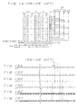
- Figs. 15A through 15F illustrate an exemplary timing chart of the transfer clocks in the inline transfer CCD given in Fig. 14 (prior art).
- the accumulated charges read out into the vertical transfer section 101 from the photosensitive section 100 are transferred in a vertical direction (in a direction of a downward-pointing arrow in Fig. 14) to be timed to the vertical transfer clocks ⁇ V1, ⁇ V2, ⁇ V3 and ⁇ V4 at a starting point of a signal transmission period 6.
- the accumulated charges at a bottom end of the vertical transfer section 101 are vertically transferred to the horizontal transfer section 102.
- the accumulated charges in the horizontal transfer section 102 are transferred in a horizontal direction (in a direction of a leftward-pointing arrow in Fig. 14), and then outputted as a picked-up image signal to an external CDS circuit (not shown).
- This CDS circuit thereafter performs sampling on the signal of the received accumulated charges.
- Fig. 16 is a block diagram illustrating the configuration of an imaging device introduced in Japanese Patent Application Laid-Open No. 2000-224473.
- incident light passing through a lens 105 is converted into a video signal by a CCD 106.
- the video signal is then sampled by a CDS circuit 107 and inputted to a low-intensity light detecting circuit 115.
- the low-intensity light detecting circuit 115 outputs a low-intensity light signal.
- An ALC circuit 114 controls an aperture of the lens 105.
- the video signal is converted into a digital video signal by an A/D converting circuit 109.
- a signal combining circuit 110 combines three or more digital video signals corresponding to adjacent pixels, and thereafter, performs division in such a manner that a resultant gain is more than 1.
- the signal combining circuit 110 outputs the result therein in response to the control by a gain-up control circuit 116.
- a signal processing circuit 111 performs predetermined signal processing on the video signal. After passing through a D/A converting circuit 112, the video signal is then outputted from an encoding circuit 113.
- the conventional imaging device has a signal processing circuit using a signal combining circuit for combining adjacent pixels and a divider circuit.
- the conventional imaging device has a problem involving reduction in S/N ratio on a displayed image obtained by a shooting under low-intensity light conditions.
- the conventional imaging device performs gain-up control of a digital signal obtained after A/D conversion, thus resulting in a problem of loss of bit information.
- a first aspect of the present invention is intended for an imaging device including an imaging element, a picked-up image signal processor, an imaging system controller, and a timing generator.
- the imaging element accumulates charges obtained by photoelectric conversion of incident light providing an image of a subject, transmits accumulated charges to an output terminal in response to a vertical transfer clock and a horizontal transfer clock, and outputs the accumulated charges from the output terminal.
- the picked-up image signal processor has an input terminal connected to the output terminal of the imaging element, and an output terminal.
- the picked-up image signal processor performs predetermined signal processings on the accumulated charges received at the input terminal thereof, and outputs a resultant signal as a picked-up image signal from the output terminal thereof.
- the imaging system controller has an output terminal.
- the imaging system controller outputs a control signal from the output terminal thereof.
- the control signal gives a command to generate and output the vertical transfer clock and the horizontal transfer clock in a signal transmission period, a command to suspend output of the vertical transfer clock an the horizontal transfer clock in an idle period subsequent to the signal transmission period, and a command to periodically repeat the signal transmission period and the idle period a number of times corresponding to the number of horizontal lines of the imaging element.
- the timing generator has an input terminal connected to the output terminal of the imaging system controller, and an output terminal connected to the imaging element. The timing generator generates and outputs the vertical transfer clock and the horizontal transfer clock from the output terminal thereof in the signal transmission period, and suspends output of the vertical transfer clock and the horizontal transfer clock in the idle period in response to the control signal received at the input terminal thereof.
- the length of the idle period is n times (n is a natural number) the length of the signal transmission period.
- the present invention employs an intermittent driving system capable of controlling a frame period to have a long length.
- the imaging element is allowed to accumulate charges spending frame time period of a length that is at least twice the length in the normal driving system. As a result, signal amplification by an amplifier is not required, thus leading to improvement in S/N ratio.
- a second aspect of the present invention is intended for an imaging device including an imaging element, a picked-up signal processor, an imaging system controller, a timing generator, and a signal level detector.
- the imaging element accumulates charges obtained by photoelectric conversion of incident light providing an image of a subject, transmits accumulated charges to an output terminal in response to a vertical transfer clock and a horizontal transfer clock, and outputs the accumulated charges from the output terminal.
- the picked-up image signal processor has an input terminal connected to the output terminal of the imaging element, and first and second output terminals. The picked-up image signal processor performs predetermined signal processings on the accumulated charges received at the input terminal thereof, and outputs a resultant signal as a picked-up image signal from the first output terminal thereof.
- the picked-up image signal processor further outputs a signal from the second output terminal thereof.
- This signal is obtained in the course of the predetermined signal processings, and required for determining brightness level of the subject.
- the imaging system controller has an input terminal and an output terminal.
- the imaging system controller has an input terminal and an output terminal.
- the imaging system controller outputs a control signal from the output terminal thereof.
- the control signal gives a command to generate and output the vertical transfer clock and the horizontal transfer clock in a signal transmission period, a command to suspend output of the vertical transfer clock and the horizontal transfer clock in an idle period subsequent to the signal transmission period, and a command to periodically repeat the signal transmission period and the idle period as a number of times corresponding to the number of horizontal lines of the imaging element.
- the timing generator has an input terminal connected to the output terminal of the imaging system controller, and an output terminal connected to the imaging element.
- the timing generator generates and outputs the vertical transfer clock and the horizontal transfer clock from the output terminal thereof in the signal transmission period, and suspends output of the vertical transfer clock and the horizontal transfer clock in the idle period in response to the control signal received at the input terminal thereof.
- the signal level detector has an input terminal connected to the second output terminal of the picked-up image signal processor, and an output terminal connected to the input terminal of the imaging system controller.
- the signal level detector detects the brightness level of the subject on the basis of the signal received at the input terminal thereof, and outputs a result of detection from the output terminal thereof.
- the length of the idle period is n times (n is an integer of 0 or more) the length of the signal transmission period.
- the imaging system controller controls the length of the idle period on the basis of the result of detection received at the input terminal thereof.
- a time period for accumulating charges in the imaging element can be thus controlled. More particularly, this time period is extended in a shooting under low-intensity light conditions, and is shortened under high-intensity light conditions.
- a third aspect of the present invention is intended for an imaging device including an imaging element, picked-up signal processing means, imaging system control means, and timing generating means.
- the imaging element accumulates charges obtained by photoelectric conversion of incident light providing an image of a subject, transmits accumulated charges to an output terminal in response to a vertical transfer clock and a horizontal transfer clock, and outputs the accumulated charges from the output terminal.
- the picked-up image signal processing means has an input terminal connected to the output terminal of the imaging element, and an output terminal.
- the picked-up image signal processing means performs predetermined signal processings on the accumulated charges received at the input terminal thereof, and outputs a resultant signal as a picked-up image signal from the output terminal thereof.
- the imaging system control means has an output terminal.
- the imaging system control means outputs a control signal from the output terminal thereof.
- the control signal gives a command to generate and output the vertical transfer clock and the horizontal transfer clock in a signal transmission period, a command to suspend output of the vertical transfer clock and the horizontal transfer clock in an idle period subsequent to the signal transmission period, and a command to periodically repeat the signal transmission period and the idle period a number of times corresponding to the number of horizontal lines of the imaging element.
- the timing generating means has an input terminal connected to the output terminal of the imaging system control means, and an output terminal connected to the imaging element.
- the timing generating means generates and outputs the vertical transfer clock and the horizontal transfer clock from the output terminal thereof in the signal transmission period, and suspends output of the vertical transfer clock and the horizontal transfer clock in the idle period in response to the control signal received at the input terminal thereof.
- the length of the idle period is n times (n is a natural number) the length of the signal transmission period.
- the present invention employs an intermittent driving system capable of controlling a frame period to have a long period of time.
- the imaging element is allowed to accumulate charges spending time of a length that is at least twice the length in the normal driving system. As a result, signal amplification by an amplifier is not required, thus leading to improvement in S/N ratio.
- an intermittent driving method of a solid state imaging element such as a CCD is suggested.
- This intermittent driving method requires the following: (1) in a signal transmission period, charges accumulated in all the pixels belonging to one horizontal line of the imaging element are transferred to an output terminal of the imaging element; (2) in an idle period (having a length that is a multiple of the length of the signal transmission period by a natural number) subsequent to the signal transmission period, no transfer of accumulated charges belonging to the next horizontal line is to occur; and (3) the signal transmission period and idle period are periodically repeated a number of times corresponding to the number of horizontal lines of the imaging element.
- Fig. 1 is a block diagram illustrating the system configuration of an imaging device 10 according to the first preferred embodiment.
- an imaging element 1 performs photoelectric conversion of incident light for providing a subject image, and accumulates charges obtained after conversion in corresponding pixels of each horizontal line.
- the imaging element 1 also sequentially transfers the charges accumulated in each of the pixels belonging to one horizontal line to an output terminal thereof, and thereafter outputs the accumulated charges from the output terminal.
- the exemplary structure of the imaging element 1 is shown in Fig. 2.
- the structure given in Fig. 2 is the same as given in Fig. 14 as discussed above.
- the photosensitive section 100 is corresponding to a plurality of pixels arranged along one horizontal line.
- the photosensitive section 100 includes four pixels for performing photosensitive conversion of incident light.
- the vertical transfer section 101 reads charges accumulated in each pixel belonging to the corresponding horizontal line, and sequentially transfer the accumulated charges to the horizontal transfer section 102 in a vertical direction (in a direction of a downward-pointing arrow in Fig. 2) (vertical transfer).
- the horizontal transfer section 102 receives the accumulated charges sequentially transferred thereto, and transfers the same to the output terminal in response to the timing of the horizontal transfer clocks ⁇ H1 and ⁇ H2 (horizontal transfer).
- a timing generator 2 has an input terminal connected to a first output terminal of a to-be-described imaging system controller 5, and an output terminal connected to an input terminal of the imaging element 1.
- the timing generator 2 supplies the vertical transfer clock ⁇ Vn and the horizontal transfer clock ⁇ Hm to the vertical transfer section 101 and to the horizontal transfer section 102 of the imaging element 1, respectively.
- a picked-up image signal processor 3 has a first input terminal connected to the output terminal of the imaging element 1, a second input terminal connected to a second output terminal of the imaging system controller 5, a data writing and reading terminal, and an output terminal.
- the picked-up image signal processor 3 receives accumulated charges V1 outputted from the imaging element 1, and performs predetermined signal processings on the signal V1.
- the configuration of the picked-up image signal processor 3 is shown in Fig. 3. As seen from Fig.
- the picked-up image signal processor 3 includes a CDS circuit 15 for performing a signal processing (sampling) on the accumulated charges V1 received from the imaging element 1, an AGC circuit 16 for amplifying the signal received from the CDS circuit 15, an A/D converting circuit 17 for converting the output from the AGC circuit 16 into a digital signal, and a signal processing circuit 18 for processing the output from the A/D converting circuit 17 into a signal of a format optimally suitable for a camera.
- a line memory 4 is connected to the data writing and reading terminal of the picked-up image signal processor 3. To be timed to a writing and reading clock signal VCC, the line memory 4 temporarily stores a picked-up image signal (digital signal) V2, that is obtained from the foregoing predetermined signal processings, for each line.
- the imaging system controller 5 is a core section of the imaging device 10 which manages schedules such as a readout time period of the accumulated charges in a direction of each horizontal line of the imaging element 1 and the number of horizontal lines of the imaging element 1, and includes a counter (not shown) therein.
- the imaging system controller 5 controls generation and output of the vertical transfer clock ⁇ Vn and the horizontal transfer clock ⁇ Hm at the timing generator 2, and writing and reading of the picked-up image signal V2 by the picked-up image signal processor 3 to and from the line memory 4.
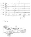
- Figs. 4A through 4F illustrating a timing chart of the transfer clocks ⁇ Vn (n is an integer ranging from 1 to 4) and ⁇ Hm (m indicates either 1 or 2) outputted from the timing generator 2.
- the imaging system controller 5 controls generation and output of the transfer clocks ⁇ Vn and ⁇ Hm at the timing generator 2.
- reference numeral 6 denotes a signal transmission period for transmitting data belonging to one horizontal line
- numeral 7 denotes an idle period in which no transmission of data belonging to k horizontal lines (k is a natural number) occurs.
- the idle period 7 is a period in which no transmission of data belonging to three horizontal lines occurs.
- the ratio in length between the periods 6 and 7 is determined by the imaging system controller 5.
- the imaging system controller 5 is operable (1) to predetermine the lengths of the signal transmission period 6 and the idle period 7 on the basis of the readout time period of all the accumulated charges V1 belonging to one horizontal line of the imaging element 1, and then, (2) to generate the control signal VC giving the following commands in response to the time counted by the counter therein, and output the control signal VC from its output terminal to the timing generator 2.
- the commands given from the control signal VC includes (i) a command to generate and output the vertical transfer clock ⁇ Vn and the horizontal transfer clock ⁇ Hm in the signal transmission period 6, (ii) a command to suspend output of both the vertical transfer clock ⁇ Vn and the horizontal transfer clock ⁇ Hm in the idle period 7 subsequent to the signal transmission period 6, and (iii) a command to periodically repeat a frame period 8 including the signal transmission period 6 and the idle period 7 (see Fig. 6) a number of times corresponding to the number of horizontal lines of the imaging element 1.
- the length of the idle period 7 is k times (k is a natural number) the length of the signal transmission period 6.
- the timing generator 2 In response to the commands of the control signal VC, the timing generator 2 generates and outputs the vertical transfer clock ⁇ Vn and the horizontal transfer clock ⁇ Hm from its output terminal in the signal transmission period 6, and suspends output of the vertical transfer clock ⁇ Vn and the horizontal transfer clock ⁇ Hm in the idle period 7. The timing generator 2 periodically repeats these operations in response to the commands of the control signal VC.
- the imaging system controller 5 controls the timing generator 2 so as to transmit the transfer clocks ⁇ V1 through ⁇ V4, ⁇ H1 and ⁇ H2 to the input terminal of the imaging element 1 in the signal transmission period 6.
- the timing generator 2 Upon receipt of this control by the imaging system controller 5, the timing generator 2 outputs the transfer clocks ⁇ V1 through ⁇ V4, ⁇ H1 and ⁇ H2 to drive the imaging element 1.
- the accumulated charges V1 are thus read out from the imaging element 1 and transmitted to the picked-up image signal processor 3, at which the signal V1 undergo predetermined signal processings. As a result, the picked-up image signal V2 is obtained.
- the imaging system controller 5 controls the timing generator 2 so as to suspend output of the transfer clocks ⁇ V1 through ⁇ V4, ⁇ H1 and ⁇ H2.
- the timing generator 2 thus suspends output of the transfer clocks ⁇ V1 through ⁇ V4, ⁇ H1 and ⁇ H2 in this period.
- the imaging system controller 5 continues to control the timing generator 2 so as to suspend output of the transfer clocks ⁇ V1 through ⁇ V4, ⁇ H1 and ⁇ H2.
- the timing generator 2 thus continues to suspend output of the transfer clocks ⁇ V1 through ⁇ V4, ⁇ H1 and ⁇ H2 in this period corresponding to these two horizontal lines.
- the imaging system controller 5 periodically repeats such control of the signal transmission period 6 and the idle period 7 a number of times corresponding to the number of horizontal lines of the imaging element 1, namely, performs "intermittent driving". According to this intermittent driving method, all the accumulated charges corresponding to one screen of the picked-up image can be read out.
- the intermittent driving method shown in Figs. 4A through 4F produces the following effect. That is, in each transmission period, namely, in each idle period 7, charge accumulation simultaneously occurs in all the pixels of the photosensitive section 100 of the imaging element 1. Charges are thereby accumulated spending a period of a length that is four times (generally speaking, (k+1) times) the length of a frame time period in the normal driving method requiring only the signal transmission period as shown in Fig. 15.
- signal amplification by an amplifier is not required, thus leading to improvement in S/N ratio.
- degradation of S/N ratio on a displayed image is prevented.
- the signal transmission period 6 corresponds to a period of one horizontal line and the idle period 7 corresponds to a period of three horizontal lines.
- the idle period 7 is required to have at least the same length as that of the signal transmission period 6. In this case, the foregoing effect is also achieved.
- the imaging system controller 5 generates the "writing and reading clock signal VCC" giving commands to temporarily store the picked-up image signal V2 in the line memory 4 in the signal transmission period 6, and to start reading of the picked-up image signal V2 from the line memory 4 to be timed to an arbitrary instant in the frame period 8 (corresponding to the sum of the signal transmission period 6 and the idle period 7; see Figs. 6A and 6B) and to finish this reading of the picked-up image signal V2 in the frame period 8.
- the imaging system controller 5 outputs the writing and reading clock signal VCC from its second output terminal to the picked-up image signal processor 3.
- the picked-up image signal processor 3 (more particularly, the signal processing circuit 18 in Fig. 3) thereby performs writing and reading of the picked-up image signal V2 to and from the line memory 4.
- the data V2 temporarily stored in the line memory 4 within the signal transmission period 6 can be taken out to be timed to an arbitrary instant by the end of the idle period 7 in the frame period 8 including this signal transmission period 6. As a result, timing for reading the picked-up image signal V2 can be easily determined.
- the imaging device 10 requires only the adjustment between the timing for reading the data from the line memory 4 and the timing for reading the charges from the imaging element 1, eliminating the necessity to provide a field memory having a capacity corresponding to the number of all the pixels of the imaging element 1. In view of this, the imaging device 10 is also advantageously applicable in terms of cost, mounting area and weight.
- Figs. 5A and 5B illustrate a timing chart showing waveforms of a writing clock signal Ckwh and a reading clock signal Ckrh provided for the line memory 4 in relation to a period tw of the writing clock signal Ckwh.
- Figs. 6A through 6C illustrate a timing chart showing timing of a writing clock signal Ckwf and reading clock signals Ckr1f, Ckr2f in relation to the frame period 8.
- the writing clock signal Ckwh (Ckwf) and the reading clock signal Ckrh (Ckrlf, Ckr2f) are collectively referred to as the writing and reading clock signal VCC.
- the writing clock signal Ckwh shown in Fig. 5A has a frequency (1/tw).
- n is an integer of not less than 1.
- Fig. 5B n is defined as 4.
- the waveform of the writing clock signal Ckwf shown in Fig. 6A corresponds to the waveform of the writing clock signal Ckwh in Fig. 5A when viewed with the frame period 8.
- the output period of the writing clock signal Ckwf is the same as the signal transmission period 6.
- n 1, namely, when the reading clock signal Ckrh is in synchronization with the writing clock signal Ckwh and has the same period as that of the writing clock signal Ckwh
- the waveform of the reading clock signal Ckr1f shown in Fig. 6B is obtained by controlling the phase of the reading clock signal Ckrh in Fig. 5B.
- the waveform of the reading clock signal Ckr1f is obtained by delaying the reading clock signal Ckrh relative to the writing clock signal Ckwh by a period of time longer than the signal transmission period 6. Further, the waveform of the reading clock signal Ckr1f is viewed with the frame period 8.
- the reading clock signal may be the signal Ckr2f in Fig. 6C. Under the condition of n >> 1, the waveform of the reading clock signal Ckr2f is obtained by controlling the phase of the reading clock signal Ckrh in Fig. 5B.
- the waveform of the reading clock signal Ckr2f is obtained by delaying the reading clock signal Ckrh relative to the writing clock signal Ckwh by a period of time corresponding to the signal transmission period 6. Further, the waveform of the reading clock signal Ckr2f is viewed with the frame period 8.
- the phase may be controlled to such an extent that timing for starting an output period of the reading clock signal viewed with the frame period 8 is shifted to the idle period 7.
- the phase may be controlled with clock period within the signal transmission period 6.
- the writing clock signal and the reading clock signal for the line memory 4 may be asynchronous to each other.
- the same horizontal clock ⁇ Hm is applicable as a driving clock (clock for reading accumulated charges) of the imaging element 1 to be outputted only in the signal transmission period 6.
- the adjustment of a black sample-and-hold pulse signal, a signal sample-and-hold pulse signal, an A/D clock signal and the like, which are supplied to the CDS circuit 15 and the A/D converting circuit 17 of the picked-up image signal processor 3, is not required for each frame period at all.
- the imaging device 10 does not require a memory therein having an adjusted value for each arbitrary frame period.
- the black sample-and-hold pulse signal and the signal sample-and-hold pulse signal can be shared in the picked-up image signal processor 3, thus fixing the relation in phase between these pulses and the horizontal transfer clock ⁇ Hm and eventually, preventing degradation of S/N ratio.
- the modification of the first preferred embodiment characteristically requires the following: (1) in a dummy transmission period 12 (see Fig. 7A), the imaging system controller 5 outputs the control signal VC which further commands to generate and output only the horizontal transfer clock ⁇ Hm; and (2) in response to the command of this control signal VC received in the dummy transmission period 12, the timing generator 2 generates and outputs only the horizontal clock signal ⁇ Hm in the dummy transmission period 12.
- the dummy transmission period 12 is provided in the idle period 7 and immediately before the signal transmission period 6 following this idle period 7.
- Figs. 7A through 7F illustrate a timing chart showing the waveform of each transfer clock when the imaging system controller 5 generates and outputs the control signal VC which commands to generate and output only the horizontal transfer clock ⁇ Hm in the dummy transmission period 12.
- the dummy transmission period 12 is a period provided in the idle period 7 immediately before a certain signal transmission period 6, ending immediately before this signal transmission period 6.
- the timing generator 2 suspends output of the vertical transfer clocks ⁇ V1 through ⁇ V4, and outputs only the horizontal transfer clocks ⁇ H1 and ⁇ H2 to drive only the horizontal transfer section 102 in the dummy transmission period 12.
- noise such as dark current accumulated in the horizontal transfer section 102 can be horizontally transferred, thus eliminating charges caused by residual current noise. It is therefore allowed to effectively transfer only the accumulated charges in the signal transmission period 6 subsequent to the dummy transmission period 12. As a result, accumulated charges can be transferred with higher S/N ratio.
- the second preferred embodiment of the present invention is the improvement of the first preferred embodiment, characteristically requiring the following. That is, a signal obtained in one of a plurality of signal processings in the picked-up image signal processor 3 or the picked-up image signal V2 which is a digital signal is detected, and then the ratio in length between the signal transmission period and the idle period is controlled according to the level of the detected signal, namely, to the brightness level of a subject image.
- Fig. 8 is a block diagram illustrating the system configuration of an imaging device 10A according to the second preferred embodiment.
- the distinctive features of the imaging device 10A from the imaging device 10 shown in Fig. 1 lie in the picked-up signal processor 3, a signal level detector 13 and the imaging system controller 5.
- the description in the first preferred embodiment is to be further applied in the second preferred embodiment.
- the picked-up image signal processor 3 has a first input terminal connected to the output terminal of the imaging element 1, a second input terminal for receiving the writing and reading clock signal VCC, a first output terminal for outputting the picked-up image signal V2, and a second output terminal. More particularly, the picked-up image signal processor 3 outputs a signal V2A, which is obtained in the course of predetermined signal processings on the accumulated charges V1, from its second output terminal.
- the signal VIA is used to determine brightness level of the subject image.
- the signal level detector 13 has an input terminal connected to the second output terminal of the picked-up image signal processor 3, and an output terminal connected to the input terminal of the imaging system controller 5. More particularly, on receipt of the signal VIA received at the input terminal, the signal level detector 13 detects brightness level of the subject image, and outputs a result of detection V13 from the output terminal.
- the signal level detector 13 detects the level of the signal VIA outputted from the picked-up image signal processor 3.
- the imaging system controller 5 sets the idle period 7 to have a length shorter than its current length in response to this brightness level. A frame frequency is thus increased, leading to the shortened period of the frame period 8. Charges are thereby accumulated in the imaging element 1 within a shorter period of time. As a result, saturation of charges can be suppressed.
- the imaging system controller 5 controls the foregoing ratio so that the idle period 7 should be always provided (when the method shifts from the normal driving to the intermittent driving), or alternatively, the idle period 7 has a length longer than the current one (when the imaging element 1 has been already driven by the intermittent method). A frame frequency is thus decreased and charges are accumulated in the imaging element 1 spending a longer period of time. As a result, the amount of accumulated charges can be increased.
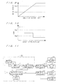
- Fig. 9 shows the signal output from the CDS circuit 15. As the amount of light incident on the imaging element 1 increases, the output data from the CDS circuit 15 continues to increase until it reaches a saturation level from the point of the certain amount of incident light onward. The characteristic shown in Fig. 9 differs depending on the system configuration.
- the signal level detector 13 has two threshold values ths1 and ths0 with respect to the output signal from the CDS circuit 15.
- the state where the output signal from the CDS circuit 15 ranges between the threshold values ths1 and ths0 is defined as a standard state for adjusting the idle period 7.
- the imaging system controller 5 sets the ratio in length between the signal transmission period 6 and the idle period 7 to be 1:1.
- the signal level detector 13 determines that the subject image has a higher brightness level than the one obtained in the standard state.
- the imaging system controller 5 sets the ratio in length between the signal transmission period 6 and the idle period 7 to be 1:0. Namely, the imaging system controller 5 outputs a signal VCA, which commands to stop the intermittent driving to thereafter shift to the normal driving, to the timing generator 2.
- the signal level detector 13 determines that the subject image is in shooting conditions of lower brightness level.
- the imaging system controller 5 sets the ratio in length between the signal transmission period 6 and the idle period 7 to be 1:3. By extending the idle period 7 in this manner, the imaging system controller 5 or the timing generator 2 extends the exposure time in the imaging element 1, to increase the amount of accumulated charges.
- the length of the idle period 7 is adjusted or controlled in three levels according to the output level from the CDS circuit 15.
- the ratio in length between the signal transmission period 6 and the idle period 7 can be controlled on the basis of the brightness level of the subject image. In other words, according to the conditions of the subject during shooting, the length of the idle period 7 can be optimally adjusted.
- the brightness level may be determined using the signal for providing the amount of gain of the AGC circuit 16 in Fig. 3 as the signal V2A.
- Fig. 10 shows the exemplary gain characteristic of the AGC circuit 16. The characteristic shown therein differs depending on the system configuration.
- the gain characteristic of the AGC circuit 16 is varied in three levels according to the amount of incident light.
- the signal level detector 13 is shown to have two threshold values thg1 and thg0 with respect to the above-mentioned gain characteristic.
- the state where the gain of the AGC circuit 16 ranges between the threshold values thg1 and thg0 is defined as a standard state for adjusting the length of the idle period 7.
- the imaging system controller 5 changes the ratio in length between the signal transmission period 6 and the idle period 7 as determined in the normal state.
- the length of the idle period 7 can be also suitably adjusted in three levels according to the conditions of the subject during shooting.
- the signal level detector 13 is shown to have two threshold values respectively. However, the second preferred embodiment is still applicable even with the arbitrary number of these threshold values.
- the picked-up image signal V2 itself outputted from the signal processing circuit 18 can be used as the signal V2A.
- the first and second output terminals of the picked-up image signal processor 3 are the same.
- the exemplary system configuration of the imaging device employing an intermittent driving method has been discussed. According to this intermittent driving method, charges accumulated in the imaging element are transferred in the signal transmission period and in the subsequent idle period, transfer of the accumulated charges is suspended.
- the imaging device according to the first preferred embodiment (including the modification thereof) or to the second preferred embodiment is applied to a portable terminal such as a mobile computer.
- a portable terminal equipped with the imaging device 10 according to the first preferred embodiment will be discussed below.
- Fig. 11 is a block diagram illustrating the system configuration of the portable terminal device including the imaging device 10 given in Fig. 1.
- a main system controller 19 is a core section for performing the schedule administration for the portable terminal device.
- a main signal processor 20 performs predetermined signal processings on the picked-up image signal V2 transmitted from the picked-up image signal processor 3.
- the signal processings in the main signal processor 20 include (1) in a monitor mode, a processing for converting the picked-up image signal V2 into a monitor moving picture signal (display data) suitably applicable for display on a to-be-described display device 21, and (2) in a record mode, a processing for converting the picked-up image signal V2 into a record signal suitably applicable for recording on a to-be-described recording device 22.
- the display device 21 is a flat panel display (FPD) which may be a liquid crystal display (LCD), or alternatively, an organic or inorganic EL display.
- FPD flat panel display
- LCD liquid crystal display
- OLED organic or inorganic EL display
- the recording device 22 records the record signal outputted from the main signal processor 20 on a memory element such as a flash memory.
- an image capturing switch 23 outputs an imaging command signal to the main system controller 19.
- a setting switch 24 is operable to determine the number of pixels to be stored in the recording device 22, to determine whether the imaging device 10 should be brought to an operating state, and to control the state of the portable terminal device.
- the main system controller 19 When the image capturing switch 23 of the portable terminal device is pressed, the main system controller 19 outputs the imaging command signal which commands or demands to start imaging of the subject into the imaging system controller 5. On receipt of this signal outputted from the main system controller 19, the imaging system controller 5 executes imaging according to the foregoing intermittent driving. After completion of the imaging, the imaging system controller 5 issues a demand to the main system controller 19 in order to start data transmission of the picked-up image signal V2. On receipt of this demand, the main system controller 19 determines whether or not the main signal processor 20 is in a state allowing receipt of the picked-up image signal data.
- the main system controller 19 transmits a data transmission command signal, which commands to start transmission of the picked-up image signal V2, to the imaging system controller 5.
- the imaging system controller 5 controls reading of the picked-up image signal data by the picked-up image signal processor 3.
- the main signal processor 20 receives the picked-up image signal V2 outputted and transmitted from the picked-up image signal processor 3.
- the imaging system controller 5 sets and maintains the length of the idle period 7 to be the same as that of the data transmission period of the picked-up image signal V2.
- the data transmission of the picked-up image signal V2 can be thus handled only by the line memory 4, requiring no frame memory having a memory capacity corresponding to all the pixels of the imaging element 1.
- the user selects the subject and determines the angle of view of the subject, for example.
- the imaging system controller 5 controls the system to shift to the normal driving having no idle period.
- the frame frequency is increased accordingly, namely, the length of the frame period is shortened.
- the resolution of the data transmitted from the picked-up image signal processor 3 is thereby lowered enough to allow a monitor image to be displayed on the display device 21.
- the portable terminal device realizes monitor mode allowing the subject to be monitored as a moving image.
- the imaging device 10 When the image capturing switch 23 is pressed, on the other hand, the imaging device 10 is placed under conditions in which shooting of the subject is executed. The imaging system controller 5 then controls the system to shift to the intermittent driving as described. The frame frequency is decreased accordingly to such a degree that the picked-up image signal V2 has a desirable resolution for recording, and thereafter, the picked-up image signal V2 having such resolution is transmitted. As a result, the portable terminal device according to the third preferred embodiment realizes recording mode of data.
- the imaging system controller 5 executing the foregoing control (namely, shift between normal driving and intermittent driving), the picked-up image signal data which is optimally controlled for both the monitor mode and the record mode can be transmitted.
- the display device 21 allows high-quality display.
- Fig. 12 is a flowchart showing the sequence of the operations of the portable terminal device according to the third preferred embodiment, namely, the operations determining the states in the monitor mode and the record mode, and then shifting the driving method between normal driving (with no idle period) and intermittent driving (with idle period).
- the imaging system controller 5 is in the state of waiting a demand to start imaging (step S1). At this time, the imaging system controller 5 outputs the control signal VC, which commands to control the transfer of accumulated charges in the image element 1 by the normal driving method, to the timing generator 2.
- the picked-up image signal processor 3 thereby performs the signal processings on the accumulated charges V1 transmitted by the normal driving method, and outputs the resultant picked-up image signal V2 to the main signal processor 20.
- the system is placed in the monitor mode in which a moving picture having an exemplary frame rate of 20 fps is displayed on the display device 21 of an exemplary size including 160 ⁇ 120 pixels.
- the main system controller 19 issues a demand to start imaging.
- the imaging system controller 5 outputs the control signal VC, which commands so as to transfer accumulated charges in the imaging element 1 by the intermittent driving method, to the timing generator 2.
- the picked-up image signal processor 3 thereby performs the above-mentioned signal processings on the accumulated charges V1 intermittently transmitted thereto, and outputs the resultant picked-up image signal V2 to the main signal processor 20 (step S2).
- the frame rate is reduced to a value that is one-sixteenth the value of the frame rate of 20 fps in the monitor mode, namely, about 1 fps. Data transmission of the picked-up image signal V2 is thereby allowed.
- the main signal processor 20 performs a signal processing on the received picked-up image signal V2 for converting the same into record data, and records the obtained data on the recording device 22.
- the steps S2 through S4 are repeatedly performed until imaging is completed.
- the operations described so far while maintaining display quality, it is allowed to display a moving picture in the monitor mode and transmit data having a large number of pixels (still picture) in the record mode.
- the moving picture data of low resolution displayed in the monitor mode may be recorded in the record mode.
- the third preferred embodiment produces the following result (1). That is, transmission of the picked-up image signal can be handled only by the line memory without the necessity of providing a frame memory having a capacity corresponding to all the pixels of the imaging element.
- the third preferred embodiment further produces the following result (2). That is, in the monitor mode, a moving picture having a resolution suitable for this mode can be displayed, and in the record mode, data can be recorded with a desirable resolution.
- FIG. 17 The exemplary configuration of the third preferred embodiment equipped with the imaging device 10A according to the second preferred embodiment (Fig. 8) is illustrated in Fig. 17.
- the fundamental operations of this system are the same as those described so far.
- the fourth preferred embodiment of the present invention relates to a portable terminal including wireless communications (such as portable phone, PDA, or portable television) equipped with the imaging device according to the first preferred embodiment (including the modification thereof) or to the second preferred embodiment.
- wireless communications such as portable phone, PDA, or portable television
- the first preferred embodiment is applied for the sake of convenience to the portable terminal including wireless communications.
- Fig. 13 is a block diagram illustrating the exemplary configuration of the system employing the portable phone including wireless communications.
- the communication processor 25 is connected to the main signal processor 20 through the main system controller 19.
- the communication processor 25 transmits the picked-up image data of the subject received from the main signal processor 20 into the external storage device 26 through wireless communications.
- the external storage device 26 stores the data of the picked-up image transmitted thereto through communications with the portable phone.
- the system may be configured without the external storage device 26.
- a fundamental frequency of a system clock may vary by the influence such as condition of reception.
- a system clock in the main system controller 19 can be also employed as the driving clocks, or as the transfer clocks ⁇ Vn and ⁇ Hm of the imaging element 1.
- the imaging device 10 does not require a plurality of oscillators and PLL circuits therein for generating the transfer clocks ⁇ Vn and ⁇ Hm of the imaging element 1, thus readily realizing the portable phone equipped with the imaging device 10.
- the length of the idle period 7 is determined in response to the transmission speed of the foregoing data of the picked-up image from the communication processor 25 to the external storage device 26. More particularly, when the speed at which data is transmitted from the communication processor 25 to the external storage device 26 is lower than the speed at which data is transmitted from the picked-up image signal processor 3 to the main signal processor 20, the imaging system controller 5 sets the length of the idle period 7 to be suitably applicable for the data transmission speed between the communication processor 25 and the external storage device 26, and then controls the timing generator 2 to induce transmission of the accumulated charges V1 from the imaging element 1 by the intermittent driving method. According to the configuration described so far, without the necessity of providing a mass storage region in the portable phone, the data of the picked-up image obtained from the picked-up image signal V2 can be reliably transmitted to and recorded on the external storage device 26.
- FIG. 18 The exemplary configuration of the fourth preferred embodiment equipped with the imaging device 10A according to the second preferred embodiment (Fig. 8) is shown in Fig. 18.
- the fundamental operations, functions and effects are the same as those described so far.
Landscapes
- Engineering & Computer Science (AREA)
- Multimedia (AREA)
- Signal Processing (AREA)
- Transforming Light Signals Into Electric Signals (AREA)
- Studio Devices (AREA)
- Solid State Image Pick-Up Elements (AREA)
- Telephone Set Structure (AREA)
- Mobile Radio Communication Systems (AREA)
Abstract
Description
Claims (12)
- An imaging device, comprising:an imaging element <1> for accumulating charges obtained by photoelectric conversion of incident light providing an image of a subject, said imaging element transmitting accumulated charges <V1> to an output terminal in response to a vertical transfer clock <Vn> and a horizontal transfer clock <Hm>, and outputting said accumulated charges from said output terminal;a picked-up image signal processor <3> having an input terminal connected to said output terminal of said imaging element, and an output terminal, said picked-up image signal processor performing predetermined signal processings on said accumulated charges received at said input terminal thereof, and outputting a resultant signal as a picked-up image signal <V2> from said output terminal thereof;an imaging system controller <5> having an output terminal, said imaging system controller outputting a control signal <VC> from said output terminal thereof, said control signal giving a command to generate and output said vertical transfer clock and said horizontal transfer clock in a signal transmission period <6>, a command to suspend output of said vertical transfer clock and said horizontal transfer clock in an idle period <7> subsequent to said signal transmission period, and a command to periodically repeat said signal transmission period and said idle period a number of times corresponding to the number of horizontal lines of said imaging element; anda timing generator <2> having an input terminal connected to said output terminal of said imaging system controller, and an output terminal connected to said imaging element, said timing generator generating and outputting said vertical transfer clock and said horizontal transfer clock from said output terminal thereof in said signal transmission period, and suspending output of said vertical transfer clock and said horizontal transfer clock in said idle period in response to said control signal received at said input terminal thereof, whereinthe length of said idle period <7> is n times (n is a natural number) the length of said signal transmission period <6>.
- The imaging device according to claim 1, wherein
said imaging system controller <5> further outputs a signal as said control signal <VC>, said control signal giving a command to generate and output only said horizontal transfer clock in a dummy period <12>,
said timing generator <2> generates only said horizontal transfer clock <Hm> in said dummy transfer period <12> in response to said control signal, and
said dummy transfer period <12> is provided in said idle period <7> and immediately before said signal transmission period <6> subsequent to said idle period <7>. - The imaging device according to claim 1 or 2, wherein
said imaging system controller <5> has said output terminal as a first output terminal, said imaging system controller further having a second output terminal,
said picked-up image signal processor <3> has said input terminal as a first input terminal, said picked-up image signal processor further having a second input terminal connected to said second output terminal of said imaging system controller, and a data writing and reading terminal,
said imaging device <10> further comprises a line memory <4> connected to said data writing and reading terminal of said picked-up image signal processor,
said imaging system controller <5> outputs a writing and reading clock signal <VCC> from said second output terminal thereof, said writing and reading clock signal giving a command to store said picked-up image signal <V2> in said line memory <4> in said signal transmission period <6>, and a command to start reading of said picked-up image signal from said line memory to be timed to an arbitrary instant in a frame period <8>, said writing and reading clock signal further giving a command to finish said reading of said picked-up image signal in said frame period <8>,
said picked-up image signal processor <3> performs writing and reading of said picked-up image signal to and from said line memory to be timed to said writing and reading clock signal <VCC>, and
said frame period <8> corresponds to a sum of said signal transmission period <6> and said idle period <7>. - A portable terminal, comprising:said imaging device <10> as recited in claim 3;a main system controller <19> for outputting an imaging command signal and a data transmission command signal to said imaging system controller, said imaging command signal giving a command to start imaging of said subject, and said data transmission command signal giving a command to start transmission of said picked-up image signal after completion of imaging of said subject; anda main signal processor <20> for receiving said picked-up image signal outputted from said picked-up image signal processor, and performing predetermined signal processings on said picked-up image signal, whereinsaid idle period <7> is controlled to have a length that is the same as a time period for transmitting said picked-up image signal to said main signal processor.
- The portable terminal according to claim 4, further comprising:a display device <21> connected to said main signal processor; anda recording device <22> connected to said main signal processor, whereinin a monitor mode where no output of said imaging command signal occurs from said main system controller to said imaging system controller, said imaging system controller <5> provides no idle period and controls imaging of said subject and transmission of said picked-up image signal by normal driving, andin a record mode where said imaging command signal is outputted from said main system controller to said imaging system controller, said imaging system controller <5> provides said idle period and controls imaging of said subject and transmission of said picked-up image signal by intermittent driving.
- The portable terminal according to claim 5, further comprising:a communication processor <25> connected to said main signal processor <20> through said main system controller <19>, said communication processor handling wireless communications with an external storage device <26>, said external storage device recording picked-up image data of said subject, whereinthe length of said idle period <7> is determined in response to a speed at which said picked-up image data is transmitted from said communication processor <25> to said external storage device <26>.
- An imaging device, comprising:an imaging element <1> for accumulating charges obtained by photoelectric conversion of incident light providing an image of a subject, said imaging element transmitting accumulated charges <V1> to an output terminal in response to a vertical transfer clock <Vn> and a horizontal transfer clock <Hm>, and outputting said accumulated charges from said output terminal;a picked-up image signal processor <3> having an input terminal connected to said output terminal of said imaging element, and first and second output terminals, said picked-up image signal processor performing predetermined signal processings on said accumulated charges received at said input terminal thereof, and outputting a resultant signal as a picked-up image signal <V2> from said first output terminal thereof, said picked-up image signal processor further outputting a signal <V2A> from said second output terminal thereof, said signal <V2A> being obtained in the course of said predetermined signal processings and required for determining brightness level of said subject;an imaging system controller <5> having an input terminal and an output terminal, said imaging system controller outputting a control signal <VCA> from said output terminal thereof, said control signal giving a command to generate and output said vertical transfer clock and said horizontal transfer clock in a signal transmission period, a command to suspend output of said vertical transfer clock and said horizontal transfer clock in an idle period subsequent to said signal transmission period, and a command to periodically repeat said signal transmission period and said idle period a number of times corresponding to the number of horizontal lines of said imaging element;a timing generator <2> having an input terminal connected to said output terminal of said imaging system controller, and an output terminal connected to said imaging element, said timing generator generating and outputting said vertical transfer clock and said horizontal transfer clock from said output terminal thereof in said signal transmission period, and suspending output of said vertical transfer clock and said horizontal transfer clock in said idle period in response to said control signal received at said input terminal thereof; anda signal level detector <13> having an input terminal connected to said second output terminal of said picked-up image signal processor, and an output terminal connected to said input terminal of said imaging system controller, said signal level detector detecting said brightness level of said subject on the basis of said signal <V2A> received at said input terminal thereof, and outputting a result of detection <V13> from said output terminal thereof, whereinthe length of said idle period <7> is n times (n is an integer of 0 or more) the length of said signal transmission period <6>, andsaid imaging system controller <5> controls the length of said idle period on the basis of said result of detection received at said input terminal thereof.
- The imaging device according to claim 7, wherein
said imaging system controller <5> has said output terminal as a first output terminal, said imaging system controller further having a second output terminal,
said picked-up image signal processor <3> has said input terminal as a first input terminal, said picked-up image signal processor further having a second input terminal connected to said second output terminal of said imaging system controller, and a data writing and reading terminal,
said imaging device <10A> further comprises a line memory <4> connected to said data writing and reading terminal of said picked-up image signal processor,
said imaging system controller <5> outputs a writing and reading clock signal <VCC> from said second output terminal thereof, said writing and reading clock signal giving a command to store said picked-up image signal in said line memory in said signal transmission period, and a command to start reading of said picked-up image signal from said line memory to be timed to an arbitrary instant in a frame period <8>, said writing and reading clock signal further giving a command to finish said reading of said picked-up image signal in said frame period,
said picked-up image signal processor <3> performs writing and reading of said picked-up image signal <V2> to and from said line memory <4> to be timed to said writing and reading clock signal <VCC>, and
said frame period <8> corresponds to a sum of said signal transmission period <6> and said idle period <7>. - A portable terminal, comprising:said imaging device <10A> as recited in claim 8;a main system controller <19> for outputting an imaging command signal and a data transmission command signal to said imaging system controller <5>, said imaging command signal giving a command to start imaging of said subject, and said data transmission command signal giving a command to start transmission of said picked-up image signal after completion of imaging of said subject; anda main signal processor <20> for receiving said picked-up image signal <V2> outputted from said picked-up image signal processor <3>, and performing predetermined signal processings on said picked-up image signal, whereinsaid idle period <7> is controlled to have a length that is the same as a time period for transmitting said picked-up image signal to said main signal processor.
- The portable terminal according to claim 9, further comprising:a display device <21> connected to said main signal processor; anda recording device <22> connected to said main signal processor, whereinin a monitor mode where no output of said imaging command signal occurs from said main system controller <19> to said imaging system controller, said imaging system controller <5> provides no idle period and controls imaging of said subject and transmission of said picked-up image signal by normal driving, andin a record mode where said imaging command signal is outputted from said main system controller <19> to said imaging system controller, said imaging system controller <5> provides said idle period and controls imaging of said subject and transmission of said picked-up image signal by intermittent driving.
- The portable terminal according to claim 10, further comprising:a communication processor <25> connected to said main signal processor <20> through said main system controller <19>, said communication processor handling wireless communications with an external storage device <26>, said external storage device recording picked-up image data of said subject, whereinthe length of said idle period <7> is determined in response to a speed at which said picked-up image data is transmitted from said communication processor <25> to said external storage device <26>.
- An image pick-up device comprising an imaging element for accumulating charges from photoelectric conversion of incident light, and means for adjusting the time period for accumulating charges according to the lighting conditions.
Applications Claiming Priority (2)
| Application Number | Priority Date | Filing Date | Title |
|---|---|---|---|
| JP2002103504A JP3964718B2 (en) | 2002-04-05 | 2002-04-05 | Imaging device and portable terminal |
| JP2002103504 | 2002-04-05 |
Publications (2)
| Publication Number | Publication Date |
|---|---|
| EP1351499A2 true EP1351499A2 (en) | 2003-10-08 |
| EP1351499A3 EP1351499A3 (en) | 2005-01-26 |
Family
ID=28035960
Family Applications (1)
| Application Number | Title | Priority Date | Filing Date |
|---|---|---|---|
| EP02256860A Withdrawn EP1351499A3 (en) | 2002-04-05 | 2002-10-02 | Imaging device and portable terminal |
Country Status (3)
| Country | Link |
|---|---|
| US (1) | US7324147B2 (en) |
| EP (1) | EP1351499A3 (en) |
| JP (1) | JP3964718B2 (en) |
Families Citing this family (9)
| Publication number | Priority date | Publication date | Assignee | Title |
|---|---|---|---|---|
| JP2004165912A (en) * | 2002-11-12 | 2004-06-10 | Canon Inc | Method and apparatus for driving area image sensor |
| US6845061B2 (en) * | 2003-02-05 | 2005-01-18 | Megawin Technology Co., Ltd. | Method for quickly detecting the state of a nonvolatile storage medium |
| JP2006352723A (en) * | 2005-06-20 | 2006-12-28 | Eastman Kodak Co | Imaging apparatus, imaging system and synchronizing method |
| JP4845466B2 (en) * | 2005-10-04 | 2011-12-28 | 富士フイルム株式会社 | Solid-state imaging device |
| JP5244644B2 (en) * | 2008-03-07 | 2013-07-24 | オリンパス株式会社 | Solid-state imaging device and its application device |
| JP5132507B2 (en) * | 2008-09-26 | 2013-01-30 | オリンパス株式会社 | Focus detection apparatus and camera system |
| EP2359530B1 (en) * | 2008-11-19 | 2014-10-15 | Nokia Solutions and Networks Oy | Methods, apparatuses, system and related computer program product for charging of always-on connections |
| JP5482502B2 (en) * | 2010-06-23 | 2014-05-07 | 日本電気株式会社 | PROCESSING DEVICE, PROCESS STARTING METHOD, CONTROL PROGRAM, AND RECORDING MEDIUM |
| JP2022115619A (en) | 2021-01-28 | 2022-08-09 | ソニーセミコンダクタソリューションズ株式会社 | Semiconductor integrated circuit and imaging device |
Family Cites Families (12)
| Publication number | Priority date | Publication date | Assignee | Title |
|---|---|---|---|---|
| US5606366A (en) * | 1991-10-28 | 1997-02-25 | Canon Kabushiki Kaisha | Image sensor driving apparatus wherein photoelectric conversion operations are performed a plurality of times |
| JPH0697414A (en) | 1992-09-11 | 1994-04-08 | Hitachi Ltd | Solid-state image sensing device |
| JP3666900B2 (en) | 1994-04-25 | 2005-06-29 | キヤノン株式会社 | Imaging apparatus and imaging method |
| JPH09282898A (en) | 1996-04-11 | 1997-10-31 | Fuji Photo Film Co Ltd | Sample-and-hold circuit and signal read circuit |
| JP3440722B2 (en) * | 1996-09-20 | 2003-08-25 | ソニー株式会社 | Solid-state imaging device, driving method thereof, and camera |
| JP3819511B2 (en) | 1997-02-13 | 2006-09-13 | 富士写真フイルム株式会社 | Monitoring method and digital still camera in CCD imaging device |
| JP3004933B2 (en) | 1997-02-14 | 2000-01-31 | 三和ニューテック株式会社 | Card carrier |
| JP2000078481A (en) | 1998-09-01 | 2000-03-14 | Olympus Optical Co Ltd | Imaging device |
| US6593967B1 (en) * | 1998-12-16 | 2003-07-15 | Eastman Kodak Company | Electronic camera having dual clocked line memory |
| EP1017230B1 (en) | 1998-12-28 | 2010-02-10 | SANYO ELECTRIC Co., Ltd. | Imaging apparatus and digital camera |
| JP4255553B2 (en) | 1999-02-04 | 2009-04-15 | パナソニック株式会社 | Imaging device |
| US7586526B2 (en) * | 2001-03-29 | 2009-09-08 | Canon Kabushiki Kaisha | Image sensing apparatus with at least two transfer speeds and its control method |
-
2002
- 2002-04-05 JP JP2002103504A patent/JP3964718B2/en not_active Expired - Fee Related
- 2002-09-30 US US10/259,452 patent/US7324147B2/en not_active Expired - Fee Related
- 2002-10-02 EP EP02256860A patent/EP1351499A3/en not_active Withdrawn
Also Published As
| Publication number | Publication date |
|---|---|
| JP2003298948A (en) | 2003-10-17 |
| JP3964718B2 (en) | 2007-08-22 |
| EP1351499A3 (en) | 2005-01-26 |
| US7324147B2 (en) | 2008-01-29 |
| US20030189660A1 (en) | 2003-10-09 |
Similar Documents
| Publication | Publication Date | Title |
|---|---|---|
| KR100247936B1 (en) | Readout method and device therefor in video camera system | |
| US8786734B2 (en) | Image pickup apparatus | |
| JP4687322B2 (en) | Imaging device | |
| US7626629B2 (en) | Device and method for generating timing signals of different kinds | |
| US20100026814A1 (en) | Solid-state image pick-up device, data transmission method, and image pickup apparatus | |
| EP2442553B1 (en) | Timing Generator, Imaging Device, and Dot-Clock Output Method | |
| US6963368B1 (en) | Digital camera and image capturing control apparatus including a delay device | |
| US4897732A (en) | Electronic camera | |
| US7324147B2 (en) | Intermittent driving type imaging device for portable terminal | |
| JP4717846B2 (en) | Imaging device | |
| US8848081B2 (en) | Image processing apparatus, control method, and computer-readable storage medium | |
| US6476866B1 (en) | Imaging apparatus with electrical exposure time control | |
| US20020135691A1 (en) | High-speed image pickup method and controller for image pickup device | |
| JP4845466B2 (en) | Solid-state imaging device | |
| JP3110673B2 (en) | Solid-state imaging device | |
| JP6403479B2 (en) | Imaging apparatus and control method thereof | |
| JP2003046866A (en) | Drive control method of imaging device and imaging device | |
| JP2008306616A (en) | Imaging device | |
| US7636120B2 (en) | Image-data output device and digital camera | |
| KR100804923B1 (en) | Timing signal processing device and camera device for controlling driving of image pickup device | |
| JP2000032353A (en) | Image pickup device | |
| JP2004235691A (en) | Imaging device | |
| JP2005151283A (en) | Imaging device | |
| JP2006174337A (en) | Imaging apparatus | |
| JPH10233947A (en) | Imaging device |
Legal Events
| Date | Code | Title | Description |
|---|---|---|---|
| PUAI | Public reference made under article 153(3) epc to a published international application that has entered the european phase |
Free format text: ORIGINAL CODE: 0009012 |
|
| AK | Designated contracting states |
Kind code of ref document: A2 Designated state(s): AT BE BG CH CY CZ DE DK EE ES FI FR GB GR IE IT LI LU MC NL PT SE SK TR |
|
| AX | Request for extension of the european patent |
Extension state: AL LT LV MK RO SI |
|
| PUAL | Search report despatched |
Free format text: ORIGINAL CODE: 0009013 |
|
| RIC1 | Information provided on ipc code assigned before grant |
Ipc: 7H 04N 5/217 B Ipc: 7H 04N 5/235 A |
|
| AK | Designated contracting states |
Kind code of ref document: A3 Designated state(s): AT BE BG CH CY CZ DE DK EE ES FI FR GB GR IE IT LI LU MC NL PT SE SK TR |
|
| AX | Request for extension of the european patent |
Extension state: AL LT LV MK RO SI |
|
| RIC1 | Information provided on ipc code assigned before grant |
Ipc: 7H 04N 5/335 B Ipc: 7H 04N 5/217 B Ipc: 7H 04N 5/235 A |
|
| 17P | Request for examination filed |
Effective date: 20050202 |
|
| AKX | Designation fees paid |
Designated state(s): FI FR GB |
|
| REG | Reference to a national code |
Ref country code: DE Ref legal event code: 8566 |
|
| RAP1 | Party data changed (applicant data changed or rights of an application transferred) |
Owner name: MITSUBISHI DENKI KABUSHIKI KAISHA |
|
| 17Q | First examination report despatched |
Effective date: 20091217 |
|
| STAA | Information on the status of an ep patent application or granted ep patent |
Free format text: STATUS: THE APPLICATION IS DEEMED TO BE WITHDRAWN |
|
| 18D | Application deemed to be withdrawn |
Effective date: 20100629 |