EP1351324A2 - Organic electroluminescent device comprising a metallic carboxylate - Google Patents
Organic electroluminescent device comprising a metallic carboxylate Download PDFInfo
- Publication number
- EP1351324A2 EP1351324A2 EP20030252092 EP03252092A EP1351324A2 EP 1351324 A2 EP1351324 A2 EP 1351324A2 EP 20030252092 EP20030252092 EP 20030252092 EP 03252092 A EP03252092 A EP 03252092A EP 1351324 A2 EP1351324 A2 EP 1351324A2
- Authority
- EP
- European Patent Office
- Prior art keywords
- cathode
- organic
- thickness
- transport layer
- approximately
- Prior art date
- Legal status (The legal status is an assumption and is not a legal conclusion. Google has not performed a legal analysis and makes no representation as to the accuracy of the status listed.)
- Granted
Links
- 150000007942 carboxylates Chemical class 0.000 title claims abstract description 17
- 229910052782 aluminium Inorganic materials 0.000 claims abstract description 19
- 229910052751 metal Inorganic materials 0.000 claims abstract description 19
- 239000002184 metal Substances 0.000 claims abstract description 19
- 239000012044 organic layer Substances 0.000 claims abstract description 17
- 229910052783 alkali metal Inorganic materials 0.000 claims abstract description 9
- 150000001340 alkali metals Chemical class 0.000 claims abstract description 8
- 229910052784 alkaline earth metal Inorganic materials 0.000 claims abstract description 7
- XAGFODPZIPBFFR-UHFFFAOYSA-N aluminium Chemical compound [Al] XAGFODPZIPBFFR-UHFFFAOYSA-N 0.000 claims abstract description 7
- 125000000008 (C1-C10) alkyl group Chemical group 0.000 claims abstract description 5
- 125000006736 (C6-C20) aryl group Chemical group 0.000 claims abstract description 5
- 150000001342 alkaline earth metals Chemical class 0.000 claims abstract description 5
- 239000010410 layer Substances 0.000 claims description 145
- 238000002347 injection Methods 0.000 claims description 55
- 239000007924 injection Substances 0.000 claims description 55
- 230000005525 hole transport Effects 0.000 claims description 38
- TVIVIEFSHFOWTE-UHFFFAOYSA-K tri(quinolin-8-yloxy)alumane Chemical compound [Al+3].C1=CN=C2C([O-])=CC=CC2=C1.C1=CN=C2C([O-])=CC=CC2=C1.C1=CN=C2C([O-])=CC=CC2=C1 TVIVIEFSHFOWTE-UHFFFAOYSA-K 0.000 claims description 18
- 229910052792 caesium Inorganic materials 0.000 claims description 17
- 239000000758 substrate Substances 0.000 claims description 15
- QTBSBXVTEAMEQO-UHFFFAOYSA-M Acetate Chemical compound CC([O-])=O QTBSBXVTEAMEQO-UHFFFAOYSA-M 0.000 claims description 14
- 239000011521 glass Substances 0.000 claims description 9
- SCVFZCLFOSHCOH-UHFFFAOYSA-M potassium acetate Chemical compound [K+].CC([O-])=O SCVFZCLFOSHCOH-UHFFFAOYSA-M 0.000 claims description 6
- ZOAIGCHJWKDIPJ-UHFFFAOYSA-M caesium acetate Chemical compound [Cs+].CC([O-])=O ZOAIGCHJWKDIPJ-UHFFFAOYSA-M 0.000 claims description 5
- AMGQUBHHOARCQH-UHFFFAOYSA-N indium;oxotin Chemical compound [In].[Sn]=O AMGQUBHHOARCQH-UHFFFAOYSA-N 0.000 claims description 5
- 229910052709 silver Inorganic materials 0.000 claims description 5
- BQCADISMDOOEFD-UHFFFAOYSA-N Silver Chemical compound [Ag] BQCADISMDOOEFD-UHFFFAOYSA-N 0.000 claims description 4
- XIXADJRWDQXREU-UHFFFAOYSA-M lithium acetate Chemical compound [Li+].CC([O-])=O XIXADJRWDQXREU-UHFFFAOYSA-M 0.000 claims description 4
- 239000000203 mixture Substances 0.000 claims description 4
- 239000004332 silver Substances 0.000 claims description 4
- 239000011734 sodium Substances 0.000 claims description 4
- WHXSMMKQMYFTQS-UHFFFAOYSA-N Lithium Chemical compound [Li] WHXSMMKQMYFTQS-UHFFFAOYSA-N 0.000 claims description 3
- 229910052738 indium Inorganic materials 0.000 claims description 3
- 229910052744 lithium Inorganic materials 0.000 claims description 3
- VYZAMTAEIAYCRO-UHFFFAOYSA-N Chromium Chemical compound [Cr] VYZAMTAEIAYCRO-UHFFFAOYSA-N 0.000 claims description 2
- DGAQECJNVWCQMB-PUAWFVPOSA-M Ilexoside XXIX Chemical compound C[C@@H]1CC[C@@]2(CC[C@@]3(C(=CC[C@H]4[C@]3(CC[C@@H]5[C@@]4(CC[C@@H](C5(C)C)OS(=O)(=O)[O-])C)C)[C@@H]2[C@]1(C)O)C)C(=O)O[C@H]6[C@@H]([C@H]([C@@H]([C@H](O6)CO)O)O)O.[Na+] DGAQECJNVWCQMB-PUAWFVPOSA-M 0.000 claims description 2
- ZLMJMSJWJFRBEC-UHFFFAOYSA-N Potassium Chemical compound [K] ZLMJMSJWJFRBEC-UHFFFAOYSA-N 0.000 claims description 2
- VMHLLURERBWHNL-UHFFFAOYSA-M Sodium acetate Chemical compound [Na+].CC([O-])=O VMHLLURERBWHNL-UHFFFAOYSA-M 0.000 claims description 2
- 229940050390 benzoate Drugs 0.000 claims description 2
- WPYMKLBDIGXBTP-UHFFFAOYSA-N benzoic acid Chemical compound OC(=O)C1=CC=CC=C1 WPYMKLBDIGXBTP-UHFFFAOYSA-N 0.000 claims description 2
- TVFDJXOCXUVLDH-UHFFFAOYSA-N caesium atom Chemical compound [Cs] TVFDJXOCXUVLDH-UHFFFAOYSA-N 0.000 claims description 2
- BLUMOBPWAAOPOY-UHFFFAOYSA-M cesium;benzoate Chemical compound [Cs+].[O-]C(=O)C1=CC=CC=C1 BLUMOBPWAAOPOY-UHFFFAOYSA-M 0.000 claims description 2
- 125000001495 ethyl group Chemical group [H]C([H])([H])C([H])([H])* 0.000 claims description 2
- APFVFJFRJDLVQX-UHFFFAOYSA-N indium atom Chemical compound [In] APFVFJFRJDLVQX-UHFFFAOYSA-N 0.000 claims description 2
- 229940031993 lithium benzoate Drugs 0.000 claims description 2
- LDJNSLOKTFFLSL-UHFFFAOYSA-M lithium;benzoate Chemical compound [Li+].[O-]C(=O)C1=CC=CC=C1 LDJNSLOKTFFLSL-UHFFFAOYSA-M 0.000 claims description 2
- 125000002496 methyl group Chemical group [H]C([H])([H])* 0.000 claims description 2
- 125000001997 phenyl group Chemical group [H]C1=C([H])C([H])=C(*)C([H])=C1[H] 0.000 claims description 2
- 229910052700 potassium Inorganic materials 0.000 claims description 2
- 239000011591 potassium Substances 0.000 claims description 2
- 235000011056 potassium acetate Nutrition 0.000 claims description 2
- XAEFZNCEHLXOMS-UHFFFAOYSA-M potassium benzoate Chemical compound [K+].[O-]C(=O)C1=CC=CC=C1 XAEFZNCEHLXOMS-UHFFFAOYSA-M 0.000 claims description 2
- 239000004300 potassium benzoate Substances 0.000 claims description 2
- 235000010235 potassium benzoate Nutrition 0.000 claims description 2
- 229940103091 potassium benzoate Drugs 0.000 claims description 2
- 229910052701 rubidium Inorganic materials 0.000 claims description 2
- IGLNJRXAVVLDKE-UHFFFAOYSA-N rubidium atom Chemical compound [Rb] IGLNJRXAVVLDKE-UHFFFAOYSA-N 0.000 claims description 2
- FOGKDYADEBOSPL-UHFFFAOYSA-M rubidium(1+);acetate Chemical compound [Rb+].CC([O-])=O FOGKDYADEBOSPL-UHFFFAOYSA-M 0.000 claims description 2
- RCXZWRSKKKLCPO-UHFFFAOYSA-M rubidium(1+);benzoate Chemical compound [Rb+].[O-]C(=O)C1=CC=CC=C1 RCXZWRSKKKLCPO-UHFFFAOYSA-M 0.000 claims description 2
- 229910052708 sodium Inorganic materials 0.000 claims description 2
- 239000001632 sodium acetate Substances 0.000 claims description 2
- 235000017281 sodium acetate Nutrition 0.000 claims description 2
- WXMKPNITSTVMEF-UHFFFAOYSA-M sodium benzoate Chemical compound [Na+].[O-]C(=O)C1=CC=CC=C1 WXMKPNITSTVMEF-UHFFFAOYSA-M 0.000 claims description 2
- 239000004299 sodium benzoate Substances 0.000 claims description 2
- 235000010234 sodium benzoate Nutrition 0.000 claims description 2
- 230000001413 cellular effect Effects 0.000 claims 1
- 238000012806 monitoring device Methods 0.000 claims 1
- 238000004519 manufacturing process Methods 0.000 abstract description 6
- 230000000052 comparative effect Effects 0.000 description 36
- 238000000034 method Methods 0.000 description 12
- 239000000463 material Substances 0.000 description 10
- 239000002019 doping agent Substances 0.000 description 7
- -1 aluminum or silver Chemical class 0.000 description 6
- 238000011156 evaluation Methods 0.000 description 6
- 238000004768 lowest unoccupied molecular orbital Methods 0.000 description 6
- 230000008859 change Effects 0.000 description 5
- 230000006866 deterioration Effects 0.000 description 3
- 238000010586 diagram Methods 0.000 description 3
- 238000005401 electroluminescence Methods 0.000 description 3
- 238000004770 highest occupied molecular orbital Methods 0.000 description 3
- 229910010272 inorganic material Inorganic materials 0.000 description 3
- 239000011147 inorganic material Substances 0.000 description 3
- 239000011368 organic material Substances 0.000 description 3
- 239000010409 thin film Substances 0.000 description 3
- XOLBLPGZBRYERU-UHFFFAOYSA-N tin dioxide Chemical compound O=[Sn]=O XOLBLPGZBRYERU-UHFFFAOYSA-N 0.000 description 3
- OGGKVJMNFFSDEV-UHFFFAOYSA-N 3-methyl-n-[4-[4-(n-(3-methylphenyl)anilino)phenyl]phenyl]-n-phenylaniline Chemical compound CC1=CC=CC(N(C=2C=CC=CC=2)C=2C=CC(=CC=2)C=2C=CC(=CC=2)N(C=2C=CC=CC=2)C=2C=C(C)C=CC=2)=C1 OGGKVJMNFFSDEV-UHFFFAOYSA-N 0.000 description 2
- HXWWMGJBPGRWRS-CMDGGOBGSA-N 4- -2-tert-butyl-6- -4h-pyran Chemical compound O1C(C(C)(C)C)=CC(=C(C#N)C#N)C=C1\C=C\C1=CC(C(CCN2CCC3(C)C)(C)C)=C2C3=C1 HXWWMGJBPGRWRS-CMDGGOBGSA-N 0.000 description 2
- 239000003513 alkali Substances 0.000 description 2
- 239000000956 alloy Substances 0.000 description 2
- 229910045601 alloy Inorganic materials 0.000 description 2
- 230000004888 barrier function Effects 0.000 description 2
- 238000005452 bending Methods 0.000 description 2
- 230000015572 biosynthetic process Effects 0.000 description 2
- 238000007796 conventional method Methods 0.000 description 2
- 230000002708 enhancing effect Effects 0.000 description 2
- IBHBKWKFFTZAHE-UHFFFAOYSA-N n-[4-[4-(n-naphthalen-1-ylanilino)phenyl]phenyl]-n-phenylnaphthalen-1-amine Chemical compound C1=CC=CC=C1N(C=1C2=CC=CC=C2C=CC=1)C1=CC=C(C=2C=CC(=CC=2)N(C=2C=CC=CC=2)C=2C3=CC=CC=C3C=CC=2)C=C1 IBHBKWKFFTZAHE-UHFFFAOYSA-N 0.000 description 2
- 239000002994 raw material Substances 0.000 description 2
- 230000004044 response Effects 0.000 description 2
- 230000005641 tunneling Effects 0.000 description 2
- 241000284156 Clerodendrum quadriloculare Species 0.000 description 1
- YMWUJEATGCHHMB-UHFFFAOYSA-N Dichloromethane Chemical compound ClCCl YMWUJEATGCHHMB-UHFFFAOYSA-N 0.000 description 1
- FUJCRWPEOMXPAD-UHFFFAOYSA-N Li2O Inorganic materials [Li+].[Li+].[O-2] FUJCRWPEOMXPAD-UHFFFAOYSA-N 0.000 description 1
- FYYHWMGAXLPEAU-UHFFFAOYSA-N Magnesium Chemical compound [Mg] FYYHWMGAXLPEAU-UHFFFAOYSA-N 0.000 description 1
- NRCMAYZCPIVABH-UHFFFAOYSA-N Quinacridone Chemical compound N1C2=CC=CC=C2C(=O)C2=C1C=C1C(=O)C3=CC=CC=C3NC1=C2 NRCMAYZCPIVABH-UHFFFAOYSA-N 0.000 description 1
- XLOMVQKBTHCTTD-UHFFFAOYSA-N Zinc monoxide Chemical compound [Zn]=O XLOMVQKBTHCTTD-UHFFFAOYSA-N 0.000 description 1
- 150000001412 amines Chemical class 0.000 description 1
- 229910052804 chromium Inorganic materials 0.000 description 1
- 239000003086 colorant Substances 0.000 description 1
- 150000001875 compounds Chemical class 0.000 description 1
- VBVAVBCYMYWNOU-UHFFFAOYSA-N coumarin 6 Chemical compound C1=CC=C2SC(C3=CC4=CC=C(C=C4OC3=O)N(CC)CC)=NC2=C1 VBVAVBCYMYWNOU-UHFFFAOYSA-N 0.000 description 1
- 230000007423 decrease Effects 0.000 description 1
- 238000000151 deposition Methods 0.000 description 1
- 230000008021 deposition Effects 0.000 description 1
- XUCJHNOBJLKZNU-UHFFFAOYSA-M dilithium;hydroxide Chemical compound [Li+].[Li+].[OH-] XUCJHNOBJLKZNU-UHFFFAOYSA-M 0.000 description 1
- 230000005281 excited state Effects 0.000 description 1
- 230000001747 exhibiting effect Effects 0.000 description 1
- 239000010408 film Substances 0.000 description 1
- 230000005283 ground state Effects 0.000 description 1
- 150000002500 ions Chemical class 0.000 description 1
- 229910052749 magnesium Inorganic materials 0.000 description 1
- 239000011777 magnesium Substances 0.000 description 1
- 230000003287 optical effect Effects 0.000 description 1
- 125000002080 perylenyl group Chemical group C1(=CC=C2C=CC=C3C4=CC=CC5=CC=CC(C1=C23)=C45)* 0.000 description 1
- CSHWQDPOILHKBI-UHFFFAOYSA-N peryrene Natural products C1=CC(C2=CC=CC=3C2=C2C=CC=3)=C3C2=CC=CC3=C1 CSHWQDPOILHKBI-UHFFFAOYSA-N 0.000 description 1
- 229920003023 plastic Polymers 0.000 description 1
- YYMBJDOZVAITBP-UHFFFAOYSA-N rubrene Chemical compound C1=CC=CC=C1C(C1=C(C=2C=CC=CC=2)C2=CC=CC=C2C(C=2C=CC=CC=2)=C11)=C(C=CC=C2)C2=C1C1=CC=CC=C1 YYMBJDOZVAITBP-UHFFFAOYSA-N 0.000 description 1
- 238000007789 sealing Methods 0.000 description 1
- 238000002207 thermal evaporation Methods 0.000 description 1
- 229910001887 tin oxide Inorganic materials 0.000 description 1
- 239000012780 transparent material Substances 0.000 description 1
Images


Classifications
-
- H—ELECTRICITY
- H10—SEMICONDUCTOR DEVICES; ELECTRIC SOLID-STATE DEVICES NOT OTHERWISE PROVIDED FOR
- H10K—ORGANIC ELECTRIC SOLID-STATE DEVICES
- H10K50/00—Organic light-emitting devices
- H10K50/10—OLEDs or polymer light-emitting diodes [PLED]
- H10K50/17—Carrier injection layers
- H10K50/171—Electron injection layers
-
- C—CHEMISTRY; METALLURGY
- C09—DYES; PAINTS; POLISHES; NATURAL RESINS; ADHESIVES; COMPOSITIONS NOT OTHERWISE PROVIDED FOR; APPLICATIONS OF MATERIALS NOT OTHERWISE PROVIDED FOR
- C09K—MATERIALS FOR MISCELLANEOUS APPLICATIONS, NOT PROVIDED FOR ELSEWHERE
- C09K11/00—Luminescent, e.g. electroluminescent, chemiluminescent materials
- C09K11/06—Luminescent, e.g. electroluminescent, chemiluminescent materials containing organic luminescent materials
-
- H—ELECTRICITY
- H10—SEMICONDUCTOR DEVICES; ELECTRIC SOLID-STATE DEVICES NOT OTHERWISE PROVIDED FOR
- H10K—ORGANIC ELECTRIC SOLID-STATE DEVICES
- H10K50/00—Organic light-emitting devices
- H10K50/80—Constructional details
- H10K50/805—Electrodes
- H10K50/82—Cathodes
-
- H—ELECTRICITY
- H10—SEMICONDUCTOR DEVICES; ELECTRIC SOLID-STATE DEVICES NOT OTHERWISE PROVIDED FOR
- H10K—ORGANIC ELECTRIC SOLID-STATE DEVICES
- H10K50/00—Organic light-emitting devices
- H10K50/80—Constructional details
- H10K50/805—Electrodes
- H10K50/82—Cathodes
- H10K50/826—Multilayers, e.g. opaque multilayers
-
- H—ELECTRICITY
- H10—SEMICONDUCTOR DEVICES; ELECTRIC SOLID-STATE DEVICES NOT OTHERWISE PROVIDED FOR
- H10K—ORGANIC ELECTRIC SOLID-STATE DEVICES
- H10K2102/00—Constructional details relating to the organic devices covered by this subclass
- H10K2102/301—Details of OLEDs
- H10K2102/351—Thickness
-
- H—ELECTRICITY
- H10—SEMICONDUCTOR DEVICES; ELECTRIC SOLID-STATE DEVICES NOT OTHERWISE PROVIDED FOR
- H10K—ORGANIC ELECTRIC SOLID-STATE DEVICES
- H10K85/00—Organic materials used in the body or electrodes of devices covered by this subclass
- H10K85/30—Coordination compounds
- H10K85/321—Metal complexes comprising a group IIIA element, e.g. Tris (8-hydroxyquinoline) gallium [Gaq3]
- H10K85/324—Metal complexes comprising a group IIIA element, e.g. Tris (8-hydroxyquinoline) gallium [Gaq3] comprising aluminium, e.g. Alq3
-
- H—ELECTRICITY
- H10—SEMICONDUCTOR DEVICES; ELECTRIC SOLID-STATE DEVICES NOT OTHERWISE PROVIDED FOR
- H10K—ORGANIC ELECTRIC SOLID-STATE DEVICES
- H10K85/00—Organic materials used in the body or electrodes of devices covered by this subclass
- H10K85/60—Organic compounds having low molecular weight
- H10K85/631—Amine compounds having at least two aryl rest on at least one amine-nitrogen atom, e.g. triphenylamine
-
- Y—GENERAL TAGGING OF NEW TECHNOLOGICAL DEVELOPMENTS; GENERAL TAGGING OF CROSS-SECTIONAL TECHNOLOGIES SPANNING OVER SEVERAL SECTIONS OF THE IPC; TECHNICAL SUBJECTS COVERED BY FORMER USPC CROSS-REFERENCE ART COLLECTIONS [XRACs] AND DIGESTS
- Y10—TECHNICAL SUBJECTS COVERED BY FORMER USPC
- Y10S—TECHNICAL SUBJECTS COVERED BY FORMER USPC CROSS-REFERENCE ART COLLECTIONS [XRACs] AND DIGESTS
- Y10S428/00—Stock material or miscellaneous articles
- Y10S428/917—Electroluminescent
-
- Y—GENERAL TAGGING OF NEW TECHNOLOGICAL DEVELOPMENTS; GENERAL TAGGING OF CROSS-SECTIONAL TECHNOLOGIES SPANNING OVER SEVERAL SECTIONS OF THE IPC; TECHNICAL SUBJECTS COVERED BY FORMER USPC CROSS-REFERENCE ART COLLECTIONS [XRACs] AND DIGESTS
- Y10—TECHNICAL SUBJECTS COVERED BY FORMER USPC
- Y10T—TECHNICAL SUBJECTS COVERED BY FORMER US CLASSIFICATION
- Y10T428/00—Stock material or miscellaneous articles
- Y10T428/24—Structurally defined web or sheet [e.g., overall dimension, etc.]
- Y10T428/24942—Structurally defined web or sheet [e.g., overall dimension, etc.] including components having same physical characteristic in differing degree
- Y10T428/2495—Thickness [relative or absolute]
- Y10T428/24967—Absolute thicknesses specified
-
- Y—GENERAL TAGGING OF NEW TECHNOLOGICAL DEVELOPMENTS; GENERAL TAGGING OF CROSS-SECTIONAL TECHNOLOGIES SPANNING OVER SEVERAL SECTIONS OF THE IPC; TECHNICAL SUBJECTS COVERED BY FORMER USPC CROSS-REFERENCE ART COLLECTIONS [XRACs] AND DIGESTS
- Y10—TECHNICAL SUBJECTS COVERED BY FORMER USPC
- Y10T—TECHNICAL SUBJECTS COVERED BY FORMER US CLASSIFICATION
- Y10T428/00—Stock material or miscellaneous articles
- Y10T428/31504—Composite [nonstructural laminate]
- Y10T428/31678—Of metal
Definitions
- the present invention relates to an organic electroluminescent (EL) device, and more particularly, to an organic electroluminescent device having an improved efficiency of injecting electrons from a cathode to an organic layer.
- EL organic electroluminescent
- organic electroluminescent devices using organic materials as raw materials for light emitting layers have advantageous characteristics, including a high luminance, a low driving voltage, a fast response rate, ability of producing a wide range of colors, compared to inorganic electroluminescent devices using inorganic materials as raw materials for light emitting layers.
- An organic electroluminescent (EL) device is basically configured such that an anode is formed on a substrate, and a hole transport layer, an emitter layer, an electron transport layer, and a cathode are sequentially stacked on the anode.
- the hole transport layer, the emitter layer and the electron transport layer are organic layers made of organic materials.
- the organic EL device having the above-described configuration, if a voltage is applied to the anode and the cathode, holes injected from the anode migrate to the emitter layer via the hole transport layer, and electrons from the cathode are injected into the emitter layer via the electron transport layer.
- the electrons and holes are recombined at the interface between the hole transport layer and the emitter layer (or the electron transport layer) to generate excitons.
- the generated excitons de-excite from an excited state to a ground state causing fluorescent molecules of the emitter layer to emit light, thus forming an image.
- the conventional methods have several problems. That is, since the metal that has a low work function is very unstable and highly reactive, use of the metal is disadvantageous in view of the processibility and the stability of EL device. In the case of codeposition, it is substantially difficult to control the mixture ratio of materials for forming an alloy. Also, use of alkali metals deteriorates reproducibility.
- an alkali metal acetate e.g., CH3COOLi or C6H5COOLi
- This method also has a problem in that it is difficult to form a thin film having a uniform thickness of 5 to 40 ⁇ , which is not suitable for large-area deposition.
- the present invention provides an organic EL device with a reduced driving voltage, enhanced luminance and improved color coordinate characteristics by increasing an efficiency of injecting electrons from a cathode into an organic layer.
- an organic EL device includes a cathode, an anode, and organic layers formed between the cathode and the anode.
- the cathode includes a first cathode containing aluminum, and a second cathode disposed under the first cathode, formed in the vicinity of an organic layer and containing a metal having a work function of 3.5 to 5.0 eV, and metallic carboxylate represented by: RCOOM wherein M is an alkali metal or alkaline-earth metal, and R is a C 1 -C 10 alkyl or C 6 -C 20 aryl.
- a cathode of the present invention has a bi-layer structure including a first cathode made of Al, and a second cathode containing a cathode forming metal having a work function of 3.5 to 5.0 eV and metallic carboxylate represented by Formula 1.
- the second cathode is disposed under the first cathode and formed in the vicinity of an organic layer.
- the metal having a work function of 3.5 to 5.0 eV include indium (In) (work function: 3.8-4.2 eV), chrome (Cr) (work function: 4.3 eV), aluminum (Al)(work function: 4.3 eV), silver (Ag) (4.6 eV), and Al is most preferred in view of processibility.
- the metal is unstable, resulting in poor processibility. If the work function of the cathode forming metal is greater than 5.0 eV, electron injection characteristics undesirably deteriorate.
- the metallic carboxylate represented by Formula 1 is an organic material in which a metal (M) functions as the opposite ion to a carboxylate functional group, and examples of the metal M include alkali or alkaline-earth metals having a work function of 4.0 eV or less, specifically 1 to 4.0 eV.
- the metal is preferably an alkali metal such as lithium (Li), sodium (Na), potassium (K), rubidium (Rb) or cesium (Cs).
- RCOOM - wherein M is an alkali or alkaline-earth metal, and R is a C 1 -C 10 alkyl or C 6 -C 20 aryl.
- the C 1 -C 10 alkyl is preferably a methyl or ethyl group
- the C 6 -C 20 aryl is preferably a phenyl group.
- the metallic carboxylate of the present invention is preferably lithium acetate (CH 3 COOLi), lithium benzoate (C 6 H 5 COOLi), potassium acetate (CH 3 COOK), potassium benzoate (C 6 H 5 COOK), cesium benzoate (C 6 H 5 COOCs), cesium acetate (CH 3 COOCs), sodium benzoate (C 6 H 5 COONa), sodium acetate (CH 3 COONa), rubidium benzoate (C 6 H 5 COORb) or rubidium acetate (CH 3 COORb).
- the mixture ratio of the cathode forming metal to the metallic carboxylate is preferably 1:1 to 10: 0.1, more preferably 5:1 to 15:1, and most preferably 10:1.
- FIGS. 2A and 2B in which IDE 406 (manufactured by IDEMITSU KOSAN, LTD.) is used for forming a hole injection layer, NPB is used for forming a hole transport layer, Alq 3 is used for forming an electron transport layer, and the second cathode disposed in the vicinity of the electron transport layer is made of Al and cesium acetate.
- IDE 406 manufactured by IDEMITSU KOSAN, LTD.
- NPB is used for forming a hole transport layer
- Alq 3 is used for forming an electron transport layer
- the second cathode disposed in the vicinity of the electron transport layer is made of Al and cesium acetate.
- the organic EL device shown in FIG. 2A including the electron injection layer (LiF) adjacent to the electron transport layer (Alq 3 ) and the cathode (Al) has an improved electron injection efficiency in an organic layer by a reduced energy barrier height or electron tunneling at the interface between an organic layer and LiF, due to a band bending phenomenon in which the LUMO level of Alq 3 is lowered from the interface.
- the LUMO level of Alq 3 i.e., 3.0 eV
- the work function level of a cathode i.e., 4.3 eV
- the second cathode adjacent to the electron transport layer (Alq 3 ) includes Al and cesium acetate, and there is little energy difference between the LUMO of Alq 3 , i.e., 3.0 eV, and the work function of the cathode, i.e., approximately 3.0 eV, electron injection into an organic layer from the cathode is enhanced even with a low voltage applied.
- a method of manufacturing the organic EL device according to the present invention is described below.
- an anode is formed on a substrate and then a hole injection layer is selectively formed on the anode.
- the hole injection layer decreases contact resistance between the anode and a hole transport layer and increases the hole transporting capability of the anode with respect to an emitter layer (or electron transport layer), thus improving overall characteristics of the device.
- Usable materials to form the hole injection layer include starburst amine series compounds.
- the thickness of the hole injection layer is 30 to 100 nm. If the thickness of the hole injection layer is out of the above range, hole injection characteristics are undesirably poor.
- Hole transporting materials to form the hole transport layer include N,N'-di(naphthalene-1-yl)-N,N'-diphenyl-benzidine: ⁇ -NPB, -4,4'-diamine] N,N'-bis(3-methylphenyl)-N,N'-diphenyl-(1,1'-biphenyl)-4,4'-diamine (TPD) and the like .
- the thickness of the hole transport layer is 10 to 50 nm. If the thickness of the hole transport layer is out of the above range, hole injection characteristics are undesirably poor.
- the hole transport layer may further include a dopant capable of emitting light at electron-hole combination.
- the dopant include 4-(dicyanomethylene)-2-t-butyl-6-(1,1,7,7-tetramethyljulolidyl-9-enyl)-4H-pyran: DCJTB, Coumarin 6, Rubrene, DCM, DCJTB, perylene, quinacridone or the like.
- the amount of the dopant is 0.1 to 5% by weight based on the weight of the hole transport layer forming material. Use of such a dopant in forming the hole transport layer allows the emitting color to be adjusted according to the kind and content of dopant added, and increases thermal stability of the hole transporting layer, thus improving the life of the device.
- an emitter layer and/or an electron transport layer are formed on the hole transport layer.
- the emitter layer is not separately formed, but only the electron transport layer serving as an emitter layer is formed.
- tris(8-quinolinolate)-aluminum (Alq 3 ) and Almq 3 having the following formulas can be used, and a dopant capable of emitting light with respect to electron-hole combination, like the hole transport layer, may be further added.
- the kind and content of dopant added are substantially the same as those for the hole transport layer.
- the thickness of the electron transport layer is preferably 30 to 100 nm. If the thickness of the electron transport layer is out of the above range, the efficiency is lowered and a driving voltage increases, which are undesired.
- codeposition between a cathode forming metal having a work function of 3.5 to 5.0 eV and metallic carboxylate is performed on the emitter layer and/or electron transport layer, thus forming a second cathode.
- the codeposition method is not specifically limited, but thermal deposition is employed in the present invention.
- the cathode forming material and the metallic carboxylate having the Formula 1 in the second cathode are mixed in the weight ratio of 1:1 to 10:0.1, more preferably 5:1 to 10:1. If the amount ratio of the metallic carboxylate to the cathode forming material is greater than the above range, the driving voltage increase. If the amount ratio of the metallic carboxylate to the cathode forming material is less than the above range, the electron injection efficiency is undesirably reduced.
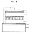
- Al is then deposited on the second cathode to form a first cathode, followed by hermetically sealing, thus completing the organic EL device according to the present invention shown in FIG. 1.
- an anode 12 is formed on a substrate 11, and a hole transport layer 13, an emitter layer 14, an electron transport layer 15, and a second cathode 16 and a first cathode 17 disposed in a predetermined pattern in a direction orthogonal to the anode 12, are sequentially stacked on the anode 12.
- the thickness of the second cathode 16 is 5 to 100 nm, and the thickness of the first cathode 17 is 10 to 150 nm.
- the second cathode 16 exhibits little difference in characteristic depending on thickness. However, if the thickness of the second cathode 16 is less than 5 nm, the electron injection efficiency deteriorates. If the thickness of the second cathode 16 is greater than 100 nm, drive deterioration occurs. If the thickness of the first cathode 17 is less than 10 nm, sheet resistance increases, resulting in drive deterioration. If the thickness of the first cathode 17 is greater than 150 nm, thin film formation is difficult to achieve.
- An organic EL device can be manufactured in the above-described order, that is, anode/hole transport layer/emitter layer/electron transport layer/cathode, and may be manufactured in the reverse order, that is, cathode/electron transport layer/ emitter layer/ hole transport layer/anode.
- the substrate is not necessarily a transparent material, and the aperture ratio becomes advantageously high.
- a substrate that can be used for a conventional organic EL device preferably a glass substrate or transparent plastic substrate having good transparency, surface smoothness, manageability and being waterproof, is used.
- anode forming materials indium tin oxide (ITO), tin oxide (SnO 2 ) or zinc oxide (ZnO), which is transparent and has good conductivity, is used.
- the thickness of the anode is 100 to 200 nm. If the thickness of the anode is greater than the above range, drive deterioration occurs due to sheet resistance and optical properties of the anode undesirably change.
- ITO (indium-tin-oxide) electrode layer was formed on a glass substrate to a thickness of 15 nm, and IDE 406 (manufactured by IDEMITSU KASAN LTD.) was vacuum-deposited thereon, to form a hole injection layer having a thickness of 50 nm. Subsequently, NPB was vacuum-deposited on the hole injection layer, to form a hole transport layer having a thickness of 15 nm.
- Alq 3 was vacuum-deposited on the hole transport layer to form an electron transport layer having a thickness of 70 nm.
- Al and Cs acetate mixed in a weight ratio of 10:1 were thermally deposited on the electron transport layer to form a second cathode to a thickness of 30 nm.
- Al was vacuum-deposited on the second cathode to form a first cathode having a thickness of 70 nm.
- the resultant product was hermetically sealed, thus completing an organic EL device.
- Example 2 The same procedure as Example 1 was performed except that Al and Cs acetate were mixed in a weight ratio of 5:1, thus completing an organic EL device.
- Example 2 The same procedure as Example 1 was performed except that In and Cs acetate were used for the manufacture of the second cathode, instead of Al and Cs acetate, thus completing an organic EL device.
- Example 2 The same procedure as Example 1 was performed except that Cr and Cs acetate were used for the manufacture of the second cathode, instead of Al and Cs acetate, thus completing an organic EL device.
- Example 2 The same procedure as Example 1 was performed except that Ag and Cs acetate were used for the manufacture of the second cathode, instead of Al and Cs acetate, thus completing an organic EL device.
- Example 2 The same procedure as Example 1 was performed except that Al and Cs benzoate were used for the manufacture of the second cathode, instead of Al and Cs acetate, thus completing an organic EL device.
- ITO electrode was formed on a glass substrate to a thickness of 15 nm, and IDE 406 (manufactured by IDEMITSU KOSAN) was vacuum-deposited thereon, to form a hole injection layer having a thickness of 15 nm. Subsequently, NPB was vacuum-deposited on the hole injection layer, to form a hole transport layer having a thickness of 15 nm.
- IDE 120 manufactured by IDEMITSU KOSAN, LTD.
- IDE 105 manufactured by IDEMITSU KOSAN, LTD.
- Alq 3 was vacuum-deposited on the electron injection layer to form an electron transport layer having a thickness of 30 nm.
- Al and Cs acetate mixed in a weight ratio of 94:6 were thermally deposited on the electron transport layer to form a second cathode to a thickness of 30 nm.
- Al was vacuum-deposited on the second cathode to form a first cathode having a thickness of 70 nm.
- the resultant product was hermetically sealed, thus completing an organic EL device.
- Example 7 The same procedure as Example 7 was performed except that Al and Cs acetate were mixed in a weight ratio of 92:8, thus completing an organic EL device.
- ITO layer was formed on a glass substrate to a thickness of 150 nm, and IDE 406 (manufactured by IDEMITSU KOSAN, LTD.) was vacuum-deposited thereon, to form a hole injection layer having a thickness of 50 nm. Subsequently, NPB was vacuum-deposited on the hole injection layer, to form a hole transport layer having a thickness of 15 nm.
- Alq 3 was vacuum-deposited on the hole transport layer to form an electron transport layer having a thickness of 70 nm.
- LiF was vacuum-deposited on the electron transport layer to form an LiF electron injection layer having a thickness of 1 nm, and Al was then vacuum-deposited on the LiF electron injection layer to form an Al electrode having a thickness of 150 nm.
- the resultant product was hermetically sealed, thus completing an organic EL device.
- ITO layer was formed on a glass substrate to a thickness of 15 nm, and IDE 406 (manufactured by IDEMITSU KOSAN, LTD) was vacuum-deposited thereon, to form a hole injection layer having a thickness of 15 nm. Subsequently, NPB was vacuum-deposited on the hole injection layer, to form a hole transport layer having a thickness of 15 nm.
- IDE 120 manufactured by IDEMITSU KOSAN, LTD.
- IDE 105 manufactured by IDEMITSU KOSAN, LTD.
- Alq 3 was vacuum-deposited on the electron injection layer to form an electron transport layer having a thickness of 30 nm.
- LiF was vacuum-deposited on the electron transport layer to form an LiF electron injection layer having a thickness of 1 nm
- Al was then vacuum-deposited on the LiF electron injection layer to form an Al electrode having a thickness of 150 nm.
- the resultant product was hermetically sealed, thus completing an organic EL device.
- ITO layer was formed on a glass substrate to a thickness of 15 nm, and IDE 406 (manufactured by IDEMITSU KOSAN, LTD.) was vacuum-deposited thereon, to form a hole injection layer having a thickness of 15 nm. Subsequently, NPB was vacuum-deposited on the hole injection layer, to form a hole transport layer having a thickness of 15 nm.
- Alq 3 was vacuum-deposited on the hole transport layer to form an electron transport layer having a thickness of 30 nm.
- Li acetate was thermally deposited on the electron transport layer to form an electron injection layer, and Al was then vacuum-deposited on the electron injection layer to form an Al electrode having a thickness of 150 nm.
- the resultant product was hermetically sealed, thus completing an organic EL device.
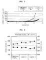
- the organic EL devices manufactured in Examples 1 and 2 exhibited a reduced driving voltage, and substantially the same levels of maximum luminance, electroluminescence efficiency and color coordinate characteristics as those of the organic EL device manufactured in Comparative Example 1.
- the organic EL devices manufactured in Examples 3 through 6 exhibited substantially the same levels of driving voltage, maximum luminance, electroluminescence efficiency and color coordinate characteristics as those of the organic EL device manufactured in Example 1.
- the organic EL devices manufactured in Examples 1 and 2 had larger current densities than the current density of the organic EL device manufactured in Comparative Example 1, confirming enhanced electron injection.
- the organic EL devices manufactured in Examples 7 and 8 exhibited a reduced driving voltage, and substantially the same levels of maximum luminance, emitting efficiency, power efficiency and color coordinate characteristics as those of the organic EL device manufactured in Comparative Example 2.
- the organic EL devices manufactured in Examples 7 and 8 had larger current densities than the current density of the organic EL device manufactured in Comparative Example 2, confirming enhanced electron injection.
- the organic EL devices manufactured in Examples 7 and 8 had higher luminance than the organic EL device manufactured in Comparative Example 2.
- the life characteristics of the compared organic EL devices are substantially the same.
- the luminance characteristics of the organic EL devices manufactured in Examples 7 and 8 are superior to those of the organic EL device manufactured in Comparative Example 2, it can be confirmed that the lifetimes of the organic EL devices manufactured in Examples 7 and 8 were longer than the lifetime of the organic EL device manufactured in Comparative Example 2, under the same luminance level.
- the organic EL devices manufactured in Examples 1 and 2 exhibited substantially the same levels of driving voltage and color coordinate characteristics, but were superior to the organic EL device manufactured in Comparative Example 3 in view of maximum luminance and electroluminescence efficiency.
- the organic EL devices manufactured in Examples 1 and 2 had larger current densities than the current density of the organic EL device manufactured in Comparative Example 3, confirming enhanced electron injection.
- the lifetimes of the organic EL devices manufactured in Examples 1 and 2 are longer than that of the organic EL device manufactured in Comparative Examples 3.
- the organic EL device In the organic EL device according to the present invention, an energy barrier difference between an electron transport layer and a cathode is reduced, thus enhancing an electron injection efficiency. Therefore, the organic EL device has a reduced driving voltage, while exhibiting good emitting efficiency, color coordinate and luminance characteristics.
Abstract
Description
- The present invention relates to an organic electroluminescent (EL) device, and more particularly, to an organic electroluminescent device having an improved efficiency of injecting electrons from a cathode to an organic layer.
- Recently, much attention has been paid to electroluminescent devices because they have advantageous features suitable for next generation display devices, such as a wide viewing angle, a high contrast ratio and a high response speed. In particular, organic electroluminescent devices using organic materials as raw materials for light emitting layers have advantageous characteristics, including a high luminance, a low driving voltage, a fast response rate, ability of producing a wide range of colors, compared to inorganic electroluminescent devices using inorganic materials as raw materials for light emitting layers.
- An organic electroluminescent (EL) device is basically configured such that an anode is formed on a substrate, and a hole transport layer, an emitter layer, an electron transport layer, and a cathode are sequentially stacked on the anode. Here, the hole transport layer, the emitter layer and the electron transport layer are organic layers made of organic materials.
- In the organic EL device having the above-described configuration, if a voltage is applied to the anode and the cathode, holes injected from the anode migrate to the emitter layer via the hole transport layer, and electrons from the cathode are injected into the emitter layer via the electron transport layer. The electrons and holes are recombined at the interface between the hole transport layer and the emitter layer (or the electron transport layer) to generate excitons. The generated excitons de-excite from an excited state to a ground state causing fluorescent molecules of the emitter layer to emit light, thus forming an image.
- In the organic EL device driven as described above, to improve a low driving voltage characteristic and charge balance between electrons and holes, it is necessary to increase an efficiency of injecting electrons from a cathode into an organic layer, e.g., an electron transport layer, from a cathode. Conventional methods for increasing such injection efficiency have been proposed in U.S. Patent Nos. 5,429,884, 5,059,862 and 4,885,211, describing use of an alkali metal having a low work function, e. g., lithium or magnesium, codeposition of an alkali metal and a metal such as aluminum or silver, and use of alloys of an alkali metal and a metal such as aluminum or silver, respectively.
- However, the conventional methods have several problems. That is, since the metal that has a low work function is very unstable and highly reactive, use of the metal is disadvantageous in view of the processibility and the stability of EL device. In the case of codeposition, it is substantially difficult to control the mixture ratio of materials for forming an alloy. Also, use of alkali metals deteriorates reproducibility.
- Other techniques for increasing the electron injection efficiency have been proposed in U.S. Patent Nos. 5,776,622, 5,776,623, 5,937,272 and 5,739,635, and Appl. Phy Lett. 73 (1998) 1185, in which an electron injection layer containing inorganic materials such as LiF, CsF, SrO or Li2O, is formed between a cathode and an organic layer to a thickness of 5 to 20 Å. However, according to these techniques, inorganic material film formation requires an extremely high temperature, and it is quite difficult to form a thin film having a uniform thickness of 5 to 20 Å.
- Recently, another method for increasing an electron injection efficiency has been proposed in which an alkali metal acetate, e.g., CH3COOLi or C6H5COOLi, is formed between a cathode and an organic layer to a thickness of 5 to 40 Å. This method also has a problem in that it is difficult to form a thin film having a uniform thickness of 5 to 40 Å, which is not suitable for large-area deposition.
- As described above, various attempts for enhancing electron injection have conventionally been made, but no satisfactory technique has been found yet in view of processibility, driving voltage and efficiency.
- To overcome the above and/or other problems, the present invention provides an organic EL device with a reduced driving voltage, enhanced luminance and improved color coordinate characteristics by increasing an efficiency of injecting electrons from a cathode into an organic layer.
- In an aspect of the present invention, an organic EL device includes a cathode, an anode, and organic layers formed between the cathode and the anode. In the organic EL device, the cathode includes a first cathode containing aluminum, and a second cathode disposed under the first cathode, formed in the vicinity of an organic layer and containing a metal having a work function of 3.5 to 5.0 eV, and metallic carboxylate represented by:
- Additional aspects and advantages of the invention will be set forth in part in the description which follows and, in part, will be obvious from the description, or may be learned by practice of the invention.
- These and/or other aspects and advantages of the present invention will become apparent and more readily appreciated from the following description of the embodiments, taken in conjunction with the accompanying drawings of which:
- FIG. 1 is a schematic diagram of an organic EL device according to the present invention;
- FIG. 2A is an energy band diagram representing an energy gap between the highest occupied molecular orbital (HOMO) of an electron transport layer and the lowest unoccupied molecular orbital LUMO of a cathode, in an organic EL device including a hole injection layer made of IDE 406 (manufactured by IDEMITSU KOSAN, LTD.), a hole transport layer made of N,N'-diphenyl-N,N'-bis(1-naphthyl)-1,1'-biphenyl)-4,4'-diamine (NPB), an electron transport layer made of Alq3, an electron injection layer made of LiF, and a cathode made of Al, and FIG. 2B is an energy band diagram representing an energy gap between the HOMO of an electron transport layer and the LUMO of a cathode, in an organic EL device including a hole injection layer made of IDE 406 (manufactured by IDEMITSU KOSAN, LTD.), a hole transport layer made of NPB, an electron transport layer made of Alq3, and a second cathode disposed in the vicinity of the electron transport layer and made of cesium acetate and Al;
- FIG. 3 shows driving voltage and efficiency characteristics of organic EL devices prepared in Examples 1-2 of the present invention and Comparative Example 1;
- FIG. 4 shows color coordinate characteristics of organic EL devices prepared in Examples 1-2 of the present invention and Comparative Example 1;
- FIG. 5 shows voltage versus current density characteristics of organic EL devices prepared in Examples 1-2 of the present invention and Comparative Example 1;
- FIG. 6 shows driving voltage and efficiency characteristics of organic EL devices prepared in Examples 7-8 of the present invention and Comparative Example 2;
- FIG. 7 shows color coordinate characteristics of organic EL devices prepared in Examples 7-8 of the present invention and Comparative Example 2;
- FIG. 8 shows voltage versus current density characteristics of organic EL devices prepared in Examples 7-8 of the present invention and Comparative Example 2;
- FIG. 9 shows voltage versus luminance characteristics of organic EL devices prepared in Examples 7-8 of the present invention and Comparative Example 2;
- FIG. 10 shows life characteristics of organic EL devices prepared in Examples 7-8 of the present invention and Comparative Example 2;
- FIG. 11 shows driving voltage and efficiency characteristics of organic EL devices prepared in Examples 1-2 of the present invention and Comparative Example 3;
- FIG. 12 shows voltage versus current density characteristics of organic EL devices prepared in Examples 1-2 of the present invention and Comparative Example 3; and
- FIG. 13 shows life characteristics of organic EL devices prepared in Examples 1-2 of the present invention and Comparative Example 3.
-
- Reference will now be made in detail to the present preferred embodiments of the present invention, examples of which are illustrated in the accompanying drawings, wherein like reference numerals refer to the like elements throughout. The embodiments are described below in order to explain the present invention by referring to the figures.
- A cathode of the present invention has a bi-layer structure including a first cathode made of Al, and a second cathode containing a cathode forming metal having a work function of 3.5 to 5.0 eV and metallic carboxylate represented by Formula 1. The second cathode is disposed under the first cathode and formed in the vicinity of an organic layer. Examples of the metal having a work function of 3.5 to 5.0 eV include indium (In) (work function: 3.8-4.2 eV), chrome (Cr) (work function: 4.3 eV), aluminum (Al)(work function: 4.3 eV), silver (Ag) (4.6 eV), and Al is most preferred in view of processibility. If the work function of the cathode forming metal is less than 3.5 eV, the metal is unstable, resulting in poor processibility. If the work function of the cathode forming metal is greater than 5.0 eV, electron injection characteristics undesirably deteriorate.
- The metallic carboxylate represented by Formula 1 is an organic material in which a metal (M) functions as the opposite ion to a carboxylate functional group, and examples of the metal M include alkali or alkaline-earth metals having a work function of 4.0 eV or less, specifically 1 to 4.0 eV. The metal is preferably an alkali metal such as lithium (Li), sodium (Na), potassium (K), rubidium (Rb) or cesium (Cs).
Formula 1, the C1-C10 alkyl is preferably a methyl or ethyl group, and the C6-C20 aryl is preferably a phenyl group. - The metallic carboxylate of the present invention is preferably lithium acetate (CH3COOLi), lithium benzoate (C6H5COOLi), potassium acetate (CH3COOK), potassium benzoate (C6H5COOK), cesium benzoate (C6H5COOCs), cesium acetate (CH3COOCs), sodium benzoate (C6H5COONa), sodium acetate (CH3COONa), rubidium benzoate (C6H5COORb) or rubidium acetate (CH3COORb).
- In the second cathode, the mixture ratio of the cathode forming metal to the metallic carboxylate is preferably 1:1 to 10: 0.1, more preferably 5:1 to 15:1, and most preferably 10:1.
- Now, the principle of the present invention will be briefly described referring to FIGS. 2A and 2B, in which IDE 406 (manufactured by IDEMITSU KOSAN, LTD.) is used for forming a hole injection layer, NPB is used for forming a hole transport layer, Alq3 is used for forming an electron transport layer, and the second cathode disposed in the vicinity of the electron transport layer is made of Al and cesium acetate.
- The organic EL device shown in FIG. 2A including the electron injection layer (LiF) adjacent to the electron transport layer (Alq3) and the cathode (Al) has an improved electron injection efficiency in an organic layer by a reduced energy barrier height or electron tunneling at the interface between an organic layer and LiF, due to a band bending phenomenon in which the LUMO level of Alq3 is lowered from the interface. In this case, since there is a big energy difference between the LUMO level of Alq3, i.e., 3.0 eV, and the work function level of a cathode, i.e., 4.3 eV, electron injection is not effective due to band bending or electron tunneling. On the other hand, in the organic EL device shown in FIG. 2B, since the second cathode adjacent to the electron transport layer (Alq3) includes Al and cesium acetate, and there is little energy difference between the LUMO of Alq3, i.e., 3.0 eV, and the work function of the cathode, i.e., approximately 3.0 eV, electron injection into an organic layer from the cathode is enhanced even with a low voltage applied.
- A method of manufacturing the organic EL device according to the present invention is described below. First, an anode is formed on a substrate and then a hole injection layer is selectively formed on the anode. The hole injection layer decreases contact resistance between the anode and a hole transport layer and increases the hole transporting capability of the anode with respect to an emitter layer (or electron transport layer), thus improving overall characteristics of the device. Usable materials to form the hole injection layer include starburst amine series compounds. The thickness of the hole injection layer is 30 to 100 nm. If the thickness of the hole injection layer is out of the above range, hole injection characteristics are undesirably poor.
- Then, a hole transport layer is formed on the hole injection layer. Hole transporting materials to form the hole transport layer include N,N'-di(naphthalene-1-yl)-N,N'-diphenyl-benzidine: α-NPB, -4,4'-diamine] N,N'-bis(3-methylphenyl)-N,N'-diphenyl-(1,1'-biphenyl)-4,4'-diamine (TPD) and the like . The thickness of the hole transport layer is 10 to 50 nm. If the thickness of the hole transport layer is out of the above range, hole injection characteristics are undesirably poor.
- In addition to the hole transporting material, the hole transport layer may further include a dopant capable of emitting light at electron-hole combination. Examples of the dopant include 4-(dicyanomethylene)-2-t-butyl-6-(1,1,7,7-tetramethyljulolidyl-9-enyl)-4H-pyran: DCJTB,
Coumarin 6, Rubrene, DCM, DCJTB, perylene, quinacridone or the like. The amount of the dopant is 0.1 to 5% by weight based on the weight of the hole transport layer forming material. Use of such a dopant in forming the hole transport layer allows the emitting color to be adjusted according to the kind and content of dopant added, and increases thermal stability of the hole transporting layer, thus improving the life of the device.
- Then, an emitter layer and/or an electron transport layer are formed on the hole transport layer. In an embodiment of the present invention, the emitter layer is not separately formed, but only the electron transport layer serving as an emitter layer is formed.
- As electron transporting materials to form the electron transport layer, tris(8-quinolinolate)-aluminum (Alq3) and Almq3 having the following formulas can be used, and a dopant capable of emitting light with respect to electron-hole combination, like the hole transport layer, may be further added. The kind and content of dopant added are substantially the same as those for the hole transport layer. The thickness of the electron transport layer is preferably 30 to 100 nm. If the thickness of the electron transport layer is out of the above range, the efficiency is lowered and a driving voltage increases, which are undesired.

- Thereafter, codeposition between a cathode forming metal having a work function of 3.5 to 5.0 eV and metallic carboxylate is performed on the emitter layer and/or electron transport layer, thus forming a second cathode. The codeposition method is not specifically limited, but thermal deposition is employed in the present invention.
- Preferably, the cathode forming material and the metallic carboxylate having the
Formula 1 in the second cathode are mixed in the weight ratio of 1:1 to 10:0.1, more preferably 5:1 to 10:1. If the amount ratio of the metallic carboxylate to the cathode forming material is greater than the above range, the driving voltage increase. If the amount ratio of the metallic carboxylate to the cathode forming material is less than the above range, the electron injection efficiency is undesirably reduced. - Al is then deposited on the second cathode to form a first cathode, followed by hermetically sealing, thus completing the organic EL device according to the present invention shown in FIG. 1.
- Referring to FIG. 1, an
anode 12 is formed on asubstrate 11, and ahole transport layer 13, anemitter layer 14, anelectron transport layer 15, and a second cathode 16 and afirst cathode 17 disposed in a predetermined pattern in a direction orthogonal to theanode 12, are sequentially stacked on theanode 12. - The thickness of the second cathode 16 is 5 to 100 nm, and the thickness of the
first cathode 17 is 10 to 150 nm. The second cathode 16 exhibits little difference in characteristic depending on thickness. However, if the thickness of the second cathode 16 is less than 5 nm, the electron injection efficiency deteriorates. If the thickness of the second cathode 16 is greater than 100 nm, drive deterioration occurs. If the thickness of thefirst cathode 17 is less than 10 nm, sheet resistance increases, resulting in drive deterioration. If the thickness of thefirst cathode 17 is greater than 150 nm, thin film formation is difficult to achieve. - An organic EL device can be manufactured in the above-described order, that is, anode/hole transport layer/emitter layer/electron transport layer/cathode, and may be manufactured in the reverse order, that is, cathode/electron transport layer/ emitter layer/ hole transport layer/anode. In the latter case, the substrate is not necessarily a transparent material, and the aperture ratio becomes advantageously high.
- In the organic EL device according to the present invention, a substrate that can be used for a conventional organic EL device, preferably a glass substrate or transparent plastic substrate having good transparency, surface smoothness, manageability and being waterproof, is used. As anode forming materials, indium tin oxide (ITO), tin oxide (SnO2) or zinc oxide (ZnO), which is transparent and has good conductivity, is used. The thickness of the anode is 100 to 200 nm. If the thickness of the anode is greater than the above range, drive deterioration occurs due to sheet resistance and optical properties of the anode undesirably change.
- The present invention will be further described with reference to the following examples however, it should be noted that the present invention is not restricted by these examples.
- An ITO (indium-tin-oxide) electrode layer was formed on a glass substrate to a thickness of 15 nm, and IDE 406 (manufactured by IDEMITSU KASAN LTD.) was vacuum-deposited thereon, to form a hole injection layer having a thickness of 50 nm. Subsequently, NPB was vacuum-deposited on the hole injection layer, to form a hole transport layer having a thickness of 15 nm.
- Thereafter, Alq3 was vacuum-deposited on the hole transport layer to form an electron transport layer having a thickness of 70 nm. Al and Cs acetate mixed in a weight ratio of 10:1 were thermally deposited on the electron transport layer to form a second cathode to a thickness of 30 nm. Then, Al was vacuum-deposited on the second cathode to form a first cathode having a thickness of 70 nm.
- The resultant product was hermetically sealed, thus completing an organic EL device.
- The same procedure as Example 1 was performed except that Al and Cs acetate were mixed in a weight ratio of 5:1, thus completing an organic EL device.
- The same procedure as Example 1 was performed except that In and Cs acetate were used for the manufacture of the second cathode, instead of Al and Cs acetate, thus completing an organic EL device.
- The same procedure as Example 1 was performed except that Cr and Cs acetate were used for the manufacture of the second cathode, instead of Al and Cs acetate, thus completing an organic EL device.
- The same procedure as Example 1 was performed except that Ag and Cs acetate were used for the manufacture of the second cathode, instead of Al and Cs acetate, thus completing an organic EL device.
- The same procedure as Example 1 was performed except that Al and Cs benzoate were used for the manufacture of the second cathode, instead of Al and Cs acetate, thus completing an organic EL device.
- An ITO electrode was formed on a glass substrate to a thickness of 15 nm, and IDE 406 (manufactured by IDEMITSU KOSAN) was vacuum-deposited thereon, to form a hole injection layer having a thickness of 15 nm. Subsequently, NPB was vacuum-deposited on the hole injection layer, to form a hole transport layer having a thickness of 15 nm.
- Thereafter, IDE 120 (manufactured by IDEMITSU KOSAN, LTD.) and IDE 105 (manufactured by IDEMITSU KOSAN, LTD.) mixed in a weight ratio of 97:3 were codeposited on the hole transport layer to form an electron injection layer having a thickness of 30 nm. Alq3 was vacuum-deposited on the electron injection layer to form an electron transport layer having a thickness of 30 nm.
- Then, Al and Cs acetate mixed in a weight ratio of 94:6 were thermally deposited on the electron transport layer to form a second cathode to a thickness of 30 nm. Subsequently, Al was vacuum-deposited on the second cathode to form a first cathode having a thickness of 70 nm.
- The resultant product was hermetically sealed, thus completing an organic EL device.
- The same procedure as Example 7 was performed except that Al and Cs acetate were mixed in a weight ratio of 92:8, thus completing an organic EL device.
- An ITO layer was formed on a glass substrate to a thickness of 150 nm, and IDE 406 (manufactured by IDEMITSU KOSAN, LTD.) was vacuum-deposited thereon, to form a hole injection layer having a thickness of 50 nm. Subsequently, NPB was vacuum-deposited on the hole injection layer, to form a hole transport layer having a thickness of 15 nm.
- Thereafter, Alq3 was vacuum-deposited on the hole transport layer to form an electron transport layer having a thickness of 70 nm. LiF was vacuum-deposited on the electron transport layer to form an LiF electron injection layer having a thickness of 1 nm, and Al was then vacuum-deposited on the LiF electron injection layer to form an Al electrode having a thickness of 150 nm.
- The resultant product was hermetically sealed, thus completing an organic EL device.
- An ITO layer was formed on a glass substrate to a thickness of 15 nm, and IDE 406 (manufactured by IDEMITSU KOSAN, LTD) was vacuum-deposited thereon, to form a hole injection layer having a thickness of 15 nm. Subsequently, NPB was vacuum-deposited on the hole injection layer, to form a hole transport layer having a thickness of 15 nm.
- Thereafter, IDE 120 (manufactured by IDEMITSU KOSAN, LTD.) and IDE 105 (manufactured by IDEMITSU KOSAN, LTD.) mixed in a weight ratio of 97:3 were codeposited on the hole transport layer to form an electron injection layer having a thickness of 30 nm. Alq3 was vacuum-deposited on the electron injection layer to form an electron transport layer having a thickness of 30 nm.
- Then, LiF was vacuum-deposited on the electron transport layer to form an LiF electron injection layer having a thickness of 1 nm, and Al was then vacuum-deposited on the LiF electron injection layer to form an Al electrode having a thickness of 150 nm.
- The resultant product was hermetically sealed, thus completing an organic EL device.
- An ITO layer was formed on a glass substrate to a thickness of 15 nm, and IDE 406 (manufactured by IDEMITSU KOSAN, LTD.) was vacuum-deposited thereon, to form a hole injection layer having a thickness of 15 nm. Subsequently, NPB was vacuum-deposited on the hole injection layer, to form a hole transport layer having a thickness of 15 nm.
- Thereafter, Alq3 was vacuum-deposited on the hole transport layer to form an electron transport layer having a thickness of 30 nm.
- Subsequently, Li acetate was thermally deposited on the electron transport layer to form an electron injection layer, and Al was then vacuum-deposited on the electron injection layer to form an Al electrode having a thickness of 150 nm.
- The resultant product was hermetically sealed, thus completing an organic EL device.
- In the organic EL devices manufactured in Examples 1-2 and Comparative Example 1, driving voltage, maximum luminance, emitting efficiency and color coordinate characteristics were evaluated. The evaluation was performed under the current density of 10 to 100 mA/cm2.
- The evaluation results are shown in Table 1 and FIGs. 3 and 4.
Driving Maximum luminance Emiting efficiency C.I.E. voltage (V) (cd/m2) (cd/A) x y Example 1 13.24 4349 4.35 0.340 0.539 Example 2 10.29 4109 4.11 0.348 0.539 Comparative Example 1 14.25 4221 4.22 0.342 0.530 - As shown in Table 1 and FIGs. 3 and 4, the organic EL devices manufactured in Examples 1 and 2 exhibited a reduced driving voltage, and substantially the same levels of maximum luminance, electroluminescence efficiency and color coordinate characteristics as those of the organic EL device manufactured in Comparative Example 1.
- Also, the organic EL devices manufactured in Examples 3 through 6 exhibited substantially the same levels of driving voltage, maximum luminance, electroluminescence efficiency and color coordinate characteristics as those of the organic EL device manufactured in Example 1.
- In the organic EL devices manufactured in Examples 1 and 2 and Comparative Examples 1, a change in current density depending on voltage is shown in FIG. 5.
- Referring to FIG. 5, at the same voltage level, the organic EL devices manufactured in Examples 1 and 2 had larger current densities than the current density of the organic EL device manufactured in Comparative Example 1, confirming enhanced electron injection.
- In the organic EL devices manufactured in Examples 7 and 8 and Comparative Examples 2, driving voltage, maximum luminance, emitting efficiency, power efficiency and color coordinate characteristics were evaluated. The evaluation was performed under the current density of 10 to 100 mA/cm2.
- The evaluation results are shown in Table 2 and FIGS. 5 and 6.
Driving voltage (V) Maximum luminance (cd/m2) Emitting efficiency (cd/A) Power efficiency (Im/W) C.I.E. X Y Example 7 8.01 4277 4.28 1.66 0.151 0.144 8.03 4257 4.26 1.65 0.151 0.144 Example 8 7.94 4305 4.31 1.70 0.151 0.145 8.00 4344 4.34 1.71 0.152 0.148 Comparative Example 2 8.07 4192 4.19 1.63 0.154 0.147 8.05 4205 4.21 1.64 0.155 0.150 - As shown in Table 2 and FIGs. 5 and 6, the organic EL devices manufactured in Examples 7 and 8 exhibited a reduced driving voltage, and substantially the same levels of maximum luminance, emitting efficiency, power efficiency and color coordinate characteristics as those of the organic EL device manufactured in Comparative Example 2.
- In the organic EL devices manufactured in Examples 7 and 8 and Comparative Examples 2, a change in current density depending on voltage is shown in FIG. 8.
- Referring to FIG. 8, at the same voltage level, the organic EL devices manufactured in Examples 7 and 8 had larger current densities than the current density of the organic EL device manufactured in Comparative Example 2, confirming enhanced electron injection.
- In the organic EL devices manufactured in Examples 7 and 8 and Comparative Examples 2, a change in luminance depending on voltage is shown in FIG. 9.
- Referring to FIG. 9, at the same voltage level, the organic EL devices manufactured in Examples 7 and 8 had higher luminance than the organic EL device manufactured in Comparative Example 2.
- Also, in the organic EL devices manufactured in Examples 7 and 8 and Comparative Examples 2, life characteristics thereof were examined, and the results are shown in FIG. 10. The life characteristics were measured under the same current density (45.45 mA/cm2).
- Referring to FIG. 10, under the same current density, the life characteristics of the compared organic EL devices are substantially the same. However, since the luminance characteristics of the organic EL devices manufactured in Examples 7 and 8 are superior to those of the organic EL device manufactured in Comparative Example 2, it can be confirmed that the lifetimes of the organic EL devices manufactured in Examples 7 and 8 were longer than the lifetime of the organic EL device manufactured in Comparative Example 2, under the same luminance level.
- In the organic EL devices manufactured in Examples 1 and 2 and Comparative Examples 3, driving voltage, maximum luminance, emitting efficiency and color coordinate characteristics were evaluated. The evaluation was performed under the current density of 10 to 100 mA/cm2.
- The evaluation results are shown in Table 3 and FIG. 11.
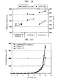
Driving voltage (V) Maximum Luminance( cd/m2) Emitting efficiency (cd/A) Power efficiency (Im/W) C.I.E. x y Example 1 8.01 4277 4.28 1.66 0.151 0.144 8.03 4257 4.26 1.65 0.151 0.144 Example 2 7.94 4305 4.31 1.70 0.151 0.145 8.00 4344 4.34 1.71 0.152 0.148 Comparative Example 3 7.92 4016 4.02 1.59 0.151 0.148 7.94 4026 4.03 1.59 0.151 0.151 - As shown in Table 3 and FIG. 11, the organic EL devices manufactured in Examples 1 and 2 exhibited substantially the same levels of driving voltage and color coordinate characteristics, but were superior to the organic EL device manufactured in Comparative Example 3 in view of maximum luminance and electroluminescence efficiency.
- In the organic EL devices manufactured in Examples 1 and 2 and Comparative Examples 3, a change in current density depending on voltage is shown in FIG. 12.
- Referring to FIG. 12, at the same voltage level, the organic EL devices manufactured in Examples 1 and 2 had larger current densities than the current density of the organic EL device manufactured in Comparative Example 3, confirming enhanced electron injection.
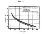
- Also, in the organic EL devices manufactured in Examples 1 and 2 and Comparative Examples 3, life characteristics thereof were examined, and the results are shown in FIG. 13. The life characteristics were measured under the same current density (45.45mA/cm2).
- Referring to FIG. 13, under the same luminance level, the lifetimes of the organic EL devices manufactured in Examples 1 and 2 are longer than that of the organic EL device manufactured in Comparative Examples 3.
- In the organic EL device according to the present invention, an energy barrier difference between an electron transport layer and a cathode is reduced, thus enhancing an electron injection efficiency. Therefore, the organic EL device has a reduced driving voltage, while exhibiting good emitting efficiency, color coordinate and luminance characteristics.
Claims (14)
- An organic electroluminescent (EL) device having a cathode, an anode, and organic layers formed between the cathode and the anode, wherein the cathode comprises:wherein M is an alkali metal or alkaline-earth metal, and R is a C1-C10 alkyl or C6-C20 aryl group.a first cathode containing aluminum; anda second cathode disposed under the first cathode, formed in a vicinity of one of the organic layers and containing a metal having a work function of 3.5 to 5.0 eV, and metallic carboxylate represented by:
- The organic EL device according to claim 1, wherein the metal having a work function of 3.5 to 5.0 eV is at least one of aluminum (Al), indium (In), chrome (Cr) and silver (Ag).
- The organic EL device according to claim 1 or 2, wherein in the metallic carboxylate represented by Formula 1, the metal is lithium (Li), sodium (Na), potassium (K), rubidium (Rb) or cesium (Cs).
- The organic EL device according to any of claims 1 to 3, wherein in Formula 1, R is a methyl, ethyl or phenyl group.
- The organic EL device according to claim 1, wherein the metallic carboxylate is at least one selected from lithium acetate (CH3COOLi), lithium benzoate (C6H5COOLi), potassium acetate (CH3COOK), potassium benzoate (C6H5COOK), cesium benzoate (C6H5COOCs), cesium acetate (CH3COOCs), sodium benzoate (C6H5COONa), sodium acetate (CH3COONa), rubidium benzoate (C6H5COORb) and rubidium acetate (CH3COORb).
- The organic EL device according to any of claims 1 to 5, wherein in the second cathode, the mixture ratio of Al to the metallic carboxylate represented by Formula 1 is 1:1 to 10: 0.1.
- The organic EL device according to claim 6, wherein in the second cathode, the mixture ratio of Al to the metallic carboxylate represented by Formula 1 is 5:1 to 10:1.
- The organic EL device according to any of claims 1 to 7, wherein the thickness of the first cathode is in the range of 10 to 150 nm, and the thickness of the second cathode is in the range of 5 to 100 nm.
- The organic EL device according to any of claims 1 to 8, wherein the organic layers include at least one selected from an electron transport layer, an emitter layer, a hole transport layer and a hole injection layer.
- The organic EL device according to any of claims 1 to 9, wherein the organic EL device comprises a display device in an electronic device.
- The organic EL device according to claim 10, wherein the electronic device is one of a pager, a cellular telephone, a portable telephone, a two-way radio, a video game, a portable digital assistant, a portable television, a portable computer, a notebook computer, a calculator, a computer, a telephone, a check-out device that registers purchases, a monitoring device, and a digital clock.
- The organic EL device according to any of claims 1 to 11, comprising an indium-tin-oxide electrode layer formed on a glass substrate to a thickness of approximately 15 nm, a hole injection layer having a thickness of approximately 50 nm vacuum deposited thereon, a hole transport layer having a thickness of approximately 15 nm vacuum-deposited on the hole injection layer, Alq3 vacuum-deposited on the hole transport layer to form an electron transport layer having a thickness of approximately 70 nm, Al and Cs acetate mixed in a weight ratio of 10:1 thermally deposited on the electron transport layer to form a second cathode to a thickness of approximately 30 nm, and Al vacuum-deposited on the second cathode to form a first cathode having a thickness of approximately 70 nm.
- The organic EL device according to any of claims 1 to 11, comprising an indium-tin-oxide electrode layer formed on a glass substrate to a thickness of approximately 15 nm, a hole injection layer having a thickness of approximately 50 nm vacuum deposited thereon, a hole transport layer having a thickness of approximately 15 nm vacuum-deposited on the hole injection layer, Alq3 vacuum-deposited on the hole transport layer to form an electron transport layer having a thickness of approximately 70 nm, Al and Cs acetate mixed in a weight ratio of 5:1 thermally deposited on the electron transport layer to form a second cathode to a thickness of approximately 30 nm, and Al vacuum-deposited on the second cathode to form a first cathode having a thickness of approximately 70 nm.
- The organic EL device according to any of claims 1 to 11, comprising an indium-tin-oxide electrode layer formed on a glass substrate to a thickness of approximately 15 nm, a hole injection layer having a thickness of approximately 50 nm vacuum deposited thereon, a hole transport layer having a thickness of approximately 15 nm vacuum-deposited on the hole injection layer, Alq3 vacuum-deposited on the hole transport layer to form an electron transport layer having a thickness of approximately 70 nm, Al and Cs benzoate mixed in a weight ratio of 10:1 thermally deposited on the electron transport layer to form a second cathode to a thickness of approximately 30 nm, and Al vacuum-deposited on the second cathode to form a first cathode having a thickness of approximately 70 nm.
Applications Claiming Priority (2)
| Application Number | Priority Date | Filing Date | Title |
|---|---|---|---|
| KR10-2002-0018500A KR100473283B1 (en) | 2002-04-04 | 2002-04-04 | Organic electroluminescence device |
| KR2002018500 | 2002-04-04 |
Publications (3)
| Publication Number | Publication Date |
|---|---|
| EP1351324A2 true EP1351324A2 (en) | 2003-10-08 |
| EP1351324A3 EP1351324A3 (en) | 2004-12-22 |
| EP1351324B1 EP1351324B1 (en) | 2012-12-12 |
Family
ID=28036196
Family Applications (1)
| Application Number | Title | Priority Date | Filing Date |
|---|---|---|---|
| EP20030252092 Expired - Fee Related EP1351324B1 (en) | 2002-04-04 | 2003-04-02 | Organic electroluminescent device comprising a metallic carboxylate |
Country Status (5)
| Country | Link |
|---|---|
| US (1) | US6803128B2 (en) |
| EP (1) | EP1351324B1 (en) |
| JP (1) | JP2003303691A (en) |
| KR (1) | KR100473283B1 (en) |
| CN (1) | CN1449227A (en) |
Cited By (1)
| Publication number | Priority date | Publication date | Assignee | Title |
|---|---|---|---|---|
| US10886497B2 (en) | 2003-12-26 | 2021-01-05 | Semiconductor Energy Laboratory Co., Ltd. | Light-emitting element |
Families Citing this family (14)
| Publication number | Priority date | Publication date | Assignee | Title |
|---|---|---|---|---|
| US7270894B2 (en) * | 2004-06-22 | 2007-09-18 | General Electric Company | Metal compound-metal multilayer electrodes for organic electronic devices |
| US8026510B2 (en) | 2004-10-20 | 2011-09-27 | Dai Nippon Printing Co., Ltd. | Organic electronic device and method for producing the same |
| US20070108900A1 (en) * | 2005-11-15 | 2007-05-17 | Boek Heather D | Method and apparatus for the elimination of interference fringes in an OLED device |
| US20070236140A1 (en) * | 2006-04-05 | 2007-10-11 | Hsiang-Lun Hsu | System for displaying images including electroluminescent device and method for fabricating the same |
| US20080024059A1 (en) * | 2006-07-27 | 2008-01-31 | Tpo Displays Corp. | System for displaying images incluidng electroluminescent device and method for fabricating the same |
| JP4629715B2 (en) * | 2006-12-06 | 2011-02-09 | 韓國電子通信研究院 | OLED element |
| US20090176010A1 (en) * | 2008-01-04 | 2009-07-09 | M Zwick Lucy | Method of manufacturing organic light emitting display |
| JP2009205985A (en) * | 2008-02-28 | 2009-09-10 | Sumitomo Chemical Co Ltd | Organic electroluminescent element, and its manufacturing method |
| WO2011024671A1 (en) * | 2009-08-26 | 2011-03-03 | コニカミノルタホールディングス株式会社 | Organic electroluminescent element |
| CN102005537A (en) * | 2010-09-17 | 2011-04-06 | 天津理工大学 | Organic photovoltaic cell using lithium benzoate as cathode modifying layer and preparation method thereof |
| KR101846410B1 (en) | 2011-07-29 | 2018-04-09 | 삼성디스플레이 주식회사 | Organic light emitting diode display |
| KR20130032675A (en) * | 2011-09-23 | 2013-04-02 | 삼성디스플레이 주식회사 | Dual mode organic light emitting device and pixel circuit including the same |
| CN103187540B (en) * | 2011-12-31 | 2019-07-09 | 昆山维信诺显示技术有限公司 | A kind of organic electroluminescence device and preparation method thereof |
| KR101986434B1 (en) * | 2017-12-08 | 2019-06-05 | 재단법인대구경북과학기술원 | Transparent luminous body, inorganic light emmiting device and organic light emmiting device |
Citations (4)
| Publication number | Priority date | Publication date | Assignee | Title |
|---|---|---|---|---|
| EP0822603A2 (en) | 1996-07-29 | 1998-02-04 | Eastman Kodak Company | Bilayer electron-injecting electrode for use in an electroluminescent device |
| US5739635A (en) | 1995-04-27 | 1998-04-14 | Pioneer Electric Corporation | Organic electroluminescent device |
| US5776623A (en) | 1996-07-29 | 1998-07-07 | Eastman Kodak Company | Transparent electron-injecting electrode for use in an electroluminescent device |
| US5937272A (en) | 1997-06-06 | 1999-08-10 | Eastman Kodak Company | Patterned organic layers in a full-color organic electroluminescent display array on a thin film transistor array substrate |
Family Cites Families (12)
| Publication number | Priority date | Publication date | Assignee | Title |
|---|---|---|---|---|
| US4885211A (en) | 1987-02-11 | 1989-12-05 | Eastman Kodak Company | Electroluminescent device with improved cathode |
| US5059862A (en) * | 1990-07-26 | 1991-10-22 | Eastman Kodak Company | Electroluminescent device with improved cathode |
| US5059861A (en) * | 1990-07-26 | 1991-10-22 | Eastman Kodak Company | Organic electroluminescent device with stabilizing cathode capping layer |
| US5429884A (en) | 1992-01-17 | 1995-07-04 | Pioneer Electronic Corporation | Organic electroluminescent element |
| JPH07122177A (en) * | 1993-10-25 | 1995-05-12 | Noritake Co Ltd | Oxide cathode |
| US5677572A (en) * | 1996-07-29 | 1997-10-14 | Eastman Kodak Company | Bilayer electrode on a n-type semiconductor |
| US6140763A (en) * | 1998-07-28 | 2000-10-31 | Eastman Kodak Company | Interfacial electron-injecting layer formed from a doped cathode for organic light-emitting structure |
| US6545359B1 (en) * | 1998-12-18 | 2003-04-08 | Semiconductor Energy Laboratory Co., Ltd. | Wiring line and manufacture process thereof, and semiconductor device and manufacturing process thereof |
| US6924594B2 (en) * | 2000-10-03 | 2005-08-02 | Semiconductor Energy Laboratory Co., Ltd. | Light emitting device |
| KR100579172B1 (en) * | 2000-10-11 | 2006-05-11 | 삼성에스디아이 주식회사 | Organic electro luminescence device |
| DE60132450T2 (en) * | 2001-09-04 | 2008-04-17 | Sony Deutschland Gmbh | Solar cell and manufacturing method |
| US6794061B2 (en) * | 2002-01-31 | 2004-09-21 | Eastman Kodak Company | Organic electroluminescent device having an adhesion-promoting layer for use with a magnesium cathode |
-
2002
- 2002-04-04 KR KR10-2002-0018500A patent/KR100473283B1/en not_active IP Right Cessation
-
2003
- 2003-03-24 US US10/394,066 patent/US6803128B2/en not_active Expired - Fee Related
- 2003-04-02 EP EP20030252092 patent/EP1351324B1/en not_active Expired - Fee Related
- 2003-04-04 CN CN03110203A patent/CN1449227A/en active Pending
- 2003-04-04 JP JP2003102009A patent/JP2003303691A/en active Pending
Patent Citations (5)
| Publication number | Priority date | Publication date | Assignee | Title |
|---|---|---|---|---|
| US5739635A (en) | 1995-04-27 | 1998-04-14 | Pioneer Electric Corporation | Organic electroluminescent device |
| EP0822603A2 (en) | 1996-07-29 | 1998-02-04 | Eastman Kodak Company | Bilayer electron-injecting electrode for use in an electroluminescent device |
| US5776622A (en) | 1996-07-29 | 1998-07-07 | Eastman Kodak Company | Bilayer eletron-injeting electrode for use in an electroluminescent device |
| US5776623A (en) | 1996-07-29 | 1998-07-07 | Eastman Kodak Company | Transparent electron-injecting electrode for use in an electroluminescent device |
| US5937272A (en) | 1997-06-06 | 1999-08-10 | Eastman Kodak Company | Patterned organic layers in a full-color organic electroluminescent display array on a thin film transistor array substrate |
Non-Patent Citations (3)
| Title |
|---|
| APPL. PHYLETT., vol. 73, 1998, pages 1185 |
| J. KRUEGER, ADV. MAT., no. 12, 2000, pages 447 - 451 |
| L.S. HUNG ET AL., APPL. PHYS. LETT., vol. 70, no. 2, 1997, pages 152 - 154 |
Cited By (1)
| Publication number | Priority date | Publication date | Assignee | Title |
|---|---|---|---|---|
| US10886497B2 (en) | 2003-12-26 | 2021-01-05 | Semiconductor Energy Laboratory Co., Ltd. | Light-emitting element |
Also Published As
| Publication number | Publication date |
|---|---|
| KR100473283B1 (en) | 2005-03-08 |
| CN1449227A (en) | 2003-10-15 |
| EP1351324A3 (en) | 2004-12-22 |
| EP1351324B1 (en) | 2012-12-12 |
| KR20030079457A (en) | 2003-10-10 |
| US20030190494A1 (en) | 2003-10-09 |
| JP2003303691A (en) | 2003-10-24 |
| US6803128B2 (en) | 2004-10-12 |
Similar Documents
| Publication | Publication Date | Title |
|---|---|---|
| US7157156B2 (en) | Organic light emitting device having improved stability | |
| US7002293B2 (en) | Organic light emitting diode with improved light emission through the cathode | |
| KR101221124B1 (en) | Oleds having inorganic material containing anode capping layer | |
| US6392339B1 (en) | Organic light emitting devices including mixed region | |
| KR101221141B1 (en) | OLEDs having improved luminance stability | |
| KR100893056B1 (en) | Display devices with organic-metal mixed layer | |
| US7049741B2 (en) | Organic light emitting diode with improved light emission through substrate | |
| KR101657222B1 (en) | Organic light emitting device | |
| US6803128B2 (en) | Organic electroluminescent device | |
| JP2005026121A (en) | Organic el element and manufacturing method of the same as well as organic el display | |
| US6902834B2 (en) | Organic electroluminescence device | |
| KR20060120504A (en) | Display device with metal-organic mixed layer anodes | |
| US6114055A (en) | Organic electroluminescent device with continuous organic medium containing rubrene | |
| US8274212B2 (en) | Organic light emitting device including first hole injection layer and second hole injection layer | |
| JP2009088525A (en) | Organic light emitting device | |
| JPH10335066A (en) | Organic electroluminescent element and flat panel display using this organic electroluminescent element | |
| JPH11329731A (en) | Organic electroluminescent element | |
| JP2004014512A (en) | Organic light emitting diode device | |
| US20090224656A1 (en) | Organic light-emitting device | |
| JPH11329730A (en) | Organic electroluminescent element | |
| JPH11251068A (en) | Organic electroluminescence element | |
| US6194089B1 (en) | Organic electroluminescent device with improved reliability | |
| JPH1095971A (en) | Organic electroluminescent element | |
| KR100622229B1 (en) | Luminescence display devices using the fullerene based carbon compounds and method for preparing the same | |
| JP2000106277A (en) | Organic electroluminescence element |
Legal Events
| Date | Code | Title | Description |
|---|---|---|---|
| PUAI | Public reference made under article 153(3) epc to a published international application that has entered the european phase |
Free format text: ORIGINAL CODE: 0009012 |
|
| AK | Designated contracting states |
Kind code of ref document: A2 Designated state(s): AT BE BG CH CY CZ DE DK EE ES FI FR GB GR HU IE IT LI LU MC NL PT RO SE SI SK TR |
|
| AX | Request for extension of the european patent |
Extension state: AL LT LV MK |
|
| PUAL | Search report despatched |
Free format text: ORIGINAL CODE: 0009013 |
|
| AK | Designated contracting states |
Kind code of ref document: A3 Designated state(s): AT BE BG CH CY CZ DE DK EE ES FI FR GB GR HU IE IT LI LU MC NL PT RO SE SI SK TR |
|
| AX | Request for extension of the european patent |
Extension state: AL LT LV MK |
|
| RAP1 | Party data changed (applicant data changed or rights of an application transferred) |
Owner name: SAMSUNG SDI CO., LTD. |
|
| 17P | Request for examination filed |
Effective date: 20050615 |
|
| AKX | Designation fees paid |
Designated state(s): DE FR GB |
|
| 17Q | First examination report despatched |
Effective date: 20080714 |
|
| RAP1 | Party data changed (applicant data changed or rights of an application transferred) |
Owner name: SAMSUNG MOBILE DISPLAY CO., LTD. |
|
| REG | Reference to a national code |
Ref country code: DE Ref legal event code: R079 Ref document number: 60342825 Country of ref document: DE Free format text: PREVIOUS MAIN CLASS: H01L0051200000 Ipc: H01L0051500000 |
|
| RIC1 | Information provided on ipc code assigned before grant |
Ipc: H01L 51/50 20060101AFI20120606BHEP Ipc: H01L 51/52 20060101ALI20120606BHEP |
|
| GRAP | Despatch of communication of intention to grant a patent |
Free format text: ORIGINAL CODE: EPIDOSNIGR1 |
|
| RAP1 | Party data changed (applicant data changed or rights of an application transferred) |
Owner name: SAMSUNG DISPLAY CO., LTD. |
|
| GRAS | Grant fee paid |
Free format text: ORIGINAL CODE: EPIDOSNIGR3 |
|
| GRAA | (expected) grant |
Free format text: ORIGINAL CODE: 0009210 |
|
| AK | Designated contracting states |
Kind code of ref document: B1 Designated state(s): DE FR GB |
|
| REG | Reference to a national code |
Ref country code: GB Ref legal event code: FG4D |
|
| REG | Reference to a national code |
Ref country code: DE Ref legal event code: R096 Ref document number: 60342825 Country of ref document: DE Effective date: 20130207 |
|
| PLBE | No opposition filed within time limit |
Free format text: ORIGINAL CODE: 0009261 |
|
| STAA | Information on the status of an ep patent application or granted ep patent |
Free format text: STATUS: NO OPPOSITION FILED WITHIN TIME LIMIT |
|
| 26N | No opposition filed |
Effective date: 20130913 |
|
| REG | Reference to a national code |
Ref country code: DE Ref legal event code: R097 Ref document number: 60342825 Country of ref document: DE Effective date: 20130913 |
|
| REG | Reference to a national code |
Ref country code: FR Ref legal event code: PLFP Year of fee payment: 13 |
|
| PGFP | Annual fee paid to national office [announced via postgrant information from national office to epo] |
Ref country code: GB Payment date: 20150410 Year of fee payment: 13 Ref country code: DE Payment date: 20150409 Year of fee payment: 13 |
|
| PGFP | Annual fee paid to national office [announced via postgrant information from national office to epo] |
Ref country code: FR Payment date: 20150413 Year of fee payment: 13 |
|
| REG | Reference to a national code |
Ref country code: DE Ref legal event code: R119 Ref document number: 60342825 Country of ref document: DE |
|
| GBPC | Gb: european patent ceased through non-payment of renewal fee |
Effective date: 20160402 |
|
| REG | Reference to a national code |
Ref country code: FR Ref legal event code: ST Effective date: 20161230 |
|
| PG25 | Lapsed in a contracting state [announced via postgrant information from national office to epo] |
Ref country code: FR Free format text: LAPSE BECAUSE OF NON-PAYMENT OF DUE FEES Effective date: 20160502 Ref country code: DE Free format text: LAPSE BECAUSE OF NON-PAYMENT OF DUE FEES Effective date: 20161101 Ref country code: GB Free format text: LAPSE BECAUSE OF NON-PAYMENT OF DUE FEES Effective date: 20160402 |