EP1351287A2 - Semiconductor device and method for manufacturing the same - Google Patents
Semiconductor device and method for manufacturing the same Download PDFInfo
- Publication number
- EP1351287A2 EP1351287A2 EP02025620A EP02025620A EP1351287A2 EP 1351287 A2 EP1351287 A2 EP 1351287A2 EP 02025620 A EP02025620 A EP 02025620A EP 02025620 A EP02025620 A EP 02025620A EP 1351287 A2 EP1351287 A2 EP 1351287A2
- Authority
- EP
- European Patent Office
- Prior art keywords
- semiconductor device
- gate electrode
- manufacturing
- silicon oxide
- film
- Prior art date
- Legal status (The legal status is an assumption and is not a legal conclusion. Google has not performed a legal analysis and makes no representation as to the accuracy of the status listed.)
- Withdrawn
Links
Images







Classifications
-
- H—ELECTRICITY
- H10—SEMICONDUCTOR DEVICES; ELECTRIC SOLID-STATE DEVICES NOT OTHERWISE PROVIDED FOR
- H10B—ELECTRONIC MEMORY DEVICES
- H10B12/00—Dynamic random access memory [DRAM] devices
- H10B12/01—Manufacture or treatment
- H10B12/02—Manufacture or treatment for one transistor one-capacitor [1T-1C] memory cells
- H10B12/05—Making the transistor
-
- H—ELECTRICITY
- H10—SEMICONDUCTOR DEVICES; ELECTRIC SOLID-STATE DEVICES NOT OTHERWISE PROVIDED FOR
- H10W—GENERIC PACKAGES, INTERCONNECTIONS, CONNECTORS OR OTHER CONSTRUCTIONAL DETAILS OF DEVICES COVERED BY CLASS H10
- H10W20/00—Interconnections in chips, wafers or substrates
- H10W20/01—Manufacture or treatment
- H10W20/071—Manufacture or treatment of dielectric parts thereof
- H10W20/098—Manufacture or treatment of dielectric parts thereof by filling between adjacent conductive parts
-
- H—ELECTRICITY
- H10—SEMICONDUCTOR DEVICES; ELECTRIC SOLID-STATE DEVICES NOT OTHERWISE PROVIDED FOR
- H10B—ELECTRONIC MEMORY DEVICES
- H10B12/00—Dynamic random access memory [DRAM] devices
- H10B12/01—Manufacture or treatment
- H10B12/09—Manufacture or treatment with simultaneous manufacture of the peripheral circuit region and memory cells
-
- H—ELECTRICITY
- H10—SEMICONDUCTOR DEVICES; ELECTRIC SOLID-STATE DEVICES NOT OTHERWISE PROVIDED FOR
- H10D—INORGANIC ELECTRIC SEMICONDUCTOR DEVICES
- H10D84/00—Integrated devices formed in or on semiconductor substrates that comprise only semiconducting layers, e.g. on Si wafers or on GaAs-on-Si wafers
- H10D84/01—Manufacture or treatment
- H10D84/0123—Integrating together multiple components covered by H10D12/00 or H10D30/00, e.g. integrating multiple IGBTs
- H10D84/0126—Integrating together multiple components covered by H10D12/00 or H10D30/00, e.g. integrating multiple IGBTs the components including insulated gates, e.g. IGFETs
- H10D84/013—Manufacturing their source or drain regions, e.g. silicided source or drain regions
- H10D84/0133—Manufacturing common source or drain regions between multiple IGFETs
-
- H—ELECTRICITY
- H10—SEMICONDUCTOR DEVICES; ELECTRIC SOLID-STATE DEVICES NOT OTHERWISE PROVIDED FOR
- H10D—INORGANIC ELECTRIC SEMICONDUCTOR DEVICES
- H10D84/00—Integrated devices formed in or on semiconductor substrates that comprise only semiconducting layers, e.g. on Si wafers or on GaAs-on-Si wafers
- H10D84/01—Manufacture or treatment
- H10D84/02—Manufacture or treatment characterised by using material-based technologies
- H10D84/03—Manufacture or treatment characterised by using material-based technologies using Group IV technology, e.g. silicon technology or silicon-carbide [SiC] technology
- H10D84/038—Manufacture or treatment characterised by using material-based technologies using Group IV technology, e.g. silicon technology or silicon-carbide [SiC] technology using silicon technology, e.g. SiGe
-
- H—ELECTRICITY
- H10—SEMICONDUCTOR DEVICES; ELECTRIC SOLID-STATE DEVICES NOT OTHERWISE PROVIDED FOR
- H10P—GENERIC PROCESSES OR APPARATUS FOR THE MANUFACTURE OR TREATMENT OF DEVICES COVERED BY CLASS H10
- H10P14/00—Formation of materials, e.g. in the shape of layers or pillars
- H10P14/60—Formation of materials, e.g. in the shape of layers or pillars of insulating materials
- H10P14/66—Formation of materials, e.g. in the shape of layers or pillars of insulating materials characterised by the type of materials
- H10P14/668—Formation of materials, e.g. in the shape of layers or pillars of insulating materials characterised by the type of materials the materials being characterised by the deposition precursor materials
- H10P14/6681—Formation of materials, e.g. in the shape of layers or pillars of insulating materials characterised by the type of materials the materials being characterised by the deposition precursor materials the precursor containing a compound comprising Si
- H10P14/6682—Formation of materials, e.g. in the shape of layers or pillars of insulating materials characterised by the type of materials the materials being characterised by the deposition precursor materials the precursor containing a compound comprising Si the compound being a silane, e.g. disilane, methylsilane or chlorosilane
-
- H—ELECTRICITY
- H10—SEMICONDUCTOR DEVICES; ELECTRIC SOLID-STATE DEVICES NOT OTHERWISE PROVIDED FOR
- H10W—GENERIC PACKAGES, INTERCONNECTIONS, CONNECTORS OR OTHER CONSTRUCTIONAL DETAILS OF DEVICES COVERED BY CLASS H10
- H10W20/00—Interconnections in chips, wafers or substrates
- H10W20/01—Manufacture or treatment
- H10W20/031—Manufacture or treatment of conductive parts of the interconnections
- H10W20/069—Manufacture or treatment of conductive parts of the interconnections by forming self-aligned vias or self-aligned contact plugs
-
- H—ELECTRICITY
- H10—SEMICONDUCTOR DEVICES; ELECTRIC SOLID-STATE DEVICES NOT OTHERWISE PROVIDED FOR
- H10W—GENERIC PACKAGES, INTERCONNECTIONS, CONNECTORS OR OTHER CONSTRUCTIONAL DETAILS OF DEVICES COVERED BY CLASS H10
- H10W20/00—Interconnections in chips, wafers or substrates
- H10W20/01—Manufacture or treatment
- H10W20/071—Manufacture or treatment of dielectric parts thereof
- H10W20/081—Manufacture or treatment of dielectric parts thereof by forming openings in the dielectric parts
-
- H—ELECTRICITY
- H10—SEMICONDUCTOR DEVICES; ELECTRIC SOLID-STATE DEVICES NOT OTHERWISE PROVIDED FOR
- H10W—GENERIC PACKAGES, INTERCONNECTIONS, CONNECTORS OR OTHER CONSTRUCTIONAL DETAILS OF DEVICES COVERED BY CLASS H10
- H10W20/00—Interconnections in chips, wafers or substrates
- H10W20/40—Interconnections external to wafers or substrates, e.g. back-end-of-line [BEOL] metallisations or vias connecting to gate electrodes
-
- H—ELECTRICITY
- H10—SEMICONDUCTOR DEVICES; ELECTRIC SOLID-STATE DEVICES NOT OTHERWISE PROVIDED FOR
- H10W—GENERIC PACKAGES, INTERCONNECTIONS, CONNECTORS OR OTHER CONSTRUCTIONAL DETAILS OF DEVICES COVERED BY CLASS H10
- H10W20/00—Interconnections in chips, wafers or substrates
- H10W20/40—Interconnections external to wafers or substrates, e.g. back-end-of-line [BEOL] metallisations or vias connecting to gate electrodes
- H10W20/45—Interconnections external to wafers or substrates, e.g. back-end-of-line [BEOL] metallisations or vias connecting to gate electrodes characterised by their insulating parts
- H10W20/48—Insulating materials thereof
-
- H—ELECTRICITY
- H10—SEMICONDUCTOR DEVICES; ELECTRIC SOLID-STATE DEVICES NOT OTHERWISE PROVIDED FOR
- H10P—GENERIC PROCESSES OR APPARATUS FOR THE MANUFACTURE OR TREATMENT OF DEVICES COVERED BY CLASS H10
- H10P14/00—Formation of materials, e.g. in the shape of layers or pillars
- H10P14/60—Formation of materials, e.g. in the shape of layers or pillars of insulating materials
- H10P14/63—Formation of materials, e.g. in the shape of layers or pillars of insulating materials characterised by the formation processes
- H10P14/6326—Deposition processes
- H10P14/6328—Deposition from the gas or vapour phase
- H10P14/6334—Deposition from the gas or vapour phase using decomposition or reaction of gaseous or vapour phase compounds, i.e. chemical vapour deposition
- H10P14/6336—Deposition from the gas or vapour phase using decomposition or reaction of gaseous or vapour phase compounds, i.e. chemical vapour deposition in the presence of a plasma [PECVD]
-
- H—ELECTRICITY
- H10—SEMICONDUCTOR DEVICES; ELECTRIC SOLID-STATE DEVICES NOT OTHERWISE PROVIDED FOR
- H10P—GENERIC PROCESSES OR APPARATUS FOR THE MANUFACTURE OR TREATMENT OF DEVICES COVERED BY CLASS H10
- H10P14/00—Formation of materials, e.g. in the shape of layers or pillars
- H10P14/60—Formation of materials, e.g. in the shape of layers or pillars of insulating materials
- H10P14/69—Inorganic materials
- H10P14/692—Inorganic materials composed of oxides, glassy oxides or oxide-based glasses
- H10P14/6921—Inorganic materials composed of oxides, glassy oxides or oxide-based glasses containing silicon
- H10P14/69215—Inorganic materials composed of oxides, glassy oxides or oxide-based glasses containing silicon the material being a silicon oxide, e.g. SiO2
-
- H—ELECTRICITY
- H10—SEMICONDUCTOR DEVICES; ELECTRIC SOLID-STATE DEVICES NOT OTHERWISE PROVIDED FOR
- H10P—GENERIC PROCESSES OR APPARATUS FOR THE MANUFACTURE OR TREATMENT OF DEVICES COVERED BY CLASS H10
- H10P14/00—Formation of materials, e.g. in the shape of layers or pillars
- H10P14/60—Formation of materials, e.g. in the shape of layers or pillars of insulating materials
- H10P14/69—Inorganic materials
- H10P14/692—Inorganic materials composed of oxides, glassy oxides or oxide-based glasses
- H10P14/6921—Inorganic materials composed of oxides, glassy oxides or oxide-based glasses containing silicon
- H10P14/6922—Inorganic materials composed of oxides, glassy oxides or oxide-based glasses containing silicon the material containing Si, O and at least one of H, N, C, F or other non-metal elements, e.g. SiOC, SiOC:H or SiONC
- H10P14/6923—Inorganic materials composed of oxides, glassy oxides or oxide-based glasses containing silicon the material containing Si, O and at least one of H, N, C, F or other non-metal elements, e.g. SiOC, SiOC:H or SiONC the material being boron or phosphorus doped silicon oxides, e.g. BPSG, BSG or PSG
Definitions
- the present invention relates to a semiconductor device in which a gate electrode is formed on a semiconductor substrate and a method for manufacturing the same, and is preferable to be applied to a fine semiconductor device having high aspect ratio of an area between the gate electrodes and in which a gate length is shortened.
- the BPSG film covers the gate electrode and has a characteristic that it has a high etching selection ratio with a silicon nitride film, which works as an etching stopper in forming a contact hole. If this BPSG film is used as the interlayer insulating film, it is possible to sufficiently respond to a SAC (Self Align Contact) technique applied according to the shortened gate length and distance between the gate electrodes.
- SAC Self Align Contact
- a so-called slit void occurs at the film-formation. If a contact hole is formed between the gate electrodes, adjacent contact holes make a short circuit due to the slit void, and therefore it is necessary to eliminate the slit void by melting, reflowing, and annealing the BPSG film.
- the HDP-USG film since a mixed gas of SiH 4 , O 2 , and Ar is used as a growth gas in its formation and the melting, reflowing, and annealing step at the high temperature after the film-formation, which is essential for the BPSG film, is not needed, the above-described demand for controlling the temperature is responded.
- a mixed gas of SiH 4 , O 2 , and Ar is used as a growth gas in its formation and the melting, reflowing, and annealing step at the high temperature after the film-formation, which is essential for the BPSG film, is not needed.
- the HDP-USG film since a mixed gas of SiH 4 , O 2 , and Ar is used as a growth gas in its formation and the melting, reflowing, and annealing step at the high temperature after the film-formation, which is essential for the BPSG film, is not needed, the above-described demand for controlling the temperature is responded.
- the HDP-USG film to respond to the
- the present invention has achieved in consideration of the problems described above, and it is an object of the present invention to provide a semiconductor device capable of, responding to the gate length and the distance between gate electrode structures which have been further shortened recently, securing sufficient ability of filling the area between the gate electrode structures while maintaining excellent device characteristics without requiring a high-temperature process, and a method for manufacturing the same.
- a method for manufacturing a semiconductor device comprises: a step of forming at least one gate electrode structure on a semiconductor substrate with a gate insulating film therebetween so that gate length thereof is 110 nm or shorter; and a step of forming a silicon oxide film containing a conductive impurity at film-formation temperature of 650°C or lower by a high-density plasma COD method so that difference in a surface level due to the gate electrode structure is lessoned.
- a method for manufacturing the semiconductor device comprises: a step of forming a plurality of gate electrode structures on a semiconductor substrate with a gate insulating film therebetween so that an aspect ratio of a part between adjacent gate electrode structures is 6 or higher; and a step of forming a silicon oxide film containing a conductive impurity at film-formation temperature of 650°C or lower by a high-density plasma CVD method in a manner of filling the part between the adjacent gate electrode structures and burying the gate electrode structures.
- a semiconductor device comprises: at least one gate electrode structure formed on a semiconductor substrate with a gate insulating film therebetween and having gate length of 110 nm or shorter; and a silicon oxide film containing a conductive impurity formed by a high-density plasma CVD method so that difference in a surface level due to the gate electrode structure is lessoned.
- a semiconductor device comprises: a plurality of gate electrode structures formed on a semiconductor substrate with a gate insulating film therebetween so that an aspect ratio of a part between adjacent gate electrode structures is 6 or higher; and a silicon oxide film containing a conductive impurity formed by a high-density plasma CVD method in a manner of filling the part between the adjacent gate electrode structures and burying the gate electrode structures.
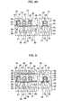
- element regions are defined by forming, for example, STI (Shallow Trench Isolation) element isolation structures 2 as element isolation structures on a silicon semiconductor substrate 1 (in the example in the drawing, the left is a memory cell region 11 and the right is a peripheral circuit (logic) region 12), and gate electrode structures 13, each of which is formed to have a source/drain 4 on the semiconductor substrate 1 of both sides thereof, are formed on wells 3a and 3b of the regions 11 and 12.
- STI Shallow Trench Isolation
- the gate electrode structure 13 is structured in a manner that a gate electrode 6 and its cap insulating film 7 are pattern-formed on the semiconductor substrate 1 with a gate insulating film 5 therebetween, a silicon nitride film 9 is further formed to cover the gate electrode 6 and the cap insulating film 7 in the memory cell region while side walls 8 are further formed on the sides of the gate electrode 6 and the cap insulating film 7 in the peripheral circuit region 12, and a silicon nitride film 14 as an etching stopper is formed in each of the regions 11 and 12. Moreover, in the peripheral circuit region 12, a Co silicide film 15 for lowering the resistance is formed on the source/drain.
- the present invention is mainly directed to a semiconductor device in which a plurality of the gate electrode structures 13 are formed in the memory cell region 11 and the gate length is 110 nm ⁇ 15 nm or shorter (130 nm or shorter in a design rule) or an aspect ratio of an area between adjacent gate electrode structures 13 (a ratio of the height of the gate electrode structure 13 to the distance between the gate electrode structures 13) is 6 or higher.
- an interlayer insulating film 10 is formed to cover the whole regions 11 and 12 and to fill the area between the adjacent gate electrode structures 13 in the memory cell region 11.
- the area between the gate electrode structures means a gap between the silicon nitride films 14 of the adjacent gate electrode structures 13 in this example.
- a silicon oxide film containing a conductive impurity, a PSG (HDP-PSG: Phospho Silicate Glass) film in this case is formed as the interlayer insulating film 10 to bury the gate electrode structures 13 at the film-formation temperature of 650°C or lower through the use of a high-density plasma CVD (HDP-CVD) method in order to respond to a demand for securing ability of filling the area between the gate electrode structures 13, which is resulted from the further shortened gate length and distance between the gate electrode structures 13, while responding to a demand for controlling the temperature.
- HDP-CVD high-density plasma CVD
- the PSG film, which contains phosphorus as the interlayer insulating film 10
- an etching rate of the interlayer insulating film 10 increases, which can contribute to the improvement in workability when a contact hole is formed. Furthermore, in this case, since phosphorus has a gettering effect of mobile ions, metallic contamination which tends to occur in a manufacturing process is prevented by gettering, which can improve the reliability of the device.
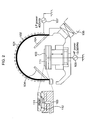
- This HDP-CVD apparatus has, in a ceramic chamber 101 structured by winding a coil 102, an electrostatic chuck 103 on which a semiconductor substrate 111 is placed and fixed, a supply tube 104 for supplying a growth gas, and a turbo pump 105 for adjusting the inside of the chamber 101 in a desirable vacuum state.
- a high-frequency power source 106 of, for example, 13.56 MHz and a low-frequency power source 107 of, for example, 400 kHz are provided to the electrostatic chuck 103 and the chamber 101, respectively.
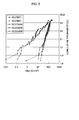
- V th which is an initial characteristic of a transistor
- Fig. 3A shows a case without an antenna while Fig. 3B shows a case with an antenna ratio of 250.
- the HDP-PSG film shown by BUC: Bias UnClamped in the chart.
- 7K has film thickness of 700 nm and 2K has film thickness of 200 nm
- a TEOS-O 3 NSG (Non-doped-CVD - Silicate glass) film shown by WJ in the chart
- threshold voltages V th of both films are similar and influence of plasma damage is not seen.
- the inventor of the present invention has assumed that the degradation in the Qbd characteristic is attributed to the temperature condition in HDP treatment, and has considered that it is necessary to further lower the film-formation temperature to improve the Qbd characteristic. Therefore, as a specific preferable method to lower the film-formation temperature, a BC (Bias Clamped) process was applied, that is, as shown in Fig. 2, the HDP-PSG film was formed by clamping the semiconductor substrate 111 in the electrostatic chuck 103 and cooling it while letting He gas flow toward a rear surface of the substrate by a He supply mechanism 112 which is provided in the electrostatic chuck 103. In this case, the film-formation temperature can be lowered to approximately 450°C.
- the HDP-PSG film (shown by BC2250: Bias Clamped; HF2250 W in the chart) formed at approximately 460°C under the film-formation condition described above has the equal threshold voltage V th to that of the TEOS-O 3 NSG film (WJ) as shown in Fig. 3A, substantial improvement is seen in its Qbd characteristic compared with the HDP-PSG film (BUC) which has been formed under the temperature condition of 650°C as shown in Fig. 4.
- the Qbd characteristic can be improved to be equal to that of the TEOS-O 3 NSG film (WJ).
- the inventor of the present invention has intended to increase the mean free path of gas molecules in a film-formation chamber in order to recover filling ability degraded by the lowering of the film-formation temperature, and has thought of lowering pressure in forming the HDP-PSG film. Specifically, when a film-formation pressure was set at approximately 2.7 ⁇ 10 2 Pa (2.0 mTorr), although the film-formation pressure had been set at approximately 4.7 ⁇ 10 2 Pa (3.5 mTorr) in Fig. 6B, while maintaining other conditions at equal values, it has been found that the slit voids do not occur and high filling ability is obtained as shown in an SEM photograph in Fig. 7. Accordingly, by applying the present invention, it becomes possible to attain excellent filling ability for the semiconductor device whose gate length is 110 nm or shorter (or the aspect ratio of the area between gate electrode structures thereof is 6 or higher) without concern for plasma damage.
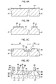
- Fig. 8A to Fig. 8K are schematic sectional views showing the method for manufacturing the DRAM and logic combined type device according to the embodiment in the order of steps.
- element regions are defined by forming element isolation structures on a semiconductor substrate.
- a thermal oxide film 22 and a thermal nitride film 23 are sequentially formed on a surface of a silicon semiconductor substrate 21 in film thickness of approximately 5 nm and approximately 100 nm, respectively.
- the thermal nitride film 23 is patterned through the use of a photoresist so that only the thermal nitride films 23 in parts to be the element regions remain. Then, after the photoresist is removed by ashing, the thermal oxide film 22 and the semiconductor substrate 21 are etched with the patterned thermal nitride films 23 as hard masks so that trenches 24 having depth of approximately 300 nm are formed in parts to be the element isolation regions of the semiconductor substrate 21.
- a silicon oxide film 26 is formed in film thickness of approximately 700 nm by a high-density plasma CVD method so that the trenches 24 are filled.
- the HDP silicon oxide film 26 is polished and flattened with the thermal nitride films 23 as stoppers by a CMP (Chemical Mechanical Polishing) method. Then, the thermal nitride films 23 are removed through the use of phosphoric acid.
- STI element isolation structures 51 in which the trenches 24 formed in the element isolating regions of the semiconductor substrate 21 are charged with the HDP silicon oxide films 26 are formed.
- the left is a memory cell region 52 and the right is a peripheral circuit (logic) region 53 in the drawing.
- n-well 30 is formed in a part to be a p-channel transistor and a p-well 31 is further formed in the part to be the n-channel transistor.
- a polycrystalline silicon film and a silicon nitride film are sequentially formed in film thickness of approximately 160 nm and 150 nm, respectively, by a CVD method.
- the silicon nitride film, the polycrystalline silicon film, and the silicon oxide film are patterned through the use of a photoresist to form gate electrodes 28 formed on the semiconductor substrate 21 with gate insulating films 27 therebetween and having cap insulating films 29 on upper surfaces thereof.
- the gate length of the gate electrode 28 in a design rule is supposed to be 130 nm and the actual gate length is controlled to be approximately 110 nm ⁇ 15 nm.
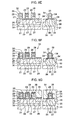
- a silicon nitride film 32 is entirely formed in film thickness of approximately 60 nm by a thermal CVD method, and the silicon nitride film 32 in the peripheral circuit region 53 is anisotropically etched (etchback) while masking the memory cell region 52 so that sidewalls 54 are formed on the sides of the gate electrode 28 and the cap insulating film 29 in the peripheral circuit region 53.
- an impurity is ion-implanted in each of the regions 52 and 53.
- the cap insulating films 29 in the memory cell region 52 and the cap insulating film 29 and the sidewalls 54 in the peripheral circuit region 53 work as masks, respectively, and sources/drains 33 are formed on a surface layer of the semiconductor substrate 21 on both sides of the gate electrodes 28.
- the impurity arsenic (As) is used for the part to be the n-channel transistor and boron (B) is used for the part to be the p-channel transistor.
- a Co film is formed only in the peripheral circuit region 53 by a sputtering method while masking the memory cell region 52, and is thermally treated in a rapid anneal (RTA: Rapid Thermal Anneal) method so that the source/drain 33 and the Co film are made to react, thereby forming Co silicide films 34 on the source/drain 33.
- RTA Rapid Thermal Anneal
- This RTA treatment may be performed in an atmosphere with N 2 of 10 (l/min) at 500°C for 30 seconds.
- a silicon nitride film 35 which functions as an etching stopper in forming contact holes, which will be described later, is formed all over the regions 52 and 53 in film thickness of approximately 25 nm.
- the temperature may be set at 400°C, and a parallel plane plasma CVD apparatus is used with SiH 4 /NH 3 gas as a growth gas. Further, in order to prevent local overetching due to ununiformity of the film thickness, it is essential to secure the film thickness of the silicon nitride film 35 of approximately 25 nm.
- a structure composed of the gate electrode 28, the cap .insulating film 29, and the silicon nitride films 32 and 35 is defined as a gate electrode structure 55.
- the distance between the gate electrode structures 55 that is, the distance between the silicon nitride films 35 in a gap between adjacent gate electrode structures 55, is approximately 50 nm and the height of the gate electrode structure 55 is approximately 300 nm, which causes an aspect ratio of the gap to be approximately 6.
- a structure composed of the gate electrode 28, the cap insulating film 29, the sidewalls 54, and the silicon nitride film 35 is defined as a gate electrode structure 56.
- an HDP-PSG film 36 is entirely deposited as an interlayer insulating film in a manner of filling the gap.
- the LF(400 kHz)/HF(13.56 MHz) are set at 3100/2250 W
- phosphorus concentration is set at 5 wt %
- the film-formation temperature is set at 600°C to 650°C
- the film is formed without clamping the semiconductor substrate 21 by the electrostatic chuck.
- an upper surface of the HDP-PSG film 36 is flattened by the CMP method.
- contact holes 57 which expose surfaces of the sources/drains 33 between the gate electrode structures 55, are formed in the HDP-PSG film 36 in the memory cell region 52 by a SAC (Self Align Contact) method.
- each of the contact holes 57 is formed in a design rule such that its hole diameter is larger than the distance between the gate electrode structures 55 (gap distance), but it is controlled to the gap distance by the silicon nitride films 35, which work as etching stoppers, and formed to have the hole diameter of the gap distance in a self-aligning manner in the area between the gate electrode structures 55.
- a DASI (Doped Amorphous Silicon) film is formed in a manner of filling the contact holes 57, and the DASI film is polished by the CMP method with the HDP-PSG film 36 as a stopper so that DASI plugs 37 in which the contact holes 57 are charged with DASI are formed.
- DASI Doped Amorphous Silicon
- a silicon oxide film 58 is formed on the HDP-PSG film 36 by a plasma CVD method or the thermal CVD method, a glue layer consisting of Ti/TiN is formed by the CVD method, and a tungsten (W) film is formed by the CVD method. Thereafter, the W film is patterned through the use of a photoresist to form bit lines 38. Then, a USG film 59 is formed in a manner of burying the bit lines 38 by the HDP-CVD method, and its upper surface is flattened by the CMP method or the like.
- memory capacitors are formed in the memory cell region 52.
- via holes 61 which communicate with the DASI plugs 37 are formed in the USG film 59 and the silicon oxide film 58, a DASI film is formed on the USG film 59 in a manner of filling the via holes 61, and the DASI film is patterned so that storage node electrodes 62 are formed. Thereafter, a dielectric film 63 and a DASI film are sequentially formed to cover the storage node electrodes 62, and the DASI film and the dielectric film 63 are patterned so that a cell plate electrode 64 covering the storage node electrodes 62 via the dielectric film 63 is formed.
- memory capacitors 60 in which the storage node electrodes 62 and the cell plate electrode 64 are capacitively coupled via the dielectric film 63 are formed.
- a USG film 65 is formed to cover the memory capacitors 60 by the HDP-CVD method, and its surface is flattened by the CMP method or the like.
- a via hole 71 which exposes a surface of the cell plate electrode 64 and a contact hole 72 which exposes a surface of the Co silicide film 34 are simultaneously formed.
- the via hole 71 is formed in the USG film 65.
- the contact hole 72 is formed in the USG film 65, the USG film 59, the silicon oxide film 58, and the HDP-PSG film 36.
- the via hole 71 is formed and the contact hole 72 is opened up to the silicon oxide film 58.
- the HDP-PSG film 36 is etched so that the contact hole 72 is formed.
- the cell plate electrode 64 works as an etching stopper.
- a via hole 73 which exposes a surface of the bit line 38 is formed in the USG films 65 and 59.
- a W film is formed by the CVD method or the like in a manner of filling the via holes 71 and 73 and the contact hole 72, and a surface of the W film is polished by the CMP method so that W plugs 81, 83, and 82 in which the via holes 71 and 73 and the contact hole 72 are buried with W are formed.
- a glue layer consisting of Ti/TiN is formed on the USG film 65 by the CVD method, an aluminum (Al) film is formed by the sputtering method, the Al film is patterned to form Al wirings 84 which are connected with the W plugs 81, 82, and 83 respectively, and a USG film 66 is formed by the plasma CVD method in a manner of burying the Al wirings 84.
- the present invention is not limited to the above-described embodiment but preferably applied to a logic device or other various semiconductor devices requiring finer gate electrodes, other than the DRAM and logic combined type device.
Landscapes
- Engineering & Computer Science (AREA)
- Manufacturing & Machinery (AREA)
- Semiconductor Memories (AREA)
- Internal Circuitry In Semiconductor Integrated Circuit Devices (AREA)
- Insulated Gate Type Field-Effect Transistor (AREA)
- Metal-Oxide And Bipolar Metal-Oxide Semiconductor Integrated Circuits (AREA)
- Formation Of Insulating Films (AREA)
- Electrodes Of Semiconductors (AREA)
Abstract
Description
Claims (56)
- A method for manufacturing a semiconductor device comprising the steps of:forming at least one gate electrode structure on a semiconductor substrate with a gate insulating film therebetween so that gate length thereof is 110 nm or shorter; andforming a silicon oxide film containing a conductive impurity at film-formation temperature of 650°C or lower by a high-density plasma CVD method so that difference in a surface level due to said gate electrode structure is lessened.
- The method for manufacturing the semiconductor device according to claim 1,
wherein, in forming said gate electrode structure, a design rule of said gate length is set at 130 nm or shorter. - The method for manufacturing the semiconductor device according to claim 1,
wherein said silicon oxide film is a PSG film. - The method for manufacturing the semiconductor device according to claim 2,
wherein said silicon oxide film is a PSG film. - The method for manufacturing the semiconductor device according to claim 1,
wherein said gate electrode structure is formed in a manner in which a pattern-formed gate electrode is covered with an insulating film, and said silicon oxide film is formed in a manner of burying said gate electrode structure. - The method for manufacturing the semiconductor device according to claim 2,
wherein said gate electrode structure is formed in a manner in which a pattern-formed gate electrode is covered with an insulating film, and said silicon oxide film is formed in a manner of burying said gate electrode structure. - The method for manufacturing the semiconductor device according to claim 3,
wherein said gate electrode structure is formed in a manner in which a pattern-formed gate electrode is covered with an insulating film, and said silicon oxide film is formed in a manner of burying said gate electrode structure. - The method for manufacturing the semiconductor device according to claim 4,
wherein said gate electrode structure is formed in a manner in which a pattern-formed gate electrode is covered with an insulating film, and said silicon oxide film is formed in a manner of burying said gate electrode structure. - The method for manufacturing the semiconductor device according to claim 1,
wherein an aspect ratio of an area between adjacent gate electrode structures is 6 or higher. - The method for manufacturing the semiconductor device according to claim 2,
wherein an aspect ratio of an area between adjacent gate electrode structures is 6 or higher. - The method for manufacturing the semiconductor device according to claim 3,
wherein an aspect ratio of an area between adjacent gate electrode structures is 6 or higher. - The method for manufacturing the semiconductor device according to claim 4,
wherein an aspect ratio of an area between adjacent gate electrode structures is 6 or higher. - The method for manufacturing the semiconductor device according to claim 5,
wherein an aspect ratio of an area between adjacent gate electrode structures is 6 or higher. - The method for manufacturing the semiconductor device according to claim 6,
wherein an aspect ratio of an area between adjacent gate electrode structures is 6 or higher. - The method for manufacturing the semiconductor device according to claim 7,
wherein an aspect ratio of an area between adjacent gate electrode structures is 6 or higher. - The method for manufacturing the semiconductor device according to claim 8,
wherein an aspect ratio of an area between adjacent gate electrode structures is 6 or higher. - The method for manufacturing the semiconductor device according to claim 1,
wherein, in forming said silicon oxide film, a growth gas containing He gas is used. - The method for manufacturing the semiconductor device according to claim 2,
wherein, in forming said silicon oxide film, a growth gas containing He gas is used. - The method for manufacturing the semiconductor device according to claim 3,
wherein, in forming said silicon oxide film, a growth gas containing He gas is used. - The method for manufacturing the semiconductor device according to claim 4,
wherein, in forming said silicon oxide film, a growth gas containing He gas is used. - The method for manufacturing the semiconductor device according to claim 5,
wherein, in forming said silicon oxide film, a growth gas containing He gas is used. - The method for manufacturing the semiconductor device according to claim 6,
wherein, in forming said silicon oxide film, a growth gas containing He gas is used. - The method for manufacturing the semiconductor device according to claim 7,
wherein, in forming said silicon oxide film, a growth gas containing He gas is used. - The method for manufacturing the semiconductor device according to claim 8,
wherein, in forming said silicon oxide film, a growth gas containing He gas is used. - The method for manufacturing the semiconductor device according to claim 9,
wherein, in forming said silicon oxide film, a growth gas containing He gas is used. - The method for manufacturing the semiconductor device according to claim 10,
wherein, in forming said silicon oxide film, a growth gas containing He gas is used. - The method for manufacturing the semiconductor device according to claim 11,
wherein, in forming said silicon oxide film, a growth gas containing He gas is used. - The method for manufacturing the semiconductor device according to claim 12,
wherein, in forming said silicon oxide film, a growth gas containing He gas is used. - The method for manufacturing the semiconductor device according to claim 13,
wherein, in forming said silicon oxide film, a growth gas containing He gas is used. - The method for manufacturing the semiconductor device according to claim 14,
wherein, in forming said silicon oxide film, a growth gas containing He gas is used. - The method for manufacturing the semiconductor device according to claim 15,
wherein, in forming said silicon oxide film, a growth gas containing He gas is used. - The method for manufacturing the semiconductor device according to claim 16,
wherein, in forming said silicon oxide film, a growth gas containing He gas is used. - The method for manufacturing the semiconductor device according to claim 1,
wherein, the step of forming said silicon oxide film comprises the step of letting He gas flow toward a rear face of said semiconductor substrate, thereby controlling said film-formation temperature. - The method for manufacturing the semiconductor device according to claim 1,
wherein, in forming said silicon oxide film, film-formation pressure is set at 0.47 Pa or lower. - A method for manufacturing a semiconductor device comprising the steps of:forming a plurality of gate electrode structures on a semiconductor substrate with a gate insulating film therebetween so that an aspect ratio of a part between adjacent gate electrode structures is 6 or higher; andforming a silicon oxide film containing a conductive impurity at film-formation temperature of 650°C or lower by a high-density plasma CVD method in a manner of filling said part between said adjacent gate electrode structures and burying said gate electrode structures.
- The method for manufacturing the semiconductor device according to claim 35,
wherein said silicon oxide film is a PSG film. - The method for manufacturing the semiconductor device according to claim 35,
wherein said gate electrode structures are formed in a manner in which pattern-formed gate electrodes are covered with an insulating film, and said silicon oxide film is formed in a manner of burying said gate electrode structures. - The method for manufacturing the semiconductor device according to claim 36,
wherein said gate electrode structures are formed in a manner in which pattern-formed gate electrodes are covered with an insulating film, and said silicon oxide film is formed in a manner of burying said gate electrode structures. - The method for manufacturing the semiconductor device according to claim 35,
wherein, in forming said silicon oxide film, a growth gas containing He gas is used. - The method for manufacturing the semiconductor device according to claim 36,
wherein, in forming said silicon oxide film, a growth gas containing He gas is used. - The method for manufacturing the semiconductor device according to claim 37,
wherein, in forming said silicon oxide film, a growth gas containing He gas is used. - The method for manufacturing the semiconductor device according to claim 38,
wherein, in forming said silicon oxide film, a growth gas containing He gas is used. - The method for manufacturing the semiconductor device according to claim 35,
wherein, the step of forming said silicon oxide film comprises the step of letting He gas flow toward a rear face of said semiconductor substrate, thereby controlling said film-formation temperature. - The method for manufacturing the semiconductor device according to claim 35,
wherein, in forming said silicon oxide film, film-formation pressure is set at 0.47 Pa or lower. - A semiconductor device comprising:at least one gate electrode structure formed on a semiconductor substrate with a gate insulating film therebetween and having gate length of 110 nm or shorter; anda silicon oxide film containing a conductive impurity formed by a high-density plasma CVD method so that difference in a surface level due to said gate electrode structure is lessened.
- The semiconductor device according to claim 45,
wherein said silicon oxide film is a PSG film. - The semiconductor device according to claim 45,
wherein said gate electrode structure comprises a gate electrode, and an insulating film which covers said gate electrode. - The semiconductor device according to claim 46,
wherein said gate electrode structure comprises a gate electrode, and an insulating film which covers said gate electrode. - The semiconductor device according to claim 45,
wherein an aspect ratio of a part between adjacent gate electrode structures is 6 or higher. - The semiconductor device according to claim 46,
wherein an aspect ratio of a part between adjacent gate electrode structures is 6 or higher. - The semiconductor device according to claim 47,
wherein an aspect ratio of a part between adjacent gate electrode structures is 6 or higher. - The semiconductor device according to claim 48,
wherein an aspect ratio of a part between adjacent gate electrode structures is 6 or higher. - A semiconductor device comprising:a plurality of gate electrode structures formed on a semiconductor substrate with a gate insulating film therebetween so that an aspect ratio of a part between adjacent gate electrode structures is 6 or higher; anda silicon oxide film containing a conductive impurity formed by a high-density plasma CVD method in a manner of filling the part between said adjacent gate electrode structures and burying said gate electrode structures.
- The semiconductor device according to claim 53,
wherein said silicon oxide film is a PSG film. - The semiconductor device according to claim 53,
wherein said gate electrode structures are formed in a manner in which gate electrodes are covered with an insulating film. - The semiconductor device according to claim 54,
wherein said gate electrode structures are formed in a manner in which gate electrodes are covered with an insulating film.
Applications Claiming Priority (2)
| Application Number | Priority Date | Filing Date | Title |
|---|---|---|---|
| JP2002086439 | 2002-03-26 | ||
| JP2002086439A JP3975099B2 (en) | 2002-03-26 | 2002-03-26 | Manufacturing method of semiconductor device |
Publications (2)
| Publication Number | Publication Date |
|---|---|
| EP1351287A2 true EP1351287A2 (en) | 2003-10-08 |
| EP1351287A3 EP1351287A3 (en) | 2009-03-11 |
Family
ID=28035840
Family Applications (1)
| Application Number | Title | Priority Date | Filing Date |
|---|---|---|---|
| EP02025620A Withdrawn EP1351287A3 (en) | 2002-03-26 | 2002-11-19 | Semiconductor device and method for manufacturing the same |
Country Status (6)
| Country | Link |
|---|---|
| US (2) | US7320917B2 (en) |
| EP (1) | EP1351287A3 (en) |
| JP (1) | JP3975099B2 (en) |
| KR (1) | KR20030077929A (en) |
| CN (1) | CN1310304C (en) |
| TW (1) | TW564475B (en) |
Cited By (2)
| Publication number | Priority date | Publication date | Assignee | Title |
|---|---|---|---|---|
| DE102006060770A1 (en) * | 2006-12-21 | 2008-07-03 | Qimonda Ag | Production method for an integrated semiconductor structure and corresponding semiconductor structure |
| CN102945808B (en) * | 2012-11-30 | 2017-06-23 | 上海华虹宏力半导体制造有限公司 | Groove type MOS transistor manufacture method |
Families Citing this family (11)
| Publication number | Priority date | Publication date | Assignee | Title |
|---|---|---|---|---|
| JP3975099B2 (en) * | 2002-03-26 | 2007-09-12 | 富士通株式会社 | Manufacturing method of semiconductor device |
| KR100610436B1 (en) * | 2003-12-23 | 2006-08-08 | 주식회사 하이닉스반도체 | Method for suppressing deterioration of gate oxide film |
| JP2005203471A (en) * | 2004-01-14 | 2005-07-28 | Nec Electronics Corp | Method of manufacturing semiconductor device |
| JP2005327848A (en) * | 2004-05-13 | 2005-11-24 | Toshiba Corp | Semiconductor device and manufacturing method thereof |
| US7329586B2 (en) * | 2005-06-24 | 2008-02-12 | Applied Materials, Inc. | Gapfill using deposition-etch sequence |
| US7670938B2 (en) * | 2006-05-02 | 2010-03-02 | GlobalFoundries, Inc. | Methods of forming contact openings |
| US8435898B2 (en) * | 2007-04-05 | 2013-05-07 | Freescale Semiconductor, Inc. | First inter-layer dielectric stack for non-volatile memory |
| KR101195268B1 (en) * | 2011-02-14 | 2012-11-14 | 에스케이하이닉스 주식회사 | Semiconductor device comprising capacitor and double-layered metal contact and method for fabricating the same |
| KR101581595B1 (en) * | 2011-06-24 | 2015-12-30 | 도오꾜오까고오교 가부시끼가이샤 | Method of manufacturing multilayer body, method of processing substrate, and multilayer body |
| KR102314778B1 (en) * | 2015-08-21 | 2021-10-21 | 삼성전자주식회사 | Semiconductor device |
| CN112151450B (en) | 2019-06-26 | 2023-08-08 | 联华电子股份有限公司 | Semiconductor structures and methods of forming them |
Family Cites Families (43)
| Publication number | Priority date | Publication date | Assignee | Title |
|---|---|---|---|---|
| US355547A (en) * | 1887-01-04 | mebcee | ||
| ATE145495T1 (en) * | 1990-05-31 | 1996-12-15 | Canon Kk | METHOD FOR WIRING A SEMICONDUCTOR CIRCUIT |
| JP2913817B2 (en) * | 1990-10-30 | 1999-06-28 | 日本電気株式会社 | Method for manufacturing semiconductor memory |
| JPH08115911A (en) | 1994-08-25 | 1996-05-07 | Sony Corp | Method for manufacturing semiconductor device |
| US6013584A (en) | 1997-02-19 | 2000-01-11 | Applied Materials, Inc. | Methods and apparatus for forming HDP-CVD PSG film used for advanced pre-metal dielectric layer applications |
| US6268297B1 (en) | 1997-11-26 | 2001-07-31 | Texas Instruments Incorporated | Self-planarizing low-temperature doped-silicate-glass process capable of gap-filling narrow spaces |
| KR100249025B1 (en) * | 1998-03-06 | 2000-03-15 | 김영환 | Semiconductor element isolating method |
| JP2000082750A (en) * | 1998-07-10 | 2000-03-21 | Oki Electric Ind Co Ltd | Method for manufacturing semiconductor device |
| JP3267257B2 (en) | 1998-12-16 | 2002-03-18 | 日本電気株式会社 | Method for manufacturing semiconductor device |
| CN1301537C (en) | 1999-04-16 | 2007-02-21 | 国际商业机器公司 | Low temperature reflux dielectric-boron phosphor-silicon fluorine glass |
| KR100308619B1 (en) * | 1999-08-24 | 2001-11-01 | 윤종용 | Method of forming a self-aligned contact pad for a semiconductor device |
| JP3393602B2 (en) * | 2000-01-13 | 2003-04-07 | 松下電器産業株式会社 | Semiconductor device |
| US6355581B1 (en) * | 2000-02-23 | 2002-03-12 | Chartered Semiconductor Manufacturing Ltd. | Gas-phase additives for an enhancement of lateral etch component during high density plasma film deposition to improve film gap-fill capability |
| JP3519662B2 (en) * | 2000-03-14 | 2004-04-19 | 松下電器産業株式会社 | Semiconductor device and manufacturing method thereof |
| JP5116189B2 (en) | 2000-07-18 | 2013-01-09 | アプライド マテリアルズ インコーポレイテッド | Method and apparatus for manufacturing semiconductor device |
| JP2002076332A (en) * | 2000-08-24 | 2002-03-15 | Hitachi Ltd | Insulated gate field effect transistor and method of manufacturing the same |
| US6613697B1 (en) * | 2001-06-26 | 2003-09-02 | Special Materials Research And Technology, Inc. | Low metallic impurity SiO based thin film dielectrics on semiconductor substrates using a room temperature wet chemical growth process, method and applications thereof |
| JP2003037264A (en) * | 2001-07-24 | 2003-02-07 | Toshiba Corp | Semiconductor device and method of manufacturing the same |
| JP4628644B2 (en) * | 2001-10-04 | 2011-02-09 | 富士通セミコンダクター株式会社 | Manufacturing method of semiconductor device |
| JP4212018B2 (en) * | 2001-11-30 | 2009-01-21 | 富士通マイクロエレクトロニクス株式会社 | Manufacturing method of semiconductor device |
| JP3951743B2 (en) * | 2002-02-28 | 2007-08-01 | 松下電器産業株式会社 | Semiconductor device and manufacturing method thereof |
| JP4134575B2 (en) * | 2002-02-28 | 2008-08-20 | 松下電器産業株式会社 | Semiconductor device and manufacturing method thereof |
| JP4173672B2 (en) * | 2002-03-19 | 2008-10-29 | 株式会社ルネサステクノロジ | Semiconductor device and manufacturing method thereof |
| JP3975099B2 (en) * | 2002-03-26 | 2007-09-12 | 富士通株式会社 | Manufacturing method of semiconductor device |
| US6462375B1 (en) * | 2002-04-01 | 2002-10-08 | Silicon Based Technology Corp. | Scalable dual-bit flash memory cell and its contactless flash memory array |
| US6690058B2 (en) * | 2002-04-10 | 2004-02-10 | Ching-Yuan Wu | Self-aligned multi-bit flash memory cell and its contactless flash memory array |
| US6528843B1 (en) * | 2002-05-03 | 2003-03-04 | Silicon Based Technology Corp. | Self-aligned split-gate flash memory cell having a single-side tip-shaped floating-gate structure and its contactless flash memory arrays |
| US6525369B1 (en) * | 2002-05-13 | 2003-02-25 | Ching-Yuan Wu | Self-aligned split-gate flash memory cell and its contactless flash memory arrays |
| US6531734B1 (en) * | 2002-05-24 | 2003-03-11 | Silicon Based Technology Corp. | Self-aligned split-gate flash memory cell having an integrated source-side erase structure and its contactless flash memory arrays |
| JP2004214607A (en) * | 2002-12-19 | 2004-07-29 | Renesas Technology Corp | Semiconductor device and manufacturing method thereof |
| US6710396B1 (en) * | 2003-01-24 | 2004-03-23 | Silicon-Based Technology Corp. | Self-aligned split-gate flash cell structure and its contactless flash memory arrays |
| JP4331690B2 (en) * | 2003-04-30 | 2009-09-16 | 富士通マイクロエレクトロニクス株式会社 | Manufacturing method of semiconductor device |
| WO2004112139A1 (en) * | 2003-06-10 | 2004-12-23 | Fujitsu Limited | Semiconductor device and its manufacturing method |
| JP4837902B2 (en) * | 2004-06-24 | 2011-12-14 | 富士通セミコンダクター株式会社 | Semiconductor device |
| JP4444027B2 (en) * | 2004-07-08 | 2010-03-31 | 富士通マイクロエレクトロニクス株式会社 | N-channel MOS transistor and CMOS integrated circuit device |
| JP4343798B2 (en) * | 2004-08-26 | 2009-10-14 | 富士通マイクロエレクトロニクス株式会社 | Manufacturing method of semiconductor device |
| US20060157776A1 (en) * | 2005-01-20 | 2006-07-20 | Cheng-Hung Chang | System and method for contact module processing |
| JP4185057B2 (en) * | 2005-01-28 | 2008-11-19 | 富士通株式会社 | Manufacturing method of semiconductor device |
| JP2006210828A (en) * | 2005-01-31 | 2006-08-10 | Fujitsu Ltd | Semiconductor device and manufacturing method thereof |
| JP4361886B2 (en) * | 2005-02-24 | 2009-11-11 | 富士通マイクロエレクトロニクス株式会社 | Semiconductor integrated circuit device and manufacturing method thereof |
| JP4515305B2 (en) * | 2005-03-29 | 2010-07-28 | 富士通セミコンダクター株式会社 | P-channel MOS transistor and method for manufacturing the same, and method for manufacturing a semiconductor integrated circuit device |
| KR100695868B1 (en) * | 2005-06-23 | 2007-03-19 | 삼성전자주식회사 | A device isolation film, a method of manufacturing the same, a semiconductor device having the same and a method of manufacturing the same |
| TWI338329B (en) * | 2005-07-11 | 2011-03-01 | Fujitsu Semiconductor Ltd | Manufacture of semiconductor device with cmp |
-
2002
- 2002-03-26 JP JP2002086439A patent/JP3975099B2/en not_active Expired - Fee Related
- 2002-10-21 TW TW091124238A patent/TW564475B/en not_active IP Right Cessation
- 2002-10-22 US US10/274,876 patent/US7320917B2/en not_active Expired - Lifetime
- 2002-10-29 KR KR1020020066076A patent/KR20030077929A/en not_active Ceased
- 2002-11-19 EP EP02025620A patent/EP1351287A3/en not_active Withdrawn
- 2002-11-21 CN CNB021513783A patent/CN1310304C/en not_active Expired - Fee Related
-
2007
- 2007-02-22 US US11/709,262 patent/US20070145494A1/en not_active Abandoned
Cited By (2)
| Publication number | Priority date | Publication date | Assignee | Title |
|---|---|---|---|---|
| DE102006060770A1 (en) * | 2006-12-21 | 2008-07-03 | Qimonda Ag | Production method for an integrated semiconductor structure and corresponding semiconductor structure |
| CN102945808B (en) * | 2012-11-30 | 2017-06-23 | 上海华虹宏力半导体制造有限公司 | Groove type MOS transistor manufacture method |
Also Published As
| Publication number | Publication date |
|---|---|
| CN1310304C (en) | 2007-04-11 |
| CN1447390A (en) | 2003-10-08 |
| JP3975099B2 (en) | 2007-09-12 |
| US7320917B2 (en) | 2008-01-22 |
| TW564475B (en) | 2003-12-01 |
| KR20030077929A (en) | 2003-10-04 |
| JP2003282702A (en) | 2003-10-03 |
| US20030183898A1 (en) | 2003-10-02 |
| US20070145494A1 (en) | 2007-06-28 |
| EP1351287A3 (en) | 2009-03-11 |
Similar Documents
| Publication | Publication Date | Title |
|---|---|---|
| US20070145494A1 (en) | Semiconductor device and method for manufacturing the same | |
| US7745303B2 (en) | Method of manufacturing a semiconductor device and the semiconductor device | |
| US6900492B2 (en) | Integrated circuit device with P-type gate memory cell having pedestal contact plug and peripheral circuit | |
| US8686535B2 (en) | Trench isolation implantation | |
| US6414364B2 (en) | Isolation structure and process therefor | |
| US6410423B1 (en) | Semiconductor device and manufacturing method thereof | |
| US6255160B1 (en) | Cell design and process for making dynamic random access memory (DRAM) having one or more Gigabits of memory cells | |
| KR100719015B1 (en) | A method of manufacturing a semiconductor integrated circuit device | |
| KR100360396B1 (en) | Method for forming contact structure of semiconductor device | |
| US20030216030A1 (en) | Method for fabricating contact plug with low contact resistance | |
| JPH1027889A (en) | Semiconductor device and manufacturing method thereof | |
| JPH11243180A (en) | Method for manufacturing semiconductor device | |
| US6680511B2 (en) | Integrated circuit devices providing improved short prevention | |
| US20020190316A1 (en) | Semiconductor device with borderless contact structure and method of manufacturing the same | |
| US20030215997A1 (en) | Method of manufacturing semiconductor device | |
| JP2001077189A (en) | Method for manufacturing semiconductor device | |
| KR101082090B1 (en) | Method for fabricating trench isolation in semiconductor device | |
| US6251769B1 (en) | Method of manufacturing contact pad | |
| KR20060074719A (en) | Method of manufacturing semiconductor device using tungsten process | |
| JP2000174125A (en) | Semiconductor device and manufacturing method thereof | |
| KR20020078427A (en) | method of forming inter layer dielectric semiconductor device |
Legal Events
| Date | Code | Title | Description |
|---|---|---|---|
| PUAI | Public reference made under article 153(3) epc to a published international application that has entered the european phase |
Free format text: ORIGINAL CODE: 0009012 |
|
| AK | Designated contracting states |
Kind code of ref document: A2 Designated state(s): AT BE BG CH CY CZ DE DK EE ES FI FR GB GR IE IT LI LU MC NL PT SE SK TR |
|
| AX | Request for extension of the european patent |
Extension state: AL LT LV MK RO SI |
|
| RAP1 | Party data changed (applicant data changed or rights of an application transferred) |
Owner name: FUJITSU MICROELECTRONICS LIMITED |
|
| PUAL | Search report despatched |
Free format text: ORIGINAL CODE: 0009013 |
|
| AK | Designated contracting states |
Kind code of ref document: A3 Designated state(s): AT BE BG CH CY CZ DE DK EE ES FI FR GB GR IE IT LI LU MC NL PT SE SK TR |
|
| AX | Request for extension of the european patent |
Extension state: AL LT LV MK RO SI |
|
| RIC1 | Information provided on ipc code assigned before grant |
Ipc: H01L 21/316 20060101ALI20090205BHEP Ipc: H01L 21/768 20060101AFI20030712BHEP |
|
| AKX | Designation fees paid | ||
| STAA | Information on the status of an ep patent application or granted ep patent |
Free format text: STATUS: THE APPLICATION IS DEEMED TO BE WITHDRAWN |
|
| 18D | Application deemed to be withdrawn |
Effective date: 20090912 |
|
| REG | Reference to a national code |
Ref country code: DE Ref legal event code: 8566 |