EP1351254A2 - An integrated fuse with regions of different doping within the fuse neck - Google Patents
An integrated fuse with regions of different doping within the fuse neck Download PDFInfo
- Publication number
- EP1351254A2 EP1351254A2 EP03007698A EP03007698A EP1351254A2 EP 1351254 A2 EP1351254 A2 EP 1351254A2 EP 03007698 A EP03007698 A EP 03007698A EP 03007698 A EP03007698 A EP 03007698A EP 1351254 A2 EP1351254 A2 EP 1351254A2
- Authority
- EP
- European Patent Office
- Prior art keywords
- fuse
- region
- type
- dopant
- regions
- Prior art date
- Legal status (The legal status is an assumption and is not a legal conclusion. Google has not performed a legal analysis and makes no representation as to the accuracy of the status listed.)
- Granted
Links
Images




Classifications
-
- H—ELECTRICITY
- H10—SEMICONDUCTOR DEVICES; ELECTRIC SOLID-STATE DEVICES NOT OTHERWISE PROVIDED FOR
- H10W—GENERIC PACKAGES, INTERCONNECTIONS, CONNECTORS OR OTHER CONSTRUCTIONAL DETAILS OF DEVICES COVERED BY CLASS H10
- H10W20/00—Interconnections in chips, wafers or substrates
- H10W20/40—Interconnections external to wafers or substrates, e.g. back-end-of-line [BEOL] metallisations or vias connecting to gate electrodes
- H10W20/49—Adaptable interconnections, e.g. fuses or antifuses
- H10W20/493—Fuses, i.e. interconnections changeable from conductive to non-conductive
-
- Y—GENERAL TAGGING OF NEW TECHNOLOGICAL DEVELOPMENTS; GENERAL TAGGING OF CROSS-SECTIONAL TECHNOLOGIES SPANNING OVER SEVERAL SECTIONS OF THE IPC; TECHNICAL SUBJECTS COVERED BY FORMER USPC CROSS-REFERENCE ART COLLECTIONS [XRACs] AND DIGESTS
- Y10—TECHNICAL SUBJECTS COVERED BY FORMER USPC
- Y10S—TECHNICAL SUBJECTS COVERED BY FORMER USPC CROSS-REFERENCE ART COLLECTIONS [XRACs] AND DIGESTS
- Y10S257/00—Active solid-state devices, e.g. transistors, solid-state diodes
- Y10S257/91—Diode arrays, e.g. diode read-only memory array
Definitions
- the present invention relates to semiconductor devices and methods.
- the present invention relates to integrated fuses.
- Integrated fuses such as polysilicon fuses, are used as programmable elements in a variety of applications.
- An integrated fuse can be programmed or set to an open or closed state. The open and closed states are also referred to as conditions where the fuse is "blown"or "unblown.”
- an integrated fuse can be programmed to change from an unblown state to a blown state by applying an electric current of sufficient strength to increase the resistance of the fuse.
- Example applications which use integrated fuses as programmable elements include: programmable read only memory (PROM), static random access memory (SRAM), redundancy implementation in logic devices, die identification, electrically programmable feature selection, and CMOS logic elements.
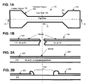
- FIG. 1A is a top view that shows the geometry of a conventional polysilicon fuse 100.
- FIG. 1B is a cross-sectional view taken along line A-A of FIG. 1A.
- polysilicon fuse 100 generally includes two contact regions 102, 108 bridged by two transition regions 104, 106 and fuse neck 105. The center of fuse 100 is indicated by the dashed line C.
- Polysilicon fuse 100 is made up of a heavily doped N type (N+) or heavily doped P type (P+) polysilicon layer 110 with or without silicide layer 120 as shown in FIG. 1B.
- the unblown fuse resistance of fuse 100 is preferably low in the range of 50 to 100 ohms (Q).
- Polysilicon fuse 100 becomes electrically open by applying a sufficient amount of energy in a form of current flow so as to blow the fuse.
- both silicide layer 120 and polysilicon layer 110 can be blown open as shown in FIG. 1B.
- the difference in the pre(unblown) and post(blown) fuse resistance values can be made many orders of magnitude such that the blown fuse acts as an open circuit.
- This open state is shown in FIG. 1B by the presence of a gap within fuse neck 105. This gap may not necessarily occur at the center, however, and may instead start at the contact regions.
- CMOS device sizes decrease, it is increasingly difficult to blow a polysilicon fuse since the corresponding supply voltage also becomes small.
- An external power supply is often needed to generate sufficient current flow to create an adequate open fuse state. This is a more costly solution. It is therefore sufficient to blow open only the silicide layer to program the polysilicon fuse. This can be done by the limited internal power supply.
- FIGs. 2A and 2B show one conventional polysilicon fuse 200 used as a programmable element as described in the above-referenced Alvai article.
- polysilicon fuse 200 is formed from a silicide layer 220 on the top of a polysilicon layer 210.
- Polysilicon layer 210 can be undoped, N+ doped, or P+ doped as shown in Fig. 2A.
- Silicide layer 220 can include titanium silicide, nickel silicide, platinum silicide, or cobalt silicide.
- FIG. 2B shows fuse 200 in an open state where the silicide layer has been programmed to create a region 230 where the resistance is made higher because current is now conducted through the higher resistance polysilicon layer 210. The break in the silicide layer may not necessarily occur at the center, however, and may instead start at the contact regions.
- Region 230 is created by passing electrical current through silicide layer 220 as part of an agglomeration process.
- the location where region 230 occurs along fuse 200 is referred to the "fusing location.”
- the fusing location has been reported to be a function of temperature gradient in addition to fuse geometry and pre fuse resistance. See , Alvai, M., et al ., IEDM :855-858 (1997).
- the present invention provides an integrated fuse with regions of different doping located within a fuse neck. During a fusing event, a distribution of temperature peaks occur around the regions of different dopants. By locating regions of different dopants within the fuse neck, agglomeration starts reliably and efficiently within the fuse neck (for example, at or near the center of the fuse neck) and proceeds toward the contact regions.
- integrated fuses according to the present invention can include an improved post fuse resistance distribution and an increased minimum resistance value in the post fuse resistance distribution compared to conventional polysilicon fuses.
- Integrated fuses of the present invention can be used in variety of applications including but not limited to programmable elements.
- an integrated fuse has a polysilicon layer and a silicide layer.
- the polysilicon layer includes first and second regions each having an end within the fuse neck of the integrated fuse.
- the first and second regions have first and second types of dopants. These types of dopants are different.
- the first type of dopant in the first region comprises an N-type dopant and the second type of dopant in the second region comprises a P-type dopant.
- the first region and second regions are adjacent to one another such that each of the one ends of the first and second regions meet or abut at a common interface.
- the common interface is located at or near the center of the fuse neck region.
- the first type of dopant in the first region is a heavily-doped N-type dopant and the second type of dopant in the second region is a heavily-doped P-type dopant.
- the first type of dopant in the first region is a lightly-doped N-type dopant and the second type of dopant in the second region is a lightly-doped P-type dopant.
- the polysilicon layer further includes a third region located at or near the center of the fuse neck region and in between first and second regions of the polysilicon layer.
- the third region is undoped, while the first type of dopant in the first region is a heavily-doped N-type dopant and the second type of dopant in the second region is a heavily-doped P-type dopant.
- the third region is undoped, while the first type of dopant in the first region is a lightly-doped N-type dopant and the second type of dopant in the second region is a lightly-doped P-type dopant.
- the polysilicon layer further includes a third region which is lightly doped with N-type and P-type dopants. First and second regions next to the third region are lightly-doped with respective N-type and P-type dopants.
- the polysilicon layer further includes a third region which is heavily doped with N-type and P-type dopants. First and second regions next to the third region are then heavily-doped with respective N-type and P-type dopants.
- the present invention includes a method for making an integrated fuse.
- the method includes steps of forming a polysilicon layer that includes first and second regions having different first and second types of dopants, and forming a silicide layer along the polysilicon layer.
- the present invention provides an integrated fuse with regions of different doping located within a fuse neck. During a fusing event, a distribution of temperature peaks occur around the regions of different dopants. By locating regions of different dopants within the fuse neck, agglomeration starts reliably and efficiently within the fuse neck (for example, at or near the center of the fuse neck) and proceeds toward the contact regions. Further advantages of integrated fuses according to the present invention can include an improved post fuse resistance distribution and an increased minimum resistance value in the post fuse resistance distribution compared to conventional polysilicon fuses.
- Integrated fuses of the present invention can be used in variety of applications including, but not limited to, fuses, programmable elements, programmable read only memory (PROM), static random access memory (SRAM), redundancy implementation in logic devices, die identification, electrically programmable feature selection, and CMOS logic elements.
- PROM programmable read only memory
- SRAM static random access memory
- FIGs. 3A, 3B, 4A, 4B, 5A, and 5B are cross-sectional views of integrated fuses according to embodiments of the present invention.
- Each of the cross-sectional views in FIGS. 3A-5B is taken along a plane extending through the respective integrated fuses and including a center of a fuse neck region between two contact regions.
- Each of the integrated fuses shown in FIGs. 3A-5B can have any conventional fuse geometry and shape including, but not limited to, the fuse shape shown in FIG. 1.
- FIGs. 3A and 3B show integrated fuses 300A, 300B in a butted configuration according to the present invention.
- integrated fuse 300A includes a polysilicon layer having a first region 310A and a second region 312A.
- Silicide layer 320 is formed on the polysilicon regions 310A, 312A.
- One end of each of the regions 310A, 312A abut each other at a common interface 314A.
- Common interface 314A is located at or near the center of a fuse neck region.
- First region 310A comprises polysilicon with heavily-doped N-type (N+) dopants.
- Second region 312A comprises polysilicon with heavily-doped P-type (P+) dopants.
- first region 310A can comprise polysilicon with P+ dopants
- second region 312A can comprise polysilicon with N+ dopants.
- integrated fuse 300B includes silicide layer 320 and a polysilicon layer having a first region 310B and a second region 312B. One end of each of the regions 310B, 312B abut each other at a common interface 314B. Common interface 314B is located at or near the center of a fuse neck region.
- First region 310B comprises polysilicon with lightly-doped N-type (NLdd) dopants.
- Second region 312B comprises polysilicon with lightly-doped P-type (PLdd) dopants. In this way, a fusing event is initiated within the fuse neck region at center C when the integrated fuse receives an electrical current stress.
- first region 310B can comprise polysilicon with PLdd dopants
- second region 312B can comprise polysilicon with NLdd dopants.
- FIGs. 4A and 4B show integrated fuses 400A, 400B in a spaced configuration with an undoped center according to the present invention.
- integrated fuse 400A includes a polysilicon layer having a first region 410A and a second region 412A separated by an undoped region 414A.
- Silicide layer 320 is formed on the polysilcon regions 410A, 412A, and 414A.
- Undoped region 414A is located between regions 410A, 412A at or near the center C in the fuse neck region of integrated fuse 400A.
- First region 410A comprises polysilicon with heavily-doped N-type (N+) dopants.
- Second region 412A comprises polysilicon with heavily-doped P-type (P+) dopants.
- Undoped region 414A is made of undoped polysilicon. In this way, a fusing event is initiated within the fuse neck region at the undoped region 414A at or near center C when the integrated fuse receives an electrical current stress.
- first region 410A can comprise polysilicon with P+ dopants
- second region 412A can comprise polysilicon with N+ dopants.
- integrated fuse 400B includes a polysilicon layer having a first region 410B and a second region 412B separated by an undoped region 414B.
- Silicide layer 320 is formed on the polysilcon regions 410B, 412B, and 414B.
- Undoped region 414B is located between regions 410B, 412B at or near the center C in the fuse neck region of integrated fuse 400B.
- First region 410B comprises polysilicon with lightly-doped N-type (NLdd) dopants.
- Second region 412B comprises polysilicon with lightly-doped P-type (PLdd) dopants.
- Undoped region 414B is made of undoped polysilicon.
- first region 410B can comprise polysilicon with PLdd dopants
- second region 412B can comprise polysilicon with NLdd dopants.
- FIGs. 5A and 5B show integrated fuses 500A, 500B in a spaced configuration with a doped center according to the present invention.
- integrated fuse 500A includes a polysilicon layer having a first region 510A and a second region 512A separated by a doped region 514A.
- Silicide layer 320 is formed on polysilicon regions 510A, 512A, and 514A.
- Doped region 514A is located between regions 510A, 512A at or near the center C in the fuse neck region of integrated fuse 500A.
- First region 510A comprises polysilicon with lightly-doped N-type (NLdd) dopants.
- Second region 512A comprises polysilicon with lightly-doped P-type (PLdd) dopants.
- Doped region 514A is made up of polysilicon with lightly doped P-type and lightly-doped N-type dopants. In this way, a fusing event is initiated within the fuse neck region at the undoped region 514A at or near center C when the integrated fuse receives an electrical current stress.
- first region 510A can comprise polysilicon with PLdd dopants
- second region 512A can comprise polysilicon with NLdd dopants.
- integrated fuse 500B includes a polysilicon layer having a first region 510B and a second region 512B separated by a doped region 514B.
- Silicide layer 320 is formed on polysilicon regions 510B, 512B, and 514B.
- Doped region 514B is located between regions 510B, 512B at or near the center C in the fuse neck region of integrated fuse 500B.
- First region 510B comprises polysilicon with heavily-doped N-type (N+) dopants.
- Second region 512B is comprises polysilicon with heavily-doped P-type (P+) dopants.
- Doped region 514B is made up of polysilicon with heavily-doped P-type (P+) and heavily-doped N-type (N+) dopants. In this way, a fusing event is initiated within the fuse neck region at the undoped region 514B at or near center C when the integrated fuse receives an electrical current stress.
- first region 510B can comprise polysilicon with P+ dopants
- second region 512B can comprise polysilicon with N+ dopants.
- silicide layer 320 can include, but is not limited to, any one of the following materials: titanium silicide, nickel silicide, platinum silicide, or cobalt silicide.
- the polysilicon layer including regions 310A, 312A, 310B, 312B, 410A, 412A, 414A, 410B, 412B, 414B, 510A, 512A, 514A, 510B, 512B, and 514B can be formed on an isolation field oxide, such as, SiO 2 .
- the present invention can be used with lightly and/or heavily doped N and P dopants as described above. Any conventional doping ranges for lightly and/or heavily doped N and P dopants in polysilicon can be used as would be apparent to person skilled in the art given this description.
- Example ranges of dopants include the following: a range of 1x10 13 to 5x10 14 ions/cm 2 for lightly doped N dopants; a range of 1x10 13 to 5x10 14 ions/cm 2 for lightly doped P dopants; a range of 1x10 15 to 1x10 16 ions/cm 2 for heavily doped N dopants; and a range of 1x10 15 to 1x10 16 ions/cm 2 for heavily doped P dopants. These example ranges however are illustrative and not intended to limit the present invention.
- polysilicon fuses 300A, 300B, 400A, 400B, 500A, 500B described above can have a tight post fuse resistance distribution and a high value of minimum post fuse resistance compared to conventional polysilicon fuses having a homogenous layer of polysilicon.
- the polysilicon fuses according to the present invention have a structure that ensures agglomeration reliably starts at or very near the center of the fuse neck (where the different doping regions meet) and proceeds toward the beginning of the contact regions.
- polysilicon fuses 300A, 300B, 400A, 400B, 500A, 500B as described above, have regions of different doping within the fuse neck. These regions, which are formed prior to silicidation, create temperature distributions with one or more peaks at or around the center of the fuse neck region. Each peak coincides with a boundary between regions having different dopants (e.g., the N+/P+ butted, NLdd/PLdd butted, undoped, PLdd and NLdd, N+ and P+ regions).
- N+ and P+ dopants in the polysilicon fuse diffuse to the undoped region to form a lightly doped N+/P+ junction for the P+/undoped/N+ polysilicon structure.
- the depletion layer becomes larger due to the dopant diffusion.
- the thermal conductivity is generally proportional to the conductivity of material.
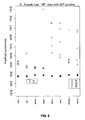
- FIG. 6 shows a plot of pre and post fuse resistance values obtained in tests that compared a conventional polysilicon fuse having a homogenous N+ polysilicon layer with an integrated fuse having a polysilicon layer with a N+/P+ butted region according to the invention.
- Five dies (dies 1-5) of samples were tested.
- Test data for samples of the conventional polysilicon fuse having a homogenous N+ polysilicon layer (N41V, N41, N41AV, N41A) is plotted along the bottom axis.
- Test data for samples of the fuse having a polysilicon layer with N+/P+ butted regions according to the invention (NP41V, NP41, NP41AV, NP41A) is also plotted along the bottom axis.
- Pre and post fuse resistance values in ohms for these fuse samples are plotted along the side axis.
- the combination of a P/N junction and greater temperature gradient in fuse structures with N+/P+ butted regions according to the invention maximizes the post fuse resistance and increases the minimum value of the distribution of the post fuse resistance.
- FIG. 7 is a plot of the cumulative probability of post fuse resistance values generated from the same samples shown in FIG. 6.
- the plot clearly shows that the post fuse resistance is higher for a fuse having a polysilicon layer with N+/P+ butted regions according to the invention compared to a conventional polysilicon fuse having a homogenous N+ polysilicon layer.
- the plot also shows that there is an increase in the minimum value of post fuse resistance for a fuse having a polysilicon layer with N+/P+ butted regions according to the invention, compared to a conventional polysilicon fuse having a homogenous N+ polysilicon layer.
- FIG. 8 shows a method 800 for making an integrated fuse according to an embodiment of the present invention (steps 810-820).
- a polysilicon layer is formed that includes regions having different types of dopants (step 810).
- a silicide layer is formed on the polysilicon layer (step 820).
- steps can be carried out using any conventional semiconductor manufacturing process, including but not limited to a CMOS process, as would be apparent to a person skilled in the art given this description. For instance, an undoped polysilicon layer is deposited and etched to form the polysilicon fuse layer, after one or more gate oxide layers are grown for a standard CMOS logic process.
- the N+, P+, NLdd, and PLdd regions (310A, 312A, 310B, 312B, 410A, 412A, 410B, 412B, 510A, 512A, 510B, 512B) in FIGs. 3A, 3B, 4A, 4B, 5A and 5B can be defined and formed by NLDD and PLDD masks and ion implantations of P and N dopants with a dose of 1x10 13 - 5x10 14 ions / cm 2 before a spacer oxide is formed.
- the cross hatched area 514A in FIG. 5A receives both NLdd and PLdd dopants.
- silicide layer 320 can be formed by a deposition, for example, of one of the materials, cobalt, nickel, titanium, platinum and/or other silicide material, and proper heat treatments. Then the integrated fuse is defined by etching the non-silicide material away.
Landscapes
- Design And Manufacture Of Integrated Circuits (AREA)
Abstract
Description
Claims (19)
- An integrated fuse having a fuse neck region in between two contact regions, comprising:wherein said first and second regions of said polysilicon layer each have one end located in the fuse neck region, and said first and second types of dopants are different types of dopants, whereby, a fusing event is initiated within the fuse neck region when the integrated fuse receives an electrical current stress.a polysilicon layer that includes first and second regions having first and second types of dopants, respectively; anda silicide layer formed on the polysilicon layer;
- The integrated fuse of claim 1, wherein said first region and said second region are adjacent to one another such that each of the one ends of the first and second regions meet at a common interface, said common interface being located at or near the center of the fuse neck region.
- The integrated fuse of claim 1, wherein said first type of dopant in said first region comprises an N-type dopant and said second type of dopant in said second region comprises a P-type dopant.
- The integrated fuse of claim 1, wherein said first type of dopant in said first region comprises a heavily-doped N-type dopant and said second type of dopant in said second region comprises a heavily-doped P-type dopant.
- The integrated fuse of claim 1, wherein said first type of dopant in said first region comprises a lightly-doped N-type dopant and said second type of dopant in said second region comprises a lightly-doped P-type dopant.
- The integrated fuse of claim 1, wherein said polysilicon layer further includes a third region located at or near the center of the fuse neck region . and in between said first and second regions.
- The integrated fuse of claim 1, wherein said third region comprises a region of undoped polysilicon.
- The integrated fuse of claim 7, wherein said first type of dopant in said first region comprises an N-type dopant and said second type of dopant in said second region comprises a P-type dopant.
- The integrated fuse of claim 7, wherein said first type of dopant in said first region comprises a heavily-doped N-type dopant and said second type of dopant in said second region comprises a heavily-doped P-type dopant.
- The integrated fuse of claim 7, wherein said first type of dopant in said first region comprises a lightly-doped N-type dopant and said second type of dopant in said second region comprises a lightly-doped P-type dopant.
- The integrated fuse of claim 6, wherein said third region comprises a region of lightly-doped P-type and lightly-doped N-type polysilicon.
- The integrated fuse of claim 11, wherein said first type of dopant in said first region comprises a lightly-doped N-type dopant and said second type of dopant in said second region comprises a lightly-doped P-type dopant.
- The integrated fuse of claim 6, wherein said third region comprises a region of heavily-doped P-type and heavily-doped N-type polysilicon.
- The integrated fuse of claim 13, wherein said first type of dopant in said first region comprises a heavily-doped N-type dopant and said second type of dopant in said second region comprises a heavily-doped P-type dopant.
- The integrated fuse of claim 1, wherein said silicide layer includes at least one of the following materials: titanium silicide, nickel silicide, platinum silicide, or cobalt silicide.
- A programmable element comprising:wherein said first and second regions of said polysilicon layer each have one end located in the fuse neck region, and said first and second types of dopants are different types of dopants, whereby, a programmable fusing event is initiated within the fuse neck region when the integrated fuse receives an electrical current stress.an integrated fuse having a fuse neck region in between two contact regions, the integrated fuse including:a polysilicon layer with first and second regions having first and second types of dopants, respectively; anda silicide layer formed on the polysilicon layer;
- A method for making an integrated fuse having a fuse neck region in between two contact regions, comprising:forming a polysilicon layer that includes first and second regions having first and second types of dopants, respectively; andforming a silicide layer on the polysilicon layer; wherein said first and second regions of said polysilicon layer each have one end located in the fuse neck region, and said first and second types of dopants are different types of dopants, whereby, a fusing event is initiated within the fuse neck region when the integrated fuse receives an electrical current stress.
- An integrated fuse having a fuse neck region in between two contact regions, comprising:a first layer that includes first and second regions having first and second types of dopants, respectively; wherein said first and second regions of said first layer each have one end located in the fuse neck region, and said first and second types of dopants are different types of dopants, whereby, a fusing event is initiated within the fuse neck region when the integrated fuse receives an electrical current stress.
- The integrated fuse of claim 18, wherein said first layer comprises polysilicon.
Applications Claiming Priority (2)
| Application Number | Priority Date | Filing Date | Title |
|---|---|---|---|
| US10/115,013 US6580156B1 (en) | 2002-04-04 | 2002-04-04 | Integrated fuse with regions of different doping within the fuse neck |
| US115013 | 2005-04-26 |
Publications (3)
| Publication Number | Publication Date |
|---|---|
| EP1351254A2 true EP1351254A2 (en) | 2003-10-08 |
| EP1351254A3 EP1351254A3 (en) | 2006-09-20 |
| EP1351254B1 EP1351254B1 (en) | 2010-12-15 |
Family
ID=22358812
Family Applications (1)
| Application Number | Title | Priority Date | Filing Date |
|---|---|---|---|
| EP03007698A Expired - Lifetime EP1351254B1 (en) | 2002-04-04 | 2003-04-03 | An integrated fuse with regions of different doping within the fuse neck |
Country Status (3)
| Country | Link |
|---|---|
| US (3) | US6580156B1 (en) |
| EP (1) | EP1351254B1 (en) |
| DE (1) | DE60335320D1 (en) |
Cited By (1)
| Publication number | Priority date | Publication date | Assignee | Title |
|---|---|---|---|---|
| US8809997B2 (en) | 2011-06-17 | 2014-08-19 | Samsung Electronics Co., Ltd. | E-fuse structures and methods of operating and manufacturing the same |
Families Citing this family (42)
| Publication number | Priority date | Publication date | Assignee | Title |
|---|---|---|---|---|
| US6580156B1 (en) * | 2002-04-04 | 2003-06-17 | Broadcom Corporation | Integrated fuse with regions of different doping within the fuse neck |
| USRE50035E1 (en) * | 2003-03-31 | 2024-07-09 | Sony Group Corporation | Semiconductor device |
| US20050127475A1 (en) * | 2003-12-03 | 2005-06-16 | International Business Machines Corporation | Apparatus and method for electronic fuse with improved esd tolerance |
| US7106164B2 (en) * | 2003-12-03 | 2006-09-12 | International Business Machines Corporation | Apparatus and method for electronic fuse with improved ESD tolerance |
| US6956277B1 (en) * | 2004-03-23 | 2005-10-18 | Taiwan Semiconductor Manufacturing Company, Ltd. | Diode junction poly fuse |
| CN100346449C (en) * | 2004-05-19 | 2007-10-31 | 上海宏力半导体制造有限公司 | Method for forming polycrystalline silicon thin film with high value of resistance |
| US20050258505A1 (en) * | 2004-05-20 | 2005-11-24 | Taiwan Semiconductor Manufacturing Co., Ltd. | Mixed implantation on polysilicon fuse for CMOS technology |
| US7304366B2 (en) * | 2004-08-02 | 2007-12-04 | Taiwan Semiconductor Manufacturing Co., Ltd. | Self correcting multiple-link fuse |
| US20060071298A1 (en) * | 2004-10-05 | 2006-04-06 | Hui Kelvin Y | Polysilicon memory element |
| US7284168B2 (en) * | 2005-01-26 | 2007-10-16 | Hewlett-Packard Development Company, L.P. | Method and system for testing RAM redundant integrated circuits |
| US7321501B2 (en) * | 2005-06-09 | 2008-01-22 | United Microelectronics Corp. | Method for trimming programmable resistor to predetermined resistance |
| US7659168B2 (en) * | 2005-11-03 | 2010-02-09 | International Business Machines Corporation | eFuse and methods of manufacturing the same |
| US20070222027A1 (en) * | 2006-03-27 | 2007-09-27 | Yang Jeong-Hwan | Electronic fuse elements with constricted neck regions that support reliable fuse blowing |
| US7576407B2 (en) | 2006-04-26 | 2009-08-18 | Samsung Electronics Co., Ltd. | Devices and methods for constructing electrically programmable integrated fuses for low power applications |
| US20070262413A1 (en) * | 2006-05-11 | 2007-11-15 | Booth Roger A Jr | E-fuse and method for fabricating e-fuses integrating polysilicon resistor masks |
| US7855414B2 (en) | 2006-07-28 | 2010-12-21 | Broadcom Corporation | Semiconductor device with increased breakdown voltage |
| US20080246080A1 (en) * | 2006-07-28 | 2008-10-09 | Broadcom Corporation | Shallow trench isolation (STI) based laterally diffused metal oxide semiconductor (LDMOS) |
| US7710236B2 (en) * | 2006-08-01 | 2010-05-04 | Delphi Technologies, Inc. | Fuse systems with serviceable connections |
| US20080036033A1 (en) * | 2006-08-10 | 2008-02-14 | Broadcom Corporation | One-time programmable memory |
| KR20080054791A (en) * | 2006-12-13 | 2008-06-19 | 삼성전자주식회사 | Fuse structure of semiconductor device |
| US7732898B2 (en) * | 2007-02-02 | 2010-06-08 | Infineon Technologies Ag | Electrical fuse and associated methods |
| US7851885B2 (en) * | 2007-03-07 | 2010-12-14 | International Business Machines Corporation | Methods and systems involving electrically programmable fuses |
| US7732893B2 (en) * | 2007-03-07 | 2010-06-08 | International Business Machines Corporation | Electrical fuse structure for higher post-programming resistance |
| US8076754B2 (en) * | 2007-03-09 | 2011-12-13 | Silicon Laboratories | Silicide-interface polysilicon resistor |
| US7619295B2 (en) * | 2007-10-10 | 2009-11-17 | Fairchild Semiconductor Corporation | Pinched poly fuse |
| KR20090070826A (en) * | 2007-12-27 | 2009-07-01 | 주식회사 하이닉스반도체 | Semiconductor device with fuse and method for manufacturing same |
| KR100979367B1 (en) * | 2008-03-19 | 2010-08-31 | 주식회사 하이닉스반도체 | Fuse formation method of semiconductor device |
| US8013419B2 (en) * | 2008-06-10 | 2011-09-06 | International Business Machines Corporation | Structure and method to form dual silicide e-fuse |
| US8003474B2 (en) * | 2008-08-15 | 2011-08-23 | International Business Machines Corporation | Electrically programmable fuse and fabrication method |
| TWI397987B (en) * | 2009-02-24 | 2013-06-01 | 晨星半導體股份有限公司 | Electronic fuse and its related control circuit |
| JP5499493B2 (en) * | 2009-03-05 | 2014-05-21 | 東芝ライテック株式会社 | lighting equipment |
| US8072049B2 (en) * | 2009-04-24 | 2011-12-06 | Fairchild Semiconductor Corporation | Polysilicon drift fuse |
| US20100295126A1 (en) * | 2009-05-22 | 2010-11-25 | Broadcom Corporation | High dielectric constant gate oxides for a laterally diffused metal oxide semiconductor (LDMOS) |
| US8203188B2 (en) * | 2009-05-22 | 2012-06-19 | Broadcom Corporation | Split gate oxides for a laterally diffused metal oxide semiconductor (LDMOS) |
| US8274114B2 (en) | 2010-01-14 | 2012-09-25 | Broadcom Corporation | Semiconductor device having a modified shallow trench isolation (STI) region and a modified well region |
| US8283722B2 (en) | 2010-06-14 | 2012-10-09 | Broadcom Corporation | Semiconductor device having an enhanced well region |
| US9123807B2 (en) | 2010-12-28 | 2015-09-01 | Broadcom Corporation | Reduction of parasitic capacitance in a semiconductor device |
| CN103872011B (en) * | 2012-12-18 | 2016-08-31 | 中芯国际集成电路制造(上海)有限公司 | Electrically programmable fuse structure |
| CN104425446B (en) * | 2013-08-20 | 2017-12-29 | 中芯国际集成电路制造(上海)有限公司 | Electric fuse structure and its application method |
| FR3063573B1 (en) * | 2017-03-01 | 2019-05-03 | Stmicroelectronics (Rousset) Sas | INTEGRATED FUSE DEVICE |
| JP2018170455A (en) * | 2017-03-30 | 2018-11-01 | エイブリック株式会社 | Semiconductor device |
| CN115707237B (en) * | 2021-08-09 | 2025-11-14 | 无锡华润上华科技有限公司 | A polysilicon fuse-type non-volatile memory and its fabrication method |
Family Cites Families (8)
| Publication number | Priority date | Publication date | Assignee | Title |
|---|---|---|---|---|
| US6337507B1 (en) * | 1995-09-29 | 2002-01-08 | Intel Corporation | Silicide agglomeration fuse device with notches to enhance programmability |
| US5708291A (en) * | 1995-09-29 | 1998-01-13 | Intel Corporation | Silicide agglomeration fuse device |
| US5976943A (en) * | 1996-12-27 | 1999-11-02 | Vlsi Technology, Inc. | Method for bi-layer programmable resistor |
| US6088256A (en) * | 1998-09-25 | 2000-07-11 | Stmicroelectronics, Inc. | Integrated circuit with electrically programmable fuse resistor |
| US6570227B2 (en) * | 1999-06-23 | 2003-05-27 | Bae Systems Information And Electronics Systems Integration, Inc. | High-performance high-density CMOS SRAM cell |
| US6525397B1 (en) * | 1999-08-17 | 2003-02-25 | National Semiconductor Corporation | Extended drain MOSFET for programming an integrated fuse element to high resistance in low voltage process technology |
| US6323535B1 (en) * | 2000-06-16 | 2001-11-27 | Infineon Technologies North America Corp. | Electrical fuses employing reverse biasing to enhance programming |
| US6580156B1 (en) * | 2002-04-04 | 2003-06-17 | Broadcom Corporation | Integrated fuse with regions of different doping within the fuse neck |
-
2002
- 2002-04-04 US US10/115,013 patent/US6580156B1/en not_active Expired - Fee Related
-
2003
- 2003-04-03 EP EP03007698A patent/EP1351254B1/en not_active Expired - Lifetime
- 2003-04-03 DE DE60335320T patent/DE60335320D1/en not_active Expired - Lifetime
- 2003-04-09 US US10/409,584 patent/US6770948B2/en not_active Expired - Fee Related
-
2004
- 2004-06-21 US US10/871,569 patent/US7227238B2/en not_active Expired - Fee Related
Cited By (1)
| Publication number | Priority date | Publication date | Assignee | Title |
|---|---|---|---|---|
| US8809997B2 (en) | 2011-06-17 | 2014-08-19 | Samsung Electronics Co., Ltd. | E-fuse structures and methods of operating and manufacturing the same |
Also Published As
| Publication number | Publication date |
|---|---|
| US20040222491A1 (en) | 2004-11-11 |
| US20030205777A1 (en) | 2003-11-06 |
| US6580156B1 (en) | 2003-06-17 |
| US7227238B2 (en) | 2007-06-05 |
| EP1351254A3 (en) | 2006-09-20 |
| DE60335320D1 (en) | 2011-01-27 |
| US6770948B2 (en) | 2004-08-03 |
| EP1351254B1 (en) | 2010-12-15 |
Similar Documents
| Publication | Publication Date | Title |
|---|---|---|
| EP1351254B1 (en) | An integrated fuse with regions of different doping within the fuse neck | |
| US6956277B1 (en) | Diode junction poly fuse | |
| KR101006123B1 (en) | Electrically programmable fuses for insulator-phase-silicon (SOI) technology | |
| US6979601B2 (en) | Methods for fabricating fuses for use in semiconductor devices and semiconductor devices including such fuses | |
| US8299570B2 (en) | Efuse containing sige stack | |
| US8163640B2 (en) | Metal gate compatible electrical fuse | |
| US7960809B2 (en) | eFuse with partial SiGe layer and design structure therefor | |
| US20060263946A1 (en) | Recessed gate dielectric antifuse | |
| US20090140382A1 (en) | Electric fuse device made of polysilicon silicide | |
| US20080029843A1 (en) | E-Fuse and Method for Fabricating E-Fuses Integrating Polysilicon Resistor Masks | |
| WO1995008845A1 (en) | Field programmable read only memory (rom) cell using an amorphous silicon antifuse with buried contact polysilicon and metal electrodes | |
| JP2009515330A (en) | Electrically programmable fuse and method of manufacturing the same | |
| EP1831927B1 (en) | An anti-fuse cell and its manufacturing process | |
| US20220149051A1 (en) | Non-volatile memory elements with one-time or multiple-time programmability | |
| US7425472B2 (en) | Semiconductor fuses and semiconductor devices containing the same | |
| US9852983B1 (en) | Fabricating method of anti-fuse structure | |
| US20050124097A1 (en) | Integrated circuit with two phase fuse material and method of using and making same | |
| CN118571860B (en) | Fuse device and forming method | |
| US20100187638A1 (en) | Anti-fuse cell and its manufacturing process |
Legal Events
| Date | Code | Title | Description |
|---|---|---|---|
| PUAI | Public reference made under article 153(3) epc to a published international application that has entered the european phase |
Free format text: ORIGINAL CODE: 0009012 |
|
| AK | Designated contracting states |
Kind code of ref document: A2 Designated state(s): AT BE BG CH CY CZ DE DK EE ES FI FR GB GR HU IE IT LI LU MC NL PT RO SE SI SK TR |
|
| AX | Request for extension of the european patent |
Extension state: AL LT LV MK |
|
| PUAL | Search report despatched |
Free format text: ORIGINAL CODE: 0009013 |
|
| AK | Designated contracting states |
Kind code of ref document: A3 Designated state(s): AT BE BG CH CY CZ DE DK EE ES FI FR GB GR HU IE IT LI LU MC NL PT RO SE SI SK TR |
|
| AX | Request for extension of the european patent |
Extension state: AL LT LV MK |
|
| 17P | Request for examination filed |
Effective date: 20070320 |
|
| AKX | Designation fees paid |
Designated state(s): DE FR GB |
|
| RAP1 | Party data changed (applicant data changed or rights of an application transferred) |
Owner name: BROADCOM CORPORATION |
|
| 17Q | First examination report despatched |
Effective date: 20071113 |
|
| GRAP | Despatch of communication of intention to grant a patent |
Free format text: ORIGINAL CODE: EPIDOSNIGR1 |
|
| GRAS | Grant fee paid |
Free format text: ORIGINAL CODE: EPIDOSNIGR3 |
|
| GRAA | (expected) grant |
Free format text: ORIGINAL CODE: 0009210 |
|
| AK | Designated contracting states |
Kind code of ref document: B1 Designated state(s): DE FR GB |
|
| REG | Reference to a national code |
Ref country code: GB Ref legal event code: FG4D |
|
| REF | Corresponds to: |
Ref document number: 60335320 Country of ref document: DE Date of ref document: 20110127 Kind code of ref document: P |
|
| PLBE | No opposition filed within time limit |
Free format text: ORIGINAL CODE: 0009261 |
|
| STAA | Information on the status of an ep patent application or granted ep patent |
Free format text: STATUS: NO OPPOSITION FILED WITHIN TIME LIMIT |
|
| 26N | No opposition filed |
Effective date: 20110916 |
|
| REG | Reference to a national code |
Ref country code: DE Ref legal event code: R097 Ref document number: 60335320 Country of ref document: DE Effective date: 20110916 |
|
| REG | Reference to a national code |
Ref country code: FR Ref legal event code: ST Effective date: 20111230 |
|
| PG25 | Lapsed in a contracting state [announced via postgrant information from national office to epo] |
Ref country code: FR Free format text: LAPSE BECAUSE OF NON-PAYMENT OF DUE FEES Effective date: 20110502 |
|
| PGFP | Annual fee paid to national office [announced via postgrant information from national office to epo] |
Ref country code: GB Payment date: 20130422 Year of fee payment: 11 |
|
| PGFP | Annual fee paid to national office [announced via postgrant information from national office to epo] |
Ref country code: DE Payment date: 20140430 Year of fee payment: 12 |
|
| REG | Reference to a national code |
Ref country code: DE Ref legal event code: R119 Ref document number: 60335320 Country of ref document: DE |
|
| GBPC | Gb: european patent ceased through non-payment of renewal fee |
Effective date: 20140403 |
|
| REG | Reference to a national code |
Ref country code: DE Ref legal event code: R119 Ref document number: 60335320 Country of ref document: DE Effective date: 20141101 |
|
| PG25 | Lapsed in a contracting state [announced via postgrant information from national office to epo] |
Ref country code: DE Free format text: LAPSE BECAUSE OF NON-PAYMENT OF DUE FEES Effective date: 20141101 Ref country code: GB Free format text: LAPSE BECAUSE OF NON-PAYMENT OF DUE FEES Effective date: 20140403 |