EP1349434A2 - Lighting circuit, especially for cars - Google Patents
Lighting circuit, especially for cars Download PDFInfo
- Publication number
- EP1349434A2 EP1349434A2 EP03100572A EP03100572A EP1349434A2 EP 1349434 A2 EP1349434 A2 EP 1349434A2 EP 03100572 A EP03100572 A EP 03100572A EP 03100572 A EP03100572 A EP 03100572A EP 1349434 A2 EP1349434 A2 EP 1349434A2
- Authority
- EP
- European Patent Office
- Prior art keywords
- led
- series
- lighting circuit
- row
- strands
- Prior art date
- Legal status (The legal status is an assumption and is not a legal conclusion. Google has not performed a legal analysis and makes no representation as to the accuracy of the status listed.)
- Granted
Links
Images


Classifications
-
- H—ELECTRICITY
- H05—ELECTRIC TECHNIQUES NOT OTHERWISE PROVIDED FOR
- H05B—ELECTRIC HEATING; ELECTRIC LIGHT SOURCES NOT OTHERWISE PROVIDED FOR; CIRCUIT ARRANGEMENTS FOR ELECTRIC LIGHT SOURCES, IN GENERAL
- H05B45/00—Circuit arrangements for operating light-emitting diodes [LED]
- H05B45/40—Details of LED load circuits
Definitions
- the invention relates to a lighting circuit, in particular for motor vehicles.
- Such lighting circuits are increasingly being built up with light-emitting diodes as illuminants.
- illuminants light-emitting diodes
- a different number of LEDs is required. This raises the question of the circuit arrangement in which the LEDs are arranged.
- a series connection of all LEDs would have the disadvantage that if one LED fails, all LEDs would fail.
- a compromise between these two extremes is a combined series / parallel connection in which the series connected in parallel are networked with one another to form a light-emitting diode matrix.
- Such a light-emitting diode matrix consists of n rows connected in parallel, each with m strings connected in series, a light-emitting diode being arranged in each strand and an electrically conductive cross-connection running between the strings of each row to the adjacent rows.
- the cross connections ensure that if one LED fails, the other LEDs continue to be supplied with power and can continue to light up.
- Such a light-emitting diode matrix for motor vehicles is known, for example, from EP 0896 899A2.
- the cross connections between the rows are realized by cables or conductor tracks, whose ohmic resistance is negligibly small.
- LEDs be uniformly bright glow so that a homogeneous lighting impression is created.
- a light-emitting diode matrix is preferably only fitted with LEDs which are in the same Voltage class are, the voltage class being within the range of values of the permissible Relates to foot tensions.
- the LEDs of a voltage class also differ with regard to their diode characteristic within a tolerance range. This leads to the fact that unfavorable constellations the currents through the different strands of the LED matrix can be very different; in extreme cases they can look around distinguish the factor 2 and more. This in turn has an undesirable effect different brightnesses. In addition, this can lead to the rated currents certain LEDs in the light-emitting diode matrix are clearly exceeded, which is negative affects the life of the LEDs.
- each LED is proposed in EP 0 793 402 B1 assign a resistor to a string in series. This will create a similar linearization of different LED characteristics achieved and thus overall an even current distribution across the different strings / LEDs.
- the large number of resistors that is needed, however, is problematic because it involves high component and Assembly costs are connected. It is also for the multitude of resistors additional installation space required.
- Another problem is that over the in series switched resistors each drop a voltage that is a thermal power loss generated. The thermal power loss reduces the efficiency of the Light generation and on the other hand cause by the thermal power loss generated high temperatures an increased degradation of the LEDs.
- the object of the invention is to provide a lighting circuit for an LED matrix create, which overcomes the disadvantages listed above.
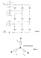
- FIG. 1 shows an LED matrix according to the prior art according to EP 0896 899A2 shown. It consists of a combined series / parallel connection with two rows each have 3 strands. There is an LED in each strand. Between Strands of each row an electrically conductive connection is arranged, the ohmic resistance is practically zero.
- the LED matrix is over a series resistor (Rv) connected to the supply voltage.
- a protective diode serves as reverse polarity protection.
- FIG. 2 shows an LED matrix according to the prior art according to EP 0793 402 B1 shown. A series resistor of an LED is connected in series in each line.
- FIG. 3 shows a lighting circuit with a 6-LED matrix, as in FIG. 1, however is a transverse resistance according to the invention in the cross connections between the strands built-in.
- the effect achieved according to the invention, which is achieved with the transverse resistances is explained with reference to Figures 7 and 8.
- the characteristic curves for the LED are shown in FIG with the number 4 and the LED with the number 3.
- the LED with the number 4 should Have a forward voltage at the bottom of the tolerance range of a voltage class lies, while the forward voltage of the LED with the number 3 is at the upper edge.
- the forward voltages of the other LEDs (1, 2, 5, 6) are the same and are in the middle of the Tolerance band.
- the nominal current of the LEDs is 50 m ampere.
- This current difference causes a different brightness of the LEDs and causes permanent degradation of the LEDs.
- With increasing transverse resistance the current difference then decreases, the currents approaching the nominal current. From The currents then approximated the nominal current at a maximum of approx. 80 ⁇ .
- the LED matrix is over series resistors connected to the supply voltage (Vcc). It can be the number of in a row LEDs connected in series are selected according to the forward voltage (approx. 2 to 3V) be that the voltage drop across all LEDs connected in series (Functional voltage limit) as close as possible to the lower limit of the Supply voltage is approaching. In a motor vehicle, the supply voltage decrease from 14 volts to 9 volts in the short term.
- the serves Series resistor to adjust the current that flows into the LED matrix. To the To distribute power loss evenly, preferably two or more in parallel switched series resistors (Rv) provided.
- the LED matrix In contrast to the lighting circuit according to EP 0 793 402 B1, where the Series resistors are also arranged in the LED matrix in series with the LEDs, can the LED matrix with the thermal in the lighting circuit according to the invention lightly loaded transverse resistances in the housing of a luminous element (e.g. headlights or rear light), while the series resistor or resistors outside the Housing can be arranged. This eliminates the annoying heat loss from the inside kept away from the housing.
- these are Series resistors included in the housing as part of the LED matrix.
- the equalizing currents independent of the load current through the LEDs.
- the LED matrix is a Constant current source, which is a constant regardless of voltage fluctuations Provides electricity.
- a low, optimal to the Functional voltage limit adapted supply voltage can be selected because the Voltage drop across the series resistors in the strands according to EP 0 793 402 B1 is eliminated.
- Figure 4 is the embodiment of a lighting circuit with a 9 LED matrix consisting of 3 rows connected in parallel, each with three strands. It is between the first and the second strand of the first row and between the first and a transverse resistor is arranged in the second strand of the second row. Likewise, between the first and the second strand of the second row and between the first and the a second resistor in the third row of the third row is arranged. Appropriate Cross resistances are also found between the second and third strands of each neighboring rows.
- the lighting circuit according to Figure 4 is analogous to Illumination circuit according to FIG. 3. In contrast to FIG.
- the shunt resistors are connected at one end to a common star account point and at the other end to a row in the area between two strands.
- this star connection is shown again for clarification alone. The use of such a star connection allows greater design freedom in the layout of the circuit board on which the LED matrix is arranged.
Abstract
Description
Die Erfindung bezieht sich auf einen Beleuchtungsschaltkreis, insbesondere für Kraftfahrzeuge. Solche Beleuchtungsschaltkreise werden zunehmend mit Leuchtdioden als Leuchtmitteln aufgebaut. Je nach Anwendung ist dabei eine unterschiedliche Anzahl von LEDs erforderlich. Dabei stellt sich die Frage nach der Schaltungsanordnung, in der die LEDs angeordnet werden. Eine Reihenschaltung aller LEDs hätte den Nachteil, daß beim Ausfall einer LED sämtliche LEDs ausfallen würden. Eine reine Parallelschaltung aller LEDs hätte, insbesondere bei Kraftfahrzeugen, den Nachteil einer hohen Verlustleistung, da die Bordnetzspannung, die typischerweise 12Volt beträgt, wesentlich höher ist als die Flußspannung einer LED, die typischerweise zwischen 2V und 3 V beträgt, und daher ein entsprechend hoher Spannungsabfall an einem Vorwiderstand zur Anpassung an die LED-Flußspannung notwendig ist, was wiederum eine hohe Verlustleistung an dem Vorwiderstand hervorruft. Ein Kompromiß zwischen diesen beiden Extremen ist eine kombinierte Reihen/Parallelschaltung, in der die parallelgeschalteten Reihen untereinander unter Ausbildung einer Leuchtdiodenmatrix vernetzt sind. Eine derartige Leuchtdiodenmatrix besteht aus n parallelgeschalteten Reihen mit jeweils m hintereinandergeschalteten Strängen, wobei in jedem Strang eine Leuchtdiode angeordnet ist und zwischen den Strängen jeweils einer Reihe eine elektrisch leitende Querverbindung zu den jeweils benachbarten Reihen verläuft. Durch die Querverbindungen wird sichergestellt, daß bei Ausfall einer LED die übrigen LEDs weiter mit Strom versorgt werden und weiterleuchten können. Eine solche Leuchtdiodenmatrix für Kraftfahrzeuge ist beispielsweise aus der EP 0896 899A2 bekannt. Die Querverbindungen zwischen den Reihen sind durch Kabel oder Leiterbahnen realisiert, deren ohmscher Widerstand vernachlässigbar klein ist.The invention relates to a lighting circuit, in particular for motor vehicles. Such lighting circuits are increasingly being built up with light-emitting diodes as illuminants. Depending on the application, a different number of LEDs is required. This raises the question of the circuit arrangement in which the LEDs are arranged. A series connection of all LEDs would have the disadvantage that if one LED fails, all LEDs would fail. A pure parallel connection of all LEDs, especially in motor vehicles, would have the disadvantage of high power dissipation, since the vehicle electrical system voltage, which is typically 12Volt, is significantly higher than the forward voltage of an LED, which is typically between 2V and 3V, and therefore a correspondingly high voltage drop on a series resistor to adapt to the LED forward voltage is necessary, which in turn causes a high power loss at the series resistor. A compromise between these two extremes is a combined series / parallel connection in which the series connected in parallel are networked with one another to form a light-emitting diode matrix. Such a light-emitting diode matrix consists of n rows connected in parallel, each with m strings connected in series, a light-emitting diode being arranged in each strand and an electrically conductive cross-connection running between the strings of each row to the adjacent rows. The cross connections ensure that if one LED fails, the other LEDs continue to be supplied with power and can continue to light up. Such a light-emitting diode matrix for motor vehicles is known, for example, from EP 0896 899A2. The cross connections between the rows are realized by cables or conductor tracks, whose ohmic resistance is negligibly small.
In den meisten Anwendung besteht die Anforderung, daß die LEDs gleichmäßig hell leuchten, damit ein homogener Beleuchtungseindruck entsteht. Zu diesem Zweck werden in einer solchen Leuchtdiodenmatrix vorzugsweise nur LEDs verbaut, die in derselben Spannungsklasse liegen, wobei die Spannungsklasse sich auf den Wertebereich der zulässigen Fußspannungen bezieht. Allerdings unterscheiden sich auch die LEDs einer Spannungsklasse hinsichtlich ihrer Diodenkennlinie innerhalb eines Toleranzbereiches. Dies führt dazu, daß bei ungünstigen Konstellationen die Ströme durch die verschiedenen Stränge der Leuchtdiodenmatrix sehr unterschiedlich sein können; in Extremfällen können sie sich um den Faktor 2 und mehr unterscheiden. Dies bewirkt nun wiederum in unerwünschter Weise unterschiedliche Helligkeiten. Darüber hinaus kann dies dazu führen, daß die Nennströme bestimmter LEDs in der Leuchtdiodenmatrix deutlich überschritten werden, was sich negativ auf die Lebensdauer der LEDs auswirkt.In most applications there is a requirement that the LEDs be uniformly bright glow so that a homogeneous lighting impression is created. For this purpose, in Such a light-emitting diode matrix is preferably only fitted with LEDs which are in the same Voltage class are, the voltage class being within the range of values of the permissible Relates to foot tensions. However, the LEDs of a voltage class also differ with regard to their diode characteristic within a tolerance range. This leads to the fact that unfavorable constellations the currents through the different strands of the LED matrix can be very different; in extreme cases they can look around distinguish the factor 2 and more. This in turn has an undesirable effect different brightnesses. In addition, this can lead to the rated currents certain LEDs in the light-emitting diode matrix are clearly exceeded, which is negative affects the life of the LEDs.
Um diesen Nachteilen zu begegnen wird in der EP 0 793 402 B1 vorgeschlagen, jeder LED eines Stranges einen Widerstand in Reihenschaltung zu zuordnen. Hierdurch wird eine gleichartige Linearisierung unterschiedlicher LED-Kennlinien erreicht und somit insgesamt eine gleichmäßige Stromaufteilung auf die verschiedenen Stränge/LEDs. Die große Anzahl von Widerständen, die benötigt wird, ist jedoch problematisch, da damit hohe Bauteile- und Bestückungskosten verbunden sind. Außerdem ist für die Vielzahl der Widerstände zusätzlicher Bauraum erforderlich. Ein weiteres Problem besteht darin, daß über den in Reihe geschalteten Widerständen jeweils eine Spannung abfällt, die eine thermische Verlustleistung erzeugt. Die thermische Verlustleistung reduziert zum einen den Wirkungsgrad der Lichterzeugung und zum anderen bewirken die durch die thermische Verlustleistung erzeugten hohen Temperaturen eine erhöhte Degradation der LEDs.In order to overcome these disadvantages, each LED is proposed in EP 0 793 402 B1 assign a resistor to a string in series. This will create a similar linearization of different LED characteristics achieved and thus overall an even current distribution across the different strings / LEDs. The large number of resistors that is needed, however, is problematic because it involves high component and Assembly costs are connected. It is also for the multitude of resistors additional installation space required. Another problem is that over the in series switched resistors each drop a voltage that is a thermal power loss generated. The thermal power loss reduces the efficiency of the Light generation and on the other hand cause by the thermal power loss generated high temperatures an increased degradation of the LEDs.
Aufgabe der Erfindung ist es, einen Beleuchtungsschaltkreis für eine LED-Matrix zu schaffen, der die vorstehend aufgeführten Nachteile überwindet.The object of the invention is to provide a lighting circuit for an LED matrix create, which overcomes the disadvantages listed above.
Diese Aufgabe wird erfindungsgemäß dadurch gelöst, daß in mindestens einer der leitenden Querverbindungen ein ohmscher Widerstand angeordnet ist. Auf Widerstände in den Strängen, welche jeweils in Reihe zu einer LED geschaltet sind (vgl. EP 0793 402 B1), kann dabei verzichtet werden. Die Querwiderstände erlauben eine Potentialtrennung zwischen Strängen benachbarter paralleler Reihen und gleichzeitig das Fließen eines Ausgleichsstromes, falls die LED-Flußspannungen unterschiedlich sind. Hierdurch wird im Falle unterschiedlicher Flußspannungen eine gleichmäßigere Stromverteilung durch die verschiedenen LED-Stränge erreicht als beim Stand der Technik gemäß EP 0896 899A2. Im Unterschied zur EP 0793 402 B1 fließt über die Querwiderstände nur dann ein thermische Verlustleistung erzeugender Ausgleichsstrom, wenn die LED-Flußspannungen tatsächlich unterschiedlich sind, während gemäß EP 0793 402 B1 über die Vorwiderstände in jedem LED-Strang immer, auch dann, wenn die Flußspannungen gleich sind, der LED-Strom fließt und dort Verlustleistung erzeugt. Außerdem wird durch die erfindungsgemäße Lösung die Zahl der Bauteile erheblich reduziert. Beispielweise werden bei einer LED-Matrix bestehend aus 2 Reihen mit jeweils 3 Strängen erfindungsgemäß maximal 2 Querwiderstände im Unterschied zu 6 Vorwiderständen gemäß EP 0 793 402 A1 benötigt.This object is achieved in that in at least one of the conductive Cross-connections an ohmic resistor is arranged. For resistance in the Strands, which are each connected in series to form an LED (cf. EP 0793 402 B1) to be dispensed with. The shunt resistors allow electrical isolation between Strands of adjacent parallel rows and at the same time the flow of one Equalization current if the LED forward voltages are different. This will in In case of different flow voltages, a more uniform current distribution through the different LED strings than in the prior art according to EP 0896 899A2. In contrast to EP 0793 402 B1, a thermal only flows through the transverse resistors Compensating current generating power loss when the LED forward voltages actually are different, while according to EP 0793 402 B1 about the series resistors in each LED string always, even if the forward voltages are the same, the LED current flows and generates power loss there. In addition, the solution according to the invention Number of components significantly reduced. For example, with an LED matrix from 2 rows, each with 3 strands, according to the invention, a maximum of 2 transverse resistances in Difference to 6 series resistors according to EP 0 793 402 A1 is required.
Anhand der beigefügten Zeichnungen soll die Erfindung nachfolgend näher erläutert werden. Es zeigt:
Figur 1- eine LED-Matrix gemäß dem Stand der Technik nach EP 0896 899A2,
- Figur 2
- eine LED-Matrix gemäß dem Stand der Technik nach EP 0793 402 B1,
- Figur 3
- eine erfindungsgemäße LED-Matrix gemäß einer ersten Ausführungsform,
Figur 4- eine erfindungsgemäße LED-Matrix gemäß einer zweiten Ausführungsform,
- Figur 5
- eine erfindungsgemäße LED-Matrix gemäß einer dritten Ausführungsform,
- Figur 6
- eine Widerstandssternschaltung, wie sie gemäß Ausführungsform von Figur 5 verwendet wird,
- Figur 7
- den Kennlinienverlauf zweier LEDs mit unterschiedlichen Flußspannungen,
- Figur 8
- den Einfluß des Querwiderstands auf eine gleichmäßige Stromverteilung.
- Figure 1
- an LED matrix according to the prior art according to EP 0896 899A2,
- Figure 2
- an LED matrix according to the prior art according to EP 0793 402 B1,
- Figure 3
- an LED matrix according to the invention according to a first embodiment,
- Figure 4
- an LED matrix according to the invention according to a second embodiment,
- Figure 5
- an LED matrix according to the invention according to a third embodiment,
- Figure 6
- a resistance star circuit, as used according to the embodiment of Figure 5,
- Figure 7
- the characteristic curve of two LEDs with different flux voltages,
- Figure 8
- the influence of the transverse resistance on an even current distribution.
In Figur 1 ist eine LED-Matrix nach dem Stand der Technik gemäß EP 0896 899A2 dargestellt. Sie besteht aus einer kombinierten Reihen-/Parallelschaltung mit 2 Reihen, die jeweils 3 Stränge aufweisen. In jedem Strang ist eine LED angeordnet. Zwischen den Strängen jeweils einer Reihe ist eine elektrisch leitende Verbindung angeordnet, deren ohmscher Widerstand praktisch gleich Null ist. Die LED-Matrix ist über einen Vorwiderstand (Rv) mit der Versorgungsspannung verbunden. Eine Schutzdiode dient als Verpolungsschutz.1 shows an LED matrix according to the prior art according to EP 0896 899A2 shown. It consists of a combined series / parallel connection with two rows each have 3 strands. There is an LED in each strand. Between Strands of each row an electrically conductive connection is arranged, the ohmic resistance is practically zero. The LED matrix is over a series resistor (Rv) connected to the supply voltage. A protective diode serves as reverse polarity protection.
In Figur 2 ist eine LED-Matrix nach dem Stand der Technik gemäß EP 0793 402 B1 dargestellt. Dort ist in jedem Strang ein Vorwiderstand einer LED in Reihe zugeschaltet.FIG. 2 shows an LED matrix according to the prior art according to EP 0793 402 B1 shown. A series resistor of an LED is connected in series in each line.
Figur 3 zeigt einen Beleuchtungsschaltkreis mit einer 6er LED-Matrix, wie in Figur 1, jedoch
ist erfindungsgemäß in den Querverbindungen zwischen den Strängen ein Querwiderstand
eingebaut. Die erfindungsgemäß erzielte Wirkung, die mit den Querwiderständen erreicht
wird, wird anhand der Figuren 7 und 8 erläutert. In Figur 7 sind die Kennlinien für die LED
mit der Nr. 4 und die LED mit der Nr. 3 dargestellt. Dabei soll die LED mit der Nr. 4 eine
Flußspannung aufweisen, die am unteren Rand des Toleranzbereiches einer Spannungsklasse
liegt, während die Flußspannung der LED mit der Nr. 3 am oberen Rand liegt. Die
Flußspannungen der übrigen LEDs (1,2, 5, 6) seien gleich und liegen in der Mitte des
Toleranzbandes. Der Nennstrom der LEDs betrage 50 m Ampere. Ohne den
erfindungsgemäßen Querwiderstand, d.h. bei einer kurzgeschlossenen Querverbindung
(Rq = 0) gemäß Stand der Technik (vgl. Figur 1) sind die LED-Ströme durch die LEDs 3 und
4 sehr unterschiedlich. Bei Rq = 0 beträgt der Strom durch die LED mit der Nr. 3 nur 39 m
Ampere, während de Strom durch die LED mit der Nr. 4 mit 61 m Ampere über dem
Nennstrom liegt. Dieser Stromunterschied verursacht eine unterschiedliche Helligkeit der
LEDs und bewirkt dauerhaft eine Degradation der LEDs. Mit zunehmendem Querwiderstand
nimmt dann der Stromunterschied ab, wobei die Ströme sich dem Nennstrom annähern. Ab
ca. 80 Ω haben die Ströme sich dann maximal dem Nennstrom angenähert. Falls die
Flußspannungen der LEDs identisch sind, fließt über die Querwiderstände kein Strom, somit
wird dann auch keine Verlustleistung erzeugt. Die LED-Matrix wird über Vorwiderstände
mit der Versorgungsspannung (Vcc) verbunden. Dabei kann die Anzahl der in einer Reihe
hintereinander geschalteten LEDs entsprechend der Flußspannung (ca. 2 bis 3V) so gewählt
werden, daß der Spannungsabfall an allen in Reihe geschalteten LEDs
(Funktionsspannungsgrenze) möglichst nah an die schwankungsbedingt untere Grenze der
Versorgungsspannung herankommt. In einem Kraftfahrzeug kann die Versorgungsspannung
durchaus kurzfristig von normalerweise 14 Volt auf 9 Volt sinken. Dabei dient der
Vorwiderstand dazu, den Strom, der in die LED-Matrix fließt, einzustellen. Um die
Verlustleistung gleichmäßig zu verteilen, sind vorzugsweise zwei oder mehr parallel
geschaltete Vorwiderstände (Rv) vorgesehen.FIG. 3 shows a lighting circuit with a 6-LED matrix, as in FIG. 1, however
is a transverse resistance according to the invention in the cross connections between the strands
built-in. The effect achieved according to the invention, which is achieved with the transverse resistances
is explained with reference to Figures 7 and 8. The characteristic curves for the LED are shown in FIG
with the
Im Unterschied zum Beleuchtungsschaltkreis gemäß EP 0 793 402 B1, wo die Vorwiderstände auch in der LED-Matrix in Reihenschaltung zu den LEDs angeordnet sind, kann beim erfindungsgemäßen Beleuchtungsschaltkreis die LED-Matrix mit den thermisch gering belasteten Querwiderständen in dem Gehäuse eines Leuchtkörpers (z.B. Scheinwerfer oder Heckleuchte) untergebracht sein, während der oder die Vorwiderstände außerhalb des Gehäuse angeordnet sein können. Damit wird die störende Verlustwärme von dem Inneren des Gehäuse ferngehalten. Beim Stand der Technik gemäß EP 0 793 402 B1 sind die Vorwiderstände als Bestandteil der LED-Matrix in dem Gehäuse mitenthalten. Darüber hinaus können erfindungsgemäß im Unterschied zur EP 0 793 402 B1 die Ausgleichsströme unabhängig vom Laststrom durch die LEDs eingestellt werden. In contrast to the lighting circuit according to EP 0 793 402 B1, where the Series resistors are also arranged in the LED matrix in series with the LEDs, can the LED matrix with the thermal in the lighting circuit according to the invention lightly loaded transverse resistances in the housing of a luminous element (e.g. headlights or rear light), while the series resistor or resistors outside the Housing can be arranged. This eliminates the annoying heat loss from the inside kept away from the housing. In the prior art according to EP 0 793 402 B1, these are Series resistors included in the housing as part of the LED matrix. About that In addition, according to the invention, in contrast to EP 0 793 402 B1, the equalizing currents independent of the load current through the LEDs.
In einer nicht dargestellten Ausführungsform wird die LED-Matrix von einer Konstantstromquelle gespeist, die unabhängig von Spannungsschwankungen einen konstanten Strom bereitstellt. In diesem Fall kann eine niedrige, optimal an die Funktionsspannungsgrenze angepasste Versorgungsspannung gewählt werden, da der Spannungsabfall an den Vorwiderständen in den Strängen gemäß EP 0 793 402 B1 entfällt.In an embodiment not shown, the LED matrix is a Constant current source, which is a constant regardless of voltage fluctuations Provides electricity. In this case, a low, optimal to the Functional voltage limit adapted supply voltage can be selected because the Voltage drop across the series resistors in the strands according to EP 0 793 402 B1 is eliminated.
In Figur 4 ist die Ausführungsform eines Beleuchtungsschaltkreises mit einer 9er LED-Matrix bestehend aus 3 parallel geschalteten Reihen mit jeweils drei Strängen dargestellt. Dabei ist zwischen dem ersten und dem zweiten Strang der ersten Reihe und zwischen dem ersten und dem zweiten Strang der zweiten Reihe ein Querwiderstand angeordnet. Ebenso ist zwischen dem ersten und dem zweiten Strang der zweiten Reihe und zwischen dem ersten und dem zweiten Strang der dritten Reihe ein Querwiderstand angeordnet. Entsprechende Querwiderstände finden sich auch zwischen den zweiten und dritten Strängen der jeweils benachbarten Reihen. Insofern ist der Beleuchtungsschaltkreis gemäß Figur 4 analog zum Beleuchtungsstromkreis gemäß Figur 3. Im Unterschied zu Figur 3 kommt jedoch ergänzend hinzu, daß auch zwischen dem ersten und dem zweiten Strang der ersten Reihe und zwischen dem ersten und dem zweiten Strang der dritten Reihe sowie zwischen dem zweiten und dem dritten Strang der ersten Reihe und zwischen dem zweiten und dem dritten Strang der dritten Reihe ein Querwiderstand angeordnet ist. Damit sind nicht nur die benachbarten Reihen über Querwiderstände miteinander verbunden, sondern auch die äußeren Reihen. Durch die quasi ringförmige Vernetzung auch der äußeren Reihen durch Querwiderstände wird eine bessere Symmetrie der LED-Matrix erreicht, die sicherstellt, daß auch beim Ausfall einer LED in einer "äußeren" Reihe eine möglichst gleichmäßige Stromverteilung erfolgt. Durch die ringförmige Vernetzung macht es keinen Unterschied, ob in einer inneren oder einer äußeren Reihe eine LED ausfällt oder eine unterschiedliche Kennlinie aufweist. Eine Unterscheidung von inneren Reihen und äußeren Reihen ist somit eigentlich gar nicht mehr vorhanden.In Figure 4 is the embodiment of a lighting circuit with a 9 LED matrix consisting of 3 rows connected in parallel, each with three strands. It is between the first and the second strand of the first row and between the first and a transverse resistor is arranged in the second strand of the second row. Likewise, between the first and the second strand of the second row and between the first and the a second resistor in the third row of the third row is arranged. Appropriate Cross resistances are also found between the second and third strands of each neighboring rows. In this respect, the lighting circuit according to Figure 4 is analogous to Illumination circuit according to FIG. 3. In contrast to FIG. 3, however, this is supplementary added that also between the first and the second strand of the first row and between the first and the second strand of the third row and between the second and the third strand of the first row and between the second and third strand of the third Row a transverse resistor is arranged. This means that not only the neighboring rows are over Cross resistors connected together, but also the outer rows. By the quasi circular networking of the outer rows through shunt resistors will be better Symmetry of the LED matrix is achieved, which ensures that even if one LED fails An "outer" row has the most uniform possible current distribution. Through the ring-shaped networking makes no difference, whether inside or outside Row one LED fails or has a different characteristic. A distinction inner rows and outer rows are actually no longer present.
Bei der Ausführungsform gemäß Figur 5 sind die Querwiderstände jeweils in einer Sternschaltung aus m (= Reihenzahl der LED-Matrix) Querwiderständen angeordnet. Dabei sind die Querwiderstände mit ihrem einen Ende jeweils mit einem gemeinsamen Sternkontenpunkt verbunden und mit ihrem jeweils anderen Ende jeweils mit einer Reihe im Bereich zwischen zwei Strängen verbunden. In Figur 6 ist diese Sternschaltung für sich allein zur Verdeutlichung noch einmal dargestellt. Die Verwendung einer solchen Sternschaltung ermöglicht beim Layout der Leiterplatte, auf der die LED-Matrix angeordnet wird, größere Gestaltungsfreiheit.In the embodiment according to FIG. 5, the transverse resistors are each arranged in a star connection consisting of m (= number of rows in the LED matrix) transverse resistors. The shunt resistors are connected at one end to a common star account point and at the other end to a row in the area between two strands. In Figure 6, this star connection is shown again for clarification alone. The use of such a star connection allows greater design freedom in the layout of the circuit board on which the LED matrix is arranged.
Claims (5)
dadurch gekennzeichnet, daß
in mindestens einer Querverbindung mindestens ein Querwiderstand angeordnet ist.Lighting circuit, in particular for motor vehicles, with a light-emitting diode matrix in a combined series / parallel connection, which is supplied by a supply circuit with a direct voltage and / or a constant current, the light-emitting diode matrix consisting of n rows connected in parallel, each with m strings connected in series, one in each strand Light-emitting diode is arranged, an electrically conductive cross-connection to the adjacent rows extending between the strands of each row,
characterized in that
at least one transverse resistor is arranged in at least one cross-connection.
dadurch gekennzeichnet, daß
im Fall von drei oder mehr parallel geschalteten Reihen zwischen mindestens einem ersten Strang und einem zweiten Strang der ersten Reihe und zwischen dem zugehörigen ersten und zweiten Strang der letzten Reihe eine Querverbindung mit mindestens einem Widerstand angeordnet ist.Lighting circuit according to claim 1,
characterized in that
in the case of three or more rows connected in parallel, a cross connection with at least one resistor is arranged between at least a first strand and a second strand of the first row and between the associated first and second strands of the last row.
dadurch gekennzeichnet, daß
mindestens eine Sternschaltung aus m Querwiderständen vorgesehen ist, wobei die Querwiderstände mit ihrem einen Ende jeweils mit einem gemeinsamen Sternkontenpunkt verbunden sind und mit ihrem jeweils anderen Ende jeweils mit einer Reihe im Bereich zwischen zwei Strängen verbunden sind.Lighting circuit according to claim 2,
characterized in that
at least one star connection comprising m shunt resistors is provided, the shunt resistors being connected at one end to a common star account point and at the other end in each case being connected to a row in the region between two strands.
dadurch gekennzeichnet, daß
in Reihe zur Leuchtdiodenmatrix mindestens ein Vorwiderstand geschaltet ist. Lighting circuit according to one of the preceding claims,
characterized in that
at least one series resistor is connected in series with the LED matrix.
dadurch gekennzeichnet, daß
die Leuchtdiodenmatrix mit den Querwiderständen in dem Gehäuse eines Leuchtkörpers untergebracht ist, während der mindestens eine Vorwiderstand außerhalb des Gehäuses untergebracht ist.Lighting circuit according to claim 4,
characterized in that
the light-emitting diode matrix with the transverse resistors is accommodated in the housing of a luminous element, while the at least one series resistor is accommodated outside the housing.
Applications Claiming Priority (2)
| Application Number | Priority Date | Filing Date | Title |
|---|---|---|---|
| DE10214423 | 2002-03-30 | ||
| DE10214423A DE10214423A1 (en) | 2002-03-30 | 2002-03-30 | Lighting circuit, in particular for motor vehicles |
Publications (3)
| Publication Number | Publication Date |
|---|---|
| EP1349434A2 true EP1349434A2 (en) | 2003-10-01 |
| EP1349434A3 EP1349434A3 (en) | 2005-08-17 |
| EP1349434B1 EP1349434B1 (en) | 2007-04-25 |
Family
ID=27798266
Family Applications (1)
| Application Number | Title | Priority Date | Filing Date |
|---|---|---|---|
| EP03100572A Expired - Lifetime EP1349434B1 (en) | 2002-03-30 | 2003-03-07 | Lighting circuit, especially for cars |
Country Status (2)
| Country | Link |
|---|---|
| EP (1) | EP1349434B1 (en) |
| DE (2) | DE10214423A1 (en) |
Cited By (4)
| Publication number | Priority date | Publication date | Assignee | Title |
|---|---|---|---|---|
| EP1871146A1 (en) * | 2005-02-25 | 2007-12-26 | Murata Manufacturing Co., Ltd. | Led lighting apparatus |
| WO2008000209A1 (en) * | 2006-06-29 | 2008-01-03 | Osram Opto Semiconductors Gmbh | Illumination device |
| US7631559B2 (en) | 2005-04-06 | 2009-12-15 | Murata Manufacturing Co., Ltd. | Acceleration sensor |
| TWI413453B (en) * | 2008-11-20 | 2013-10-21 | Epistar Corp | Alternating current light emitting diode device |
Families Citing this family (2)
| Publication number | Priority date | Publication date | Assignee | Title |
|---|---|---|---|---|
| JP4094477B2 (en) * | 2003-04-28 | 2008-06-04 | 株式会社小糸製作所 | Vehicle lighting |
| DE102005053298B4 (en) * | 2005-11-09 | 2012-08-16 | Kromberg & Schubert Kg | lighting device |
Citations (2)
| Publication number | Priority date | Publication date | Assignee | Title |
|---|---|---|---|---|
| US5663719A (en) * | 1993-04-29 | 1997-09-02 | Electro-Tech's | LED traffic signal light with automatic low-line voltage compensating circuit |
| US6288497B1 (en) * | 2000-03-24 | 2001-09-11 | Philips Electronics North America Corporation | Matrix structure based LED array for illumination |
Family Cites Families (3)
| Publication number | Priority date | Publication date | Assignee | Title |
|---|---|---|---|---|
| FR2745459B1 (en) * | 1996-02-28 | 1998-04-10 | Valeo Electronique | LIGHTING CIRCUIT WITH LIGHT EMITTING DIODES, ESPECIALLY FOR MOTOR VEHICLES, SIGNAL LIGHT, AND CONTROL PANEL INCORPORATING THE SAME |
| DE19734750C2 (en) * | 1997-08-12 | 2003-04-30 | Reitter & Schefenacker Gmbh | Rear lights of motor vehicles |
| DE19835159C2 (en) * | 1998-08-04 | 2001-08-02 | Agfa Gevaert Ag | Device for exposing photographic material |
-
2002
- 2002-03-30 DE DE10214423A patent/DE10214423A1/en not_active Withdrawn
-
2003
- 2003-03-07 DE DE50307113T patent/DE50307113D1/en not_active Expired - Lifetime
- 2003-03-07 EP EP03100572A patent/EP1349434B1/en not_active Expired - Lifetime
Patent Citations (2)
| Publication number | Priority date | Publication date | Assignee | Title |
|---|---|---|---|---|
| US5663719A (en) * | 1993-04-29 | 1997-09-02 | Electro-Tech's | LED traffic signal light with automatic low-line voltage compensating circuit |
| US6288497B1 (en) * | 2000-03-24 | 2001-09-11 | Philips Electronics North America Corporation | Matrix structure based LED array for illumination |
Cited By (5)
| Publication number | Priority date | Publication date | Assignee | Title |
|---|---|---|---|---|
| EP1871146A1 (en) * | 2005-02-25 | 2007-12-26 | Murata Manufacturing Co., Ltd. | Led lighting apparatus |
| EP1871146A4 (en) * | 2005-02-25 | 2009-04-29 | Murata Manufacturing Co | Led lighting apparatus |
| US7631559B2 (en) | 2005-04-06 | 2009-12-15 | Murata Manufacturing Co., Ltd. | Acceleration sensor |
| WO2008000209A1 (en) * | 2006-06-29 | 2008-01-03 | Osram Opto Semiconductors Gmbh | Illumination device |
| TWI413453B (en) * | 2008-11-20 | 2013-10-21 | Epistar Corp | Alternating current light emitting diode device |
Also Published As
| Publication number | Publication date |
|---|---|
| DE10214423A1 (en) | 2003-10-09 |
| EP1349434A3 (en) | 2005-08-17 |
| DE50307113D1 (en) | 2007-06-06 |
| EP1349434B1 (en) | 2007-04-25 |
Similar Documents
| Publication | Publication Date | Title |
|---|---|---|
| DE60109796T2 (en) | IMPROVED SETTING RESOLUTION OF A VOLTAGE AND BRIGHTNESS CONTROL LED CONTROLLER | |
| DE60008855T2 (en) | THREE-DIMENSIONAL LED MATRIX FOR LIGHTING | |
| DE202013104998U1 (en) | LED driver with protection against power interruption and an adjustment of the color temperature and the light intensity | |
| DE102007006438B4 (en) | Circuit for the simultaneous activation of an arrangement of similar consumers | |
| DE10341022A1 (en) | Circuit for a lighting device | |
| DE102009018428A1 (en) | Circuit for a light-emitting diode arrangement and light-emitting diode module | |
| DE10103611A1 (en) | Circuit arrangement for operating several light sources has light sources connected in series to electrical supply with considerably higher available voltage than microcomputer supply | |
| DE202007011973U1 (en) | LED cluster arrangement with constant current switch | |
| EP0992961B1 (en) | Circuit for operating an illuminated sign | |
| WO2014056977A1 (en) | Printed circuit board for populating with illumination bodies, comprising a variable working window | |
| EP1349434B1 (en) | Lighting circuit, especially for cars | |
| DE19804891A1 (en) | Circuit for vehicle display lighting | |
| DE10329367B4 (en) | LED array, LED module and use of the LED module in a signaling system | |
| DE102011078620A1 (en) | High-voltage LED multichip module and method for setting a LED multichip module | |
| DE19635564A1 (en) | Circuit board for motor vehicle lights, esp. for brake lights mounted near rear windscreen or boot lid | |
| DE102012217534A1 (en) | Compensation of a color locus shift | |
| DE19618430B4 (en) | Illumination arrangement with incandescent lamps and light-emitting diodes | |
| EP1395091B1 (en) | Lamp with a switching arrangement for controlling light-emitting diodes and method for adjusting such an arrangement | |
| DE10131845B4 (en) | Circuit device for the power supply of LEDs in a motor vehicle | |
| EP2187707B1 (en) | Switching device for controlling organic LEDs | |
| DE102006029957A1 (en) | lighting device | |
| EP3170368B1 (en) | Circuit arrangement and method for addressing leds in a matrix configuration | |
| DE3014845C2 (en) | Circuit arrangement for controlling, in particular terminals in telephone systems, associated optoelectronic display elements in a matrix arrangement | |
| DE19910142A1 (en) | Illuminated road sign drive circuit | |
| EP3525552B1 (en) | Circuit arrangement for switching on and off at least two light strands for a vehicle headlight electrically connected in parallel |
Legal Events
| Date | Code | Title | Description |
|---|---|---|---|
| PUAI | Public reference made under article 153(3) epc to a published international application that has entered the european phase |
Free format text: ORIGINAL CODE: 0009012 |
|
| AK | Designated contracting states |
Kind code of ref document: A2 Designated state(s): AT BE BG CH CY CZ DE DK EE ES FI FR GB GR HU IE IT LI LU MC NL PT RO SE SI SK TR |
|
| AX | Request for extension of the european patent |
Extension state: AL LT LV MK RO |
|
| RAP1 | Party data changed (applicant data changed or rights of an application transferred) |
Owner name: HELLA KGAA HUECK & CO. |
|
| PUAL | Search report despatched |
Free format text: ORIGINAL CODE: 0009013 |
|
| AK | Designated contracting states |
Kind code of ref document: A3 Designated state(s): AT BE BG CH CY CZ DE DK EE ES FI FR GB GR HU IE IT LI LU MC NL PT RO SE SI SK TR |
|
| AX | Request for extension of the european patent |
Extension state: AL LT LV MK RO |
|
| 17P | Request for examination filed |
Effective date: 20060202 |
|
| AKX | Designation fees paid |
Designated state(s): DE ES FR GB IT |
|
| GRAP | Despatch of communication of intention to grant a patent |
Free format text: ORIGINAL CODE: EPIDOSNIGR1 |
|
| GRAS | Grant fee paid |
Free format text: ORIGINAL CODE: EPIDOSNIGR3 |
|
| GRAA | (expected) grant |
Free format text: ORIGINAL CODE: 0009210 |
|
| AK | Designated contracting states |
Kind code of ref document: B1 Designated state(s): DE ES FR GB IT |
|
| REG | Reference to a national code |
Ref country code: GB Ref legal event code: FG4D Free format text: NOT ENGLISH |
|
| REF | Corresponds to: |
Ref document number: 50307113 Country of ref document: DE Date of ref document: 20070606 Kind code of ref document: P |
|
| PG25 | Lapsed in a contracting state [announced via postgrant information from national office to epo] |
Ref country code: ES Free format text: LAPSE BECAUSE OF FAILURE TO SUBMIT A TRANSLATION OF THE DESCRIPTION OR TO PAY THE FEE WITHIN THE PRESCRIBED TIME-LIMIT Effective date: 20070805 |
|
| ET | Fr: translation filed | ||
| GBV | Gb: ep patent (uk) treated as always having been void in accordance with gb section 77(7)/1977 [no translation filed] |
Effective date: 20070425 |
|
| PLBE | No opposition filed within time limit |
Free format text: ORIGINAL CODE: 0009261 |
|
| STAA | Information on the status of an ep patent application or granted ep patent |
Free format text: STATUS: NO OPPOSITION FILED WITHIN TIME LIMIT |
|
| 26N | No opposition filed |
Effective date: 20080128 |
|
| PG25 | Lapsed in a contracting state [announced via postgrant information from national office to epo] |
Ref country code: IT Free format text: LAPSE BECAUSE OF FAILURE TO SUBMIT A TRANSLATION OF THE DESCRIPTION OR TO PAY THE FEE WITHIN THE PRESCRIBED TIME-LIMIT Effective date: 20070425 Ref country code: GB Free format text: LAPSE BECAUSE OF FAILURE TO SUBMIT A TRANSLATION OF THE DESCRIPTION OR TO PAY THE FEE WITHIN THE PRESCRIBED TIME-LIMIT Effective date: 20070425 |
|
| PGFP | Annual fee paid to national office [announced via postgrant information from national office to epo] |
Ref country code: FR Payment date: 20140311 Year of fee payment: 12 |
|
| REG | Reference to a national code |
Ref country code: FR Ref legal event code: ST Effective date: 20151130 |
|
| PG25 | Lapsed in a contracting state [announced via postgrant information from national office to epo] |
Ref country code: FR Free format text: LAPSE BECAUSE OF NON-PAYMENT OF DUE FEES Effective date: 20150331 |
|
| REG | Reference to a national code |
Ref country code: DE Ref legal event code: R081 Ref document number: 50307113 Country of ref document: DE Owner name: HELLA GMBH & CO. KGAA, DE Free format text: FORMER OWNER: HELLA KG HUECK & CO., 59557 LIPPSTADT, DE |
|
| REG | Reference to a national code |
Ref country code: DE Ref legal event code: R079 Ref document number: 50307113 Country of ref document: DE Free format text: PREVIOUS MAIN CLASS: H05B0033080000 Ipc: H05B0045000000 |
|
| PGFP | Annual fee paid to national office [announced via postgrant information from national office to epo] |
Ref country code: DE Payment date: 20200225 Year of fee payment: 18 |
|
| REG | Reference to a national code |
Ref country code: DE Ref legal event code: R119 Ref document number: 50307113 Country of ref document: DE |
|
| PG25 | Lapsed in a contracting state [announced via postgrant information from national office to epo] |
Ref country code: DE Free format text: LAPSE BECAUSE OF NON-PAYMENT OF DUE FEES Effective date: 20211001 |