EP1349283A2 - A/D converter circuit - Google Patents
A/D converter circuit Download PDFInfo
- Publication number
- EP1349283A2 EP1349283A2 EP02256878A EP02256878A EP1349283A2 EP 1349283 A2 EP1349283 A2 EP 1349283A2 EP 02256878 A EP02256878 A EP 02256878A EP 02256878 A EP02256878 A EP 02256878A EP 1349283 A2 EP1349283 A2 EP 1349283A2
- Authority
- EP
- European Patent Office
- Prior art keywords
- voltage
- order
- reference voltage
- low
- divided
- Prior art date
- Legal status (The legal status is an assumption and is not a legal conclusion. Google has not performed a legal analysis and makes no representation as to the accuracy of the status listed.)
- Granted
Links
Images




Classifications
-
- H—ELECTRICITY
- H03—ELECTRONIC CIRCUITRY
- H03M—CODING; DECODING; CODE CONVERSION IN GENERAL
- H03M1/00—Analogue/digital conversion; Digital/analogue conversion
- H03M1/12—Analogue/digital converters
- H03M1/34—Analogue value compared with reference values
-
- H—ELECTRICITY
- H03—ELECTRONIC CIRCUITRY
- H03M—CODING; DECODING; CODE CONVERSION IN GENERAL
- H03M1/00—Analogue/digital conversion; Digital/analogue conversion
- H03M1/12—Analogue/digital converters
- H03M1/14—Conversion in steps with each step involving the same or a different conversion means and delivering more than one bit
- H03M1/145—Conversion in steps with each step involving the same or a different conversion means and delivering more than one bit the steps being performed sequentially in series-connected stages
- H03M1/146—Conversion in steps with each step involving the same or a different conversion means and delivering more than one bit the steps being performed sequentially in series-connected stages all stages being simultaneous converters
- H03M1/147—Conversion in steps with each step involving the same or a different conversion means and delivering more than one bit the steps being performed sequentially in series-connected stages all stages being simultaneous converters at least two of which share a common reference generator
Definitions
- the present invention relates to high-speed operation of an A/D converter circuit.
- FIG. 10 shows a previously-considered A/D converter, more precisely, it is a four-bit output type series-parallel A/D converter.
- the A/D converter includes: high-order comparators COMP11, 12, and 13 controlled by control signals 1A, 1B, and 1C, outputted from a high-order-comparator control circuit 10; and low-order comparators COMP21, 22, and 23 controlled by control signals 2A, 2B, and 2C outputted from a low-order-comparator control circuit 20.
- Input terminals (IN) of respective comparators COMP11, 12 and 13, COMP21, 22, and 23 are connected to an input terminal (AIN) of the A/D converter.
- the reference voltage terminals (REF) of the high-order comparators 11, 12, and 13 are connected to voltage-divided terminals (N1), (N2), and (N3), respectively, obtained by dividing the input voltage range of the analog-input voltage VAIN into four by the ladder-resistance-element array.
- N1 voltage-divided terminals
- N2 voltage-divided terminals
- N3 voltage-divided terminals
- Output terminals (011), (012), and (013) are connected to a switch selecting circuit 30. From the switch selecting circuit 30, there is selectively inputted any one of switch control signals S1 through S4 depending on an A/D conversion result of high-order bits.
- the reference voltage terminals (REF) of the low-order comparators COMP21, 22, and 23 are connected to voltage-divided terminals of the ladder-resistance-element array through a change-over switch groups SW1 through SW4.
- the change-over switch groups SW1 through SW4 are alternatively selected in accordance with types of switch control signals S1 through S4. Thereby, low-order reference voltage of the low-order comparators COMP21, 22, and 23 is determined.
- the change-over switch group SW1 is selected and low-order reference voltages VN01, VN02, and VN03 are inputted to the reference voltage terminals of the comparators COM21, 22, and 23, respectively.
- voltage level of each voltage-divided terminal is indicated with a prefix "V" to a name of a voltage-divided terminal.
- the change-over switch group SW2 is selected and low-order reference voltages VN11, VN12, and VN13 are inputted.
- the change-over switch group SW3 is selected and low-order reference voltages VN21, VN22, and VN23 are inputted.
- the change-over switch group SW4 is selected and low-order reference voltages VN31, VN32, and VN33 are inputted.
- a four-bit output can be obtained with the following manner. That is, bits of an output is divided into high-order bits and low-order bits and then, logic level of outputs 011, 012, 013, 021, 022, and 023 from the comparators COMP11, 12, and 13, and the comparators COMP21, 22, and 23, respectively, are encoded.
- FIG. 11 shows operational waveforms.
- the A/D converter of FIG. 10 operates in synchronous with a clock signal CLK.
- the A/D converter takes a (1/2)-period of a clock signal CLK as a time step for its operation.
- Three operation states namely, fetch operation of the analog input voltage VAIN (I), holding operation of the fetched voltage (II), and voltage comparison operation (III) are switched every time step. Time steps 1 ⁇ through 5 ⁇ make an operation unit and A/D conversion operation is conducted.
- Voltage level fetched at this time step shifts to maximum voltage level VRH from voltage level VN1X that is same as or higher than high-order reference voltage VN2 at a terminal (N2) of the ladder-resistance-element array and lower than high-order reference voltage VN1 at the terminal N1.
- Capacitance components with respect to internal terminals of the comparators COMP1x and COMP2x are charged up to voltage level VRH for the analog-input voltage VAIN.
- each of the low-order comparators COMP2x holds voltage level VRH (operation (II)), and each of the high-order comparators COMP1x shifts to comparison state (operation (III)).
- REF reference voltage terminals
- Outflow current of peak current I100 flows out due to discharge.
- the outflow current flows toward a terminal (RL) in the ladder-resistance-element array. Therefore, voltage rise in proportion to outflow current reflects level of the low-order reference voltage VN01 at the voltage divided terminal (N01) as amount of voltage fluctuation. It is assumed that peak voltage corresponding to the amount of voltage fluctuation is V100.
- low-order reference voltage is set prior to comparison operation of respective low-order comparators COMP2x.
- a change-over switch group to be determined by the switch selecting circuit 30 is selected.
- change-over switch groups are changed from the change-over switch group SW2 for voltage level VN1X at a precedent cycle to the change-over switch group SW1 suitable to voltage level VRH. Due to change-over of the switch groups, capacitance components Cp1, Cp2, and Cp3 between each of the change-over switch groups SW1 through SW4 and each of the low-order comparator COMP2x are charged, whereby terminal voltage makes transition from voltage level VN1 to VRH.
- each of the high-order comparators COMP1x keeps comparison state (operation (III)) and the each of the low-order comparators COMP2x shifts to comparison state (operation (III)).
- FIG. 11 shows voltage-level transition of the low-order reference voltage VN01 only as an example, voltage level of the other low-order reference voltage VNO2 and VNO3 makes transition in a same manner as VNO1.
- each of the high-order comparators COMP1x keeps comparison state and each of the high-order reference voltages VNx is supplied to each of corresponding reference voltage terminals (REF) during a time step of 2 ⁇ -5 ⁇ .
- Electric current is charged/discharged until voltage level at the internal terminals of the high-order comparators COMP1x makes transition from voltage level of the analog-input voltage VAIN fetched at the time step 1 ⁇ -2 ⁇ to respective high-order reference voltages VNx.
- Voltage transition at the internal terminals at this stage may be almost full-wide voltage transition between the maximum voltage level VRH and the minimum voltage level VRL within a input voltage range though it depends on voltage level of the analog-input voltage VAIN.
- Deviation of the reference voltage caused by comparison operation of the respective high-order comparators COMP1x may remain at subsequent state, i.e., comparison state of the respective low-order comparators COMP2x (time step 4 ⁇ -5 ⁇ ) without being cleared.
- comparison operation is conducted with low-order reference voltage deviating from set value. With comparison operation as such, accurate voltage comparison results cannot be obtained, which is problematic.
- an A/D converter circuit capable of high-speed operation without fluctuation of high-order reference voltage caused by comparison operation of high-order comparators influencing on voltage level of low-order reference voltage at the time of comparison operation of low-order comparators.
- an A/D converter circuit comprising: one or more voltage comparators for conducting A/D conversion; and a resistance-component-element array for generating respective reference voltage(s) for the respective voltage comparator(s) at each voltage-divided terminal of the resistance-component-element array; wherein the A/D converter circuit further includes reference voltage holding section(s) for holding the respective reference voltage(s) supplied from each voltage-divided terminal and supplies the respective reference voltage(s) held thereat to the respective voltage comparator(s) after each of the voltage-divided terminal(s) is electrically separated from the respective reference voltage holding section(s).
- the respective reference voltage(s) is/are generated at each voltage-divided terminal of the resistance-component-element array as reference voltage(s) for the respective voltage comparator(s).
- the respective reference voltage(s) is/are firstly supplied to the respective reference voltage holding section and held there. After that, the respective reference voltage holding section(s) is/are separated from each of the voltage-divided terminal(s) and the respective reference voltage(s) held is/are supplied from the respective reference voltage holding section(s) to the respective voltage comparator(s).
- reference voltage(s) generated at the each voltage-divided terminal of the resistance-component-element array is/are supplied to and held at the respective reference voltage holding section(s)
- reference voltage(s) to be supplied to the voltage comparator(s) can be supplied to the voltage comparator(s) from the reference voltage holding section(s) after the each voltage divided terminal is separated from the reference voltage holding section(s). Accordingly, voltage fluctuation never occurs to voltage-divided terminals of the resistance-component-element array when reference voltage(s) is/are supplied to the voltage comparator(s).
- an A/D converter circuit comprising: one or more high-order-bit-discrimination voltage comparators for conducting A/D conversion of high-order bits prior to A/D conversion of low-order bits; and a resistance-component-element array for generating each high-order reference voltage for A/D conversion of each of the high-order bits at each high-order-voltage-divided terminal, and each low-order reference voltage for A/D conversion of each of the low-order bits at each low-order-voltage-divided terminal, the resistance-component-element array being connected between high-voltage-side reference voltage and low-voltage-side reference voltage; wherein the A/D converter circuit further includes each reference voltage holding section for holding each high-order reference voltage supplied from each high-order voltage-divided terminal and supplies each high-order reference voltage held thereat to each high-order-bit-discrimination voltage comparator after each high-order-voltage-divided terminal is electrically separated from
- each high-order reference voltage is generated at each high-order-voltage-divided terminal of the resistance-component-element array as reference voltage for each high-order-bit-discrimination voltage comparator.
- Each high-order reference voltage is firstly supplied to each reference voltage holding section and held there. After that, each reference voltage holding section is separated from each high-order-voltage-divided terminal and each high-order-reference voltage held is supplied from each reference voltage holding section to each high-order-bit-discrimination voltage comparator(s).
- high-order-reference voltage to be supplied to the high-order-bit-discrimination voltage comparator(s) can be supplied to the high-order-bit-discrimination voltage comparator(s) from the reference voltage holding section after the high-order-voltage-divided terminal is separated from the reference holding section. Accordingly, voltage fluctuation never occurs to a high-order-voltage-divided terminal of the resistance-component-element array when high-order reference voltage is supplied to the high-order-bit-discrimination voltage comparator(s).
- FIG. 1 shows a four-bit output type series-parallel A/D converter.
- the reference voltage terminals (REF) of the high-order comparators COMP 11, 12, and 13 are directly connected to the voltage-divided terminals (N1), (N2), and (N3), respectively.
- its voltage-divided terminals (N1), (N2), and (N3) are connected to reference voltage terminals (REF) of high-order comparators COMP 11, 12, and 13, respectively through first switches SW11A, SW12A, and SW13A and second switches SW11B, SW12B, and SW13B.
- One of the two terminals of respective voltage holding capacitance elements C11, C12, and C13 are connected to connection points of (SW11A, SW11B), (SW12A, SW12B), (SW13A, SW13B), respectively, and the other terminals of them are connected to ground voltage.
- Control signals 1C and 1B outputted from a high-order-comparator control circuit 10 control conductivity of the first switches SW11A, SW12A, and SW13A and the second switches SW11B, SW12B, and SW13B.
- FIG. 2 shows a specific example of a high-order comparator. This is so-called a chopper-type comparator.
- An input terminal (IN) and a reference voltage terminals (REF) are connected to switches SWA and SWB, respectively. Both of the other terminals of the switches SWA and SWB are connected to one of the terminals of a voltage-comparison capacitance element C0.
- the other terminal of it is connected to an input terminal of an inverter gate INV and a voltage comparison result is outputted from an output terminal (OUT) of the inverter gate INV.
- One of the terminals of a switch SWC is connected between the voltage-comparison capacitance element C0 and the input terminal of an inverter gate INV, and the other terminal is connected between the output terminal of the inverter gate INV and the output terminal (OUT).
- parasitic capacitance elements due to element structure to the switches SWA, SWB, in general. In FIG. 2, those parasitic capacitance components are indicated as parasitic capacitance Cpa, Cpb.
- Voltage comparison operation by the comparator of FIG. 2 will be described by referring to a table shown in FIG. 3. As shown in FIG. 3, this comparator has three operation states depending on conductive states of switches SWA, SWB, and SWC. That is, voltage comparison operation is conducted in accordance with time series as follows: (I) fetch operation for fetching analog voltage to the input terminal (IN); (II) hold operation for holding the fetched analog voltage; and (III) voltage comparison operation.
- the switches SWA and SWC are conductive state ("ON"), whereas the switch SWB is non-conductive state ("OFF”).
- Analog voltage is fetched to one of the terminals of the voltage-comparison capacitance element C0 from the input terminal (IN), through the switch SWA. Since the switch SWC is in conductive state ("ON") and the input terminal and output terminal (OUT) are short-circuited, these short-circuited terminals are biased to intermediate state of input/output characteristic of the inverter gate INV. That is, these terminals find balance around 1/2 of power source voltage VCC ((1/2) VCC voltage), threshold voltage of inverter gate INV.
- the other terminal of the voltage-comparison capacitance element C0 connected to the gate input terminal is biased to voltage of about (1/2) VCC.
- Electric charge in proportion to voltage difference between of about (1/2) VCC voltage and analog voltage is stored in the voltage-comparison capacitance element C0. Since parasitic capacitances Cpa and Cpb exist between one of the terminals of the voltage-comparison capacitance element C0 and ground voltage, electric charges are stored in the parasitic capacitances Cpa and Cpb.
- the switches SWA, SWB, and SWC are in non-conductive state ("OFF").
- the voltage-comparison capacitance element C0 is in floating state and the analog voltage fetched during fetch operation is held as stored charges of the voltage-comparison capacitance element C0.
- stored charges to the parasitic capacitances Cpa, Cpb are held.
- the voltage transition at the one of the two terminals of the voltage-comparison capacitance element C0 is transmitted to the other terminal of it due to capacitance coupling, whereby voltage level of the input terminal biased to threshold voltage of the inverter gate INV (of about (1/2) VCC voltage) shifts.
- the inverter gate INV receives this voltage transition to output a voltage comparison result from its output terminal (OUT).
- voltage at one of the two terminals of the voltage-comparison capacitance element C0 does not need shifting from analog voltage to reference voltage when reference voltage is supplied. That is, due to capacitance coupling at the voltage-comparison capacitance element C0, voltage transition is surely transmitted to the input terminal so that voltage at one terminal of it can surely make transition to predetermined voltage direction compared with the threshold voltage of the inverter gate INV (of about (1/2) VCC voltage), based on voltage difference between analog voltage and reference voltage.
- capacitance values of the voltage-holding capacitance elements C11, C12, and C13 can be set small.
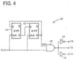
- FIG. 4 shows a specific example of a high-order-comparator control circuit 10.
- the high-order-comparator control circuit 10 includes two D-type flip-flops 11 and 13 clock signal terminals (CLK) of which receive inputs of clock signals CLK.
- a positive output terminal (Q) of the D-type flip-flop 11 is connected to an input terminal (D) of the D-type flip-flop 13 and a positive output terminal (Q) of the D-type flip-flop 13 is feedback to an input terminal (D) of the D-type flip-flop 11, whereby a dividing circuit is constituted.
- a divided signal DC1 from an output terminal (Q) and a clock signal CLK are inputted to a NAND gate 15 and then, a control signal 1B, a resultant signal of the above two signals, is outputted from there. Furthermore, the control signal 1B is inversed at inverter gates 17 and 19 and controls signals 1A and 1C are outputted from the inverter gates 17 and 19, respectively.
- FIG. 5 shows operational waveforms of high-order-comparator control circuit 10.
- the dividing circuit constituted by the two D-type flip-flops 11 and 13
- logic level of an output signal DC1 makes transition along with rising edge of clock signal and there can be generated a divided signal cycle length of which is double of a clock signal CLK.
- control signal 1B in high logic level is outputted while the two signals CLK and DC1 are in high logic level.
- Control signals 1A and 1C are outputted as inversion signal of a control signal 1B.
- Control signals 1A, 1B, and 1C control the switches SWA, SWB, and SWC (see FIG.
- each control signal (1A, 1B, 1C) shows a state of (high, low, high) during fetch operation (I) , and a state of (low, high, low) during voltage comparison operation (III).
- the high-order comparators COMP11, 12 and 13 are controlled under (1/2)-clock cycle state (I) and subsequent (3/2)-clock cycle state.
- FIG. 6 shows a specific example of a low-order-comparator control circuit 20.
- the low-order-comparator control circuit 20 includes a NOR gate 21 to which a divided signal DC2 and a clock signal CLK are inputted.
- a control signal 2B is outputted from the NOR gate 21.
- control signals 2A and 2C are outputted from inverter gates 17 and 19, respectively.
- FIG. 7 shows operational waveforms of the low-order-comparator control circuit 20.
- Control signals 2A and 2C are outputted as logic signal similar to the control signals 1A and 1C. Since a control signal 2B is an output signal from the NOR gate 21, a control signal 2B in high logic level is outputted while both a clock signal CLK and a divided signal DC2 are in low logic level.
- the low-order comparators COMP21, 22, and 23 has circuit structure such as FIG. 2, control signals 2A, 2B, and 2C control the switches SWA, SWB, and SWC, respectively, to set the switches conductive state ("ON") under high logic level condition.
- the low-order comparators COMP21, 22, and 23 are control under (1/2)-clock cycle state (I), (2/2)-clock cycle state (III) .
- FIG. 8 shows operational waveforms of the A/D converter of FIG. 1. Similar to the case of the previously-considered A/D converter of FIG. 11, comparators operate in synchronous with clock signals CLK. A (1/2)-clock cycle corresponds to a unit of time step. Here, A/D conversion operation is conducted taking time step 1 ⁇ through 5 ⁇ as one unit. Operation state during (I), (II), and (III) with respect to the high-order comparators COMP1x and the low-order comparators COMP2x are similar to the case or the prior art.
- the first switched SW11A, SW12A, and SW13A are set conductive state at time step 1 ⁇ -2 ⁇ where fetch operation (I) is conducted to fetch analog input voltage VAIN to the high-order comparators COMP1x and the low-order comparators COMP2x. Consequently, high-order reference voltages VN1, VN2, and VN3 are supplied to the voltage holding capacitance elements C11, C12, and C13, respectively.
- FIG. 8 shows a case that analog input voltage VAIN was voltage level VN1X which is same as or higher than high-order reference voltage VN2 and lower than high-order reference voltage VN1, in the precedent operation cycle.
- FIG. 8 shows a case that this phenomenon occurs to low-order voltage VN01, as an example. Since the reference voltage terminal (REF) of the high-order comparator COMP11 is not charged or discharged up to high-order reference voltage VN1 during voltage comparison operation (III) , a capacitance value of the voltage holding capacitance element C11 may be small. Furthermore, since quantity of electric charges to be replenished is a few, amount of peak-voltage fluctuation V1 can be set small. Accordingly, electric charges can be fully replenished to the voltage holding capacitance element C11 during time step 1 ⁇ -2 ⁇ . That is, recovery from voltage fluctuation of the low-order reference voltage VN01 at the ladder-resistance-element array, caused by charge replenishment, can be fully made during the time step 1 ⁇ -2 ⁇ .
- the high-order comparator COMP 11 shifts to comparison state (operation (III) ).
- voltage comparison operation is conducted by voltage transition due to charge distribution between the voltage-comparison capacitance element C0 or the like charged up to analog input voltage VAIN and the voltage-holding capacitance element C11 voltage level at which is charged up to the high-order reference voltage VN1. Accordingly, there is no need to charge or discharge voltage level of the reference voltage terminal (REF) at the high-order comparator COMP11 up to high-order reference voltage VN1. Therefore, outflow current from the reference voltage terminal (REF) at the high-order comparator COMP11 is significantly small peak current I1. This peak current I1 is smaller than the peak current I100 (FIG. 11) in the previously-considered circuitry and able to get rid of outflow current during time step 2 ⁇ -3 ⁇ .
- voltage level of the terminal voltage VC11 at the voltage-holding capacitance element C11 is higher than the high-order reference voltage VN1 as set value, due to charge distribution of voltage comparison operation (III) . Redundant charges corresponding to a voltage value that rises from the high-order reference voltage VN1 are discharged after time 5 ⁇ , the next operation cycle. Peak-voltage-fluctuation amount V1 at this stage is a small value, too. Therefore, voltage fluctuation can be cleared within the time step 2 ⁇ -3 ⁇ .
- the high-order reference voltages VN1, VN2, and VN3 are supplied from the ladder-resistance-element array during time step 2 ⁇ -3 ⁇ .
- the high-order reference voltages VN1, VN2, and VN3 can be supplied from the ladder-resistance-element array during time step 1 ⁇ -2 ⁇ , prior to time step 2 ⁇ -3 ⁇ , because the voltage-holding capacitance elements C11, C12, and C13 are provided therein.
- the high-order comparators COMP12, and COMF13 conducts comparison operation in a same manner as the high-order comparator COMP11.
- terminals voltages VC12, VC13 at the voltage holding capacitance elements C12, C13, outflow current from each of the reference voltage terminals (REF) of the high-order comparators COMP12 and COMP13, and voltage fluctuation of the low-order reference voltages VN02 and VN03 or the like are in same manners as the above.
- FIG. 9 show a conversion table of the A/D converter directed to FIG. 1.
- the analog-input voltage VAIN is divided in to sixteen voltage ranges by the ladder-resistance-element array and the sixteen voltage ranges are roughly divided into four by each of the high-order comparators COMP1x.
- Output signals O11, O12, and O13 from the high-order comparators COMP1x are encoded to generate high-order-two-bit digital codes.
- the switch control signals S1 through S4 are controlled. Based on these switch control signals S1 through S4, one of the change-over switch groups SW1 through SW4 is selected and voltage comparison operation is conducted at each of the low-order comparators COMP2x.
- the analog-input voltage VAIN divided into four is further divided into four.
- Output signals O21, O22, and O23 from the low-order comparators COMP2x are encoded to generate low-order-two-bit digital codes.
- the high-order reference voltages VN1, VN2 and VN3 are supplied from the voltage-divided terminals N1, N2, and N3 of the ladder-resistance-element array, as high-order voltage divided terminals of resistance-component-element array, to the voltage holding capacitance elements C11, C12, and C13, respectively.
- the high-order reference voltages VN1, VN2, and VN3 to be supplied to the high-order comparators COMP11, COMP12, and COMP13 as high-order-bit discrimination voltage comparator can be supplied from the voltage holding capacitance elements C11, C12, and C13.
- low-order reference voltages can be supplied without influences of voltage fluctuation at the voltage-divided terminals N1, N2, and N3, which occurs when the high-order reference voltages VN1, VN2, and VN3 are supplied to the voltage-holding capacitance elements C11, C12, and C13 from the voltage-divided terminals N1, N2, and N3, respectively.
- supply operation of the high-order reference voltage VN1, VN2, and VN3 to the voltage-holding capacitance elements C11, C12, and C13, respectively can be conducted temporarily apart from A/D conversion for low-order bits. Therefore, there never remains influence of voltage fluctuation at the voltage-divided terminals N1, N2, and N3 of the ladder-resistance-element array, which is due to supply operation the high-order reference voltages VN1, VN2, and VN3 to the voltage-holding capacitance elements C11, C12, and C13, until beginning of A/D conversion for low-order bits.
- the chopper-type comparators of the present embodiment can conduct voltage comparison operation when width of voltage transition at one terminal of a voltage-comparison capacitance element C0 reaches same as or higher than a predetermined voltage value.
- This predetermined voltage value may be a small voltage value because the inverter gate INV can detect the voltage. Accordingly, when the high-order reference voltage VN1, VN2, and VN3 are supplied for comparison operation, it is not necessary to charge or discharge voltage at one end of the voltage-comparison capacitance element C0 up to level of the high-order reference voltages VN1, VN2, and VN3.
- the voltage-holding capacitance elements C11, C12, and C13 may have capacitance values that are large enough to cause voltage transition of the predetermined voltage value by charge distribution between the voltage-comparison capacitance element C0 and the voltage-holding capacitance elements C11, C12, and C13. Amount of charges consumed at the voltage-holding capacitance elements C11, C12, and C13 may be few compared with the case that voltage at one terminal of the voltage-comparison capacitance element C0 is charged or discharged up to level of the high-order reference voltages VN1, VN2, and VN3.
- conductivity of the first switches SW11A, SW12A, and SW13A and the second switches SW11B, SW12B, and SW13B is controlled.
- the high-order reference voltages VN1, VN2 and VN3 can be supplied to the voltage-holding capacitance elements C11, C12, and C13, as well as, to the high-order comparators COMP11, COMP12, and COMP13, respectively.
- control signals 1C, 1B used for A/D conversion operation at the high-order comparators COMP11, COMP12, and COMP13 conductivity of the voltage-holding capacitance elements C11, C12, and C13 can be controlled.
- high-order reference voltages VN1, VN2 and VN3 are supplied to the voltage-holding capacitance elements C11, C12, and C13 while high and low-order reference voltages required for A/D conversion operation of high-order bits and low-order bits are generated at the ladder-resistance-element array. Accordingly, current flowing through the ladder-resistance-element array when the high-order reference voltages VN1, VN2 and VN3 can be supplied to the voltage-holding capacitance elements in asynchronous with A/D conversion operation for low-order bit. Accordingly, voltage fluctuation of low-order reference voltages does not remain at the time to A/D conversion for low-order bits.
- the present embodiment describes a case that the reference terminals of the voltage-holding capacitance elements C11, C12, and C13 are connected to ground voltage.
- the reference terminals may be connected to the terminals (RH) for supplying maximum reference voltage VRH, the terminals (RL) for supplying minimum reference voltage VRL, or power source voltage VCC of the A/D converter.
- the present embodiment describes a case of a series-parallel A/D converter.
- type of A/D converter is not limited to series-parallel type.
- the aspects of the present invention are applicable to other types of A/D converter, not to mention.
- reference voltage generated at the ladder-resistance-element array is firstly charged to the voltage holding capacitance element. After that, the ladder-resistance-element array is separated from the voltage holding capacitance element and voltage comparison is conducted at a comparator. Accordingly, influence due to voltage comparison does not propagate to the ladder-resistance-element array.
- transitional fluctuation of reference voltage due to comparison operation by high-order comparators does not remain until comparison operation by low-order comparators begins. Accordingly, low-order reference voltage does not fluctuate when voltage comparison operation begins. Since there is no need to await calm down of voltage fluctuation of reference voltage before comparison operation at the low-order comparator, high-speed operation of an A/D converter circuit can be realized.
Landscapes
- Engineering & Computer Science (AREA)
- Theoretical Computer Science (AREA)
- Analogue/Digital Conversion (AREA)
Abstract
Description
Claims (13)
- An A/D converter circuit comprising:wherein the A/D converter circuit further includes reference voltage holding section(s) for holding the respective reference voltage(s) supplied from each voltage-divided terminal and supplies' the respective reference voltage(s) held thereat to the respective voltage comparator(s) after each of the voltage-divided terminal(s) is electrically separated from the respective reference voltage holding section(s).one or more voltage comparators for conducting A/D conversion; anda resistance-component-element array for generating respective reference voltage(s) for the respective voltage comparator(s) at each voltage-divided terminal of the resistance-component-element array;
- An A/D converter circuit comprising:wherein the A/D converter circuit further includes each reference voltage holding section for holding each high-order reference voltage supplied from each high-order voltage-divided terminal and supplies each high-order reference voltage held thereat to each high-order-bit-discrimination voltage comparator after each high-order-voltage-divided terminal is electrically separated from the each reference voltage holding section.one or more high-order-bit-discrimination voltage comparators for conducting A/D conversion of high-order bits prior to A/D conversion of low-order bits; anda resistance-component-element array for generating each high-order reference voltage for A/D conversion of each of the high-order bits at each high-order-voltage-divided terminal, and each low-order reference voltage for A/D conversion of each of the low-order bits at each low-order-voltage-divided terminal, the resistance-component-element array being connected between high-voltage-side reference voltage and low-voltage-side reference voltage;
- An A/D converter circuit according to claim 2, wherein supply of the high-order reference voltage to the reference voltage holding section from the high-order-voltage-divided terminal and supply of the low-order reference voltage to the reference voltage holding section from the low-order-voltage-divided terminal are conducted with different timing.
- An A/D converter circuit according to claim 2, wherein supply of the high-order reference voltage to the reference voltage holding section from the high-order-voltage-divided terminal completes before supply of the low-order reference voltage to the reference voltage holding section from the low-order-voltage-divided terminal starts.
- An A/D converter circuit according to claim 2, wherein supply of the high-order reference voltage to the reference voltage holding section from the high-order-voltage-divided terminal is conducted concurrently with fetch of input voltage to the high-order-bit-discrimination voltage comparator.
- An A/D converter circuit according to claim 5, wherein the high-order-bit-discrimination voltage comparator is chopper-type voltage comparator including a voltage-comparison capacitance element, and voltage comparison operation is conducted in a manner that firstly the input voltage is fetched to one end of the voltage-comparison capacitance element and subsequently the high-order reference voltage is fetched to another end of the voltage-comparison capacitance element, and finally the two kinds of voltages are compared.
- An A/D converter circuit according to claim 6, wherein the reference voltage holding section includes a voltage-holding capacitance element, and the voltage comparison operation is conducted by detecting voltage transition from level of the input voltage at one terminal of the voltage-comparison capacitance element, the voltage transition occurring when the high-order reference voltage is fetched to the high-order-bit-discrimination voltage comparator(s) and electric charge is re-distributed between the voltage-comparison capacitance element and the voltage-holding capacitance element.
- An A/D converter circuit according to claim 2, wherein the reference voltage holding section includes a voltage-holding capacitance element, and the A/D converter circuit further includes a first switching section for controlling connection between the voltage-holding capacitance element and the high-order-voltage-divided terminal, and a second switching section for controlling connection between the voltage-holding capacitance element and the high-order-bit-discrimination voltage comparator.
- An A/D converter circuit according to claim 2, wherein the resistance-component-element array is a ladder-resistance-element array for generating voltage divided responding to a number of output bits obtained after A/D conversion, voltage divided terminals between resistance elements constituting the ladder-resistance-element array are arranged as the high-order-voltage-divided terminal for every predetermined number of voltage-divided terminal set as the low-order-voltage-divided terminals, and current is supplied through the ladder-resistance-element array when the high-order reference voltage is supplied to the reference voltage holding section.
- An A/D converter circuit according to claim 8, wherein connection control by the first switching section and connection control by the second switching are conducted with different timing.
- An A/D converter circuit according to claim 8, wherein connection of the first switching section completes before supply of the low-order reference voltage to the reference voltage holding section from the low-order-voltage-divided terminal starts.
- An A/D converter circuit according to claim 8, wherein connection of the first switching section is conducted concurrently with fetch of input voltage to the high-order-bit-discrimination voltage comparator.
- An A/D converter circuit according to claim 8, wherein the resistance-component-element array is a ladder-resistance-element array for generating voltage divided responding to a number of output bits obtained after A/D conversion, voltage divided terminals between resistance elements constituting the ladder-resistance-element array are arranged as the high-order-voltage-divided terminal for every predetermined number of voltage-divided terminal set as the low-order-voltage-divided terminals, and current is supplied through the ladder-resistance-element array when the high-order reference voltage is supplied to the reference voltage holding section.
Applications Claiming Priority (2)
| Application Number | Priority Date | Filing Date | Title |
|---|---|---|---|
| JP2002093878A JP3968261B2 (en) | 2002-03-29 | 2002-03-29 | A / D conversion circuit |
| JP2002093878 | 2002-03-29 |
Publications (3)
| Publication Number | Publication Date |
|---|---|
| EP1349283A2 true EP1349283A2 (en) | 2003-10-01 |
| EP1349283A3 EP1349283A3 (en) | 2004-05-06 |
| EP1349283B1 EP1349283B1 (en) | 2005-12-28 |
Family
ID=27800537
Family Applications (1)
| Application Number | Title | Priority Date | Filing Date |
|---|---|---|---|
| EP02256878A Expired - Lifetime EP1349283B1 (en) | 2002-03-29 | 2002-10-03 | A/D converter circuit |
Country Status (7)
| Country | Link |
|---|---|
| US (1) | US6707412B2 (en) |
| EP (1) | EP1349283B1 (en) |
| JP (1) | JP3968261B2 (en) |
| KR (1) | KR100902812B1 (en) |
| CN (1) | CN1326329C (en) |
| DE (1) | DE60208331T2 (en) |
| TW (1) | TW566007B (en) |
Families Citing this family (8)
| Publication number | Priority date | Publication date | Assignee | Title |
|---|---|---|---|---|
| EP1367720B1 (en) * | 2002-05-27 | 2007-06-13 | Fujitsu Limited | A/D converter bias current circuit |
| JP2005142932A (en) * | 2003-11-07 | 2005-06-02 | Sanyo Electric Co Ltd | Ad converter |
| KR101256001B1 (en) * | 2004-07-08 | 2013-04-18 | 오끼 덴끼 고오교 가부시끼가이샤 | Driving circuit of the liquid crystal display device |
| US7782234B2 (en) * | 2007-05-31 | 2010-08-24 | Analog Devices, Inc. | Successive approximation analog-to-digital converter with inbuilt redundancy |
| CN101499801B (en) * | 2008-01-31 | 2011-09-14 | 凯迈(洛阳)测控有限公司 | A/D conversion circuit and conversion method thereof |
| CN101547000B (en) * | 2009-05-08 | 2011-05-04 | 炬力集成电路设计有限公司 | A signal conversion circuit, digit-analog conversion device and audio frequency output equipment |
| CN102291147A (en) * | 2011-05-31 | 2011-12-21 | 深圳市博驰信电子有限责任公司 | Analog-digital conversion circuit, analog-digital converter and analog-digital conversion method |
| JP7085428B2 (en) * | 2018-07-10 | 2022-06-16 | 株式会社半導体エネルギー研究所 | Battery protection circuit, power storage device, and electrical equipment |
Family Cites Families (16)
| Publication number | Priority date | Publication date | Assignee | Title |
|---|---|---|---|---|
| US4745393A (en) * | 1985-09-25 | 1988-05-17 | Hitachi, Ltd | Analog-to-digital converter |
| JPS62258521A (en) | 1986-05-02 | 1987-11-11 | Nec Corp | Analog-digital converter |
| JPH01106527A (en) * | 1987-10-19 | 1989-04-24 | Mitsubishi Electric Corp | Ad converter |
| JPH0522136A (en) * | 1990-11-16 | 1993-01-29 | Hitachi Ltd | Analog / Digital converter |
| JPH05218868A (en) * | 1992-02-03 | 1993-08-27 | Hitachi Ltd | Multistage a/d converter |
| JP3103657B2 (en) * | 1992-03-23 | 2000-10-30 | 松下電器産業株式会社 | A / D converter having voltage holding circuit and capacitive coupling network |
| US5675340A (en) * | 1995-04-07 | 1997-10-07 | Iowa State University Research Foundation, Inc. | Charge-redistribution analog-to-digital converter with reduced comparator-hysteresis effects |
| JP3709640B2 (en) * | 1996-12-27 | 2005-10-26 | ソニー株式会社 | Voltage comparison circuit and analog / digital conversion circuit using the same |
| IES80452B2 (en) * | 1997-01-22 | 1998-07-29 | Univ Cork | Reduction of comparator power requirement in a switched capacitor adc |
| US5861829A (en) * | 1997-04-28 | 1999-01-19 | Marvell Technology Group, Ltd. | High-speed, low power, medium resolution analog-to-digital converter and method of stabilization |
| JP3439322B2 (en) * | 1997-06-17 | 2003-08-25 | Necエレクトロニクス株式会社 | Differential input chopper type voltage comparison circuit |
| JP3621249B2 (en) * | 1998-02-27 | 2005-02-16 | 富士通株式会社 | Voltage selection circuit, LCD drive circuit, and D / A converter |
| KR100311043B1 (en) * | 1999-08-05 | 2002-01-19 | 윤종용 | Digital-to-analog converter capable of fast switching and precision voltage conversion |
| US6411233B1 (en) * | 2000-06-06 | 2002-06-25 | Marvell International Ltd | Method and apparatus for direct RAM analog-to-digital converter calibration |
| US6456220B1 (en) * | 2000-06-19 | 2002-09-24 | Cygnal Integrated Products, Inc. | Analog-to-digital converter for processing differential and single-ended inputs |
| KR100342396B1 (en) * | 2000-07-31 | 2002-07-02 | 황인길 | Folding analog to digital convertor |
-
2002
- 2002-03-29 JP JP2002093878A patent/JP3968261B2/en not_active Expired - Fee Related
- 2002-10-02 US US10/261,674 patent/US6707412B2/en not_active Expired - Lifetime
- 2002-10-03 EP EP02256878A patent/EP1349283B1/en not_active Expired - Lifetime
- 2002-10-03 DE DE60208331T patent/DE60208331T2/en not_active Expired - Fee Related
- 2002-10-11 TW TW091123501A patent/TW566007B/en not_active IP Right Cessation
- 2002-10-16 KR KR1020020063117A patent/KR100902812B1/en not_active Expired - Fee Related
- 2002-11-07 CN CNB021502692A patent/CN1326329C/en not_active Expired - Fee Related
Also Published As
| Publication number | Publication date |
|---|---|
| JP3968261B2 (en) | 2007-08-29 |
| KR20030078610A (en) | 2003-10-08 |
| TW566007B (en) | 2003-12-11 |
| KR100902812B1 (en) | 2009-06-12 |
| US20030184465A1 (en) | 2003-10-02 |
| EP1349283B1 (en) | 2005-12-28 |
| US6707412B2 (en) | 2004-03-16 |
| DE60208331D1 (en) | 2006-02-02 |
| CN1449118A (en) | 2003-10-15 |
| JP2003298421A (en) | 2003-10-17 |
| EP1349283A3 (en) | 2004-05-06 |
| CN1326329C (en) | 2007-07-11 |
| DE60208331T2 (en) | 2006-06-29 |
Similar Documents
| Publication | Publication Date | Title |
|---|---|---|
| US7265707B2 (en) | Successive approximation type A/D converter | |
| EP1349283B1 (en) | A/D converter circuit | |
| CN113014264A (en) | Analog-digital converter with multi-mode selection | |
| KR100708939B1 (en) | Digital / Analog Converter | |
| US6218975B1 (en) | Interleaved auto-zero analog-to-digital converter with switching noise compensation | |
| US5329172A (en) | Chopping type comparator with clocked inverter | |
| US6927723B2 (en) | A/D converter and A/D conversion method | |
| KR0172206B1 (en) | Solid catalyst for etherification reaction and preparation of ether compound using the same | |
| JP2780992B2 (en) | Error-correcting electronics suitable for thermometer or circular code | |
| US6847322B2 (en) | Sequential comparison type AD converter and microcomputer | |
| JP2005142932A (en) | Ad converter | |
| JP3992830B2 (en) | A / D converter | |
| US20070229341A1 (en) | Successive approximation A/D converter comparing analog input voltage to reference voltages | |
| US6590514B2 (en) | D/A converter circuit | |
| CN214675121U (en) | A multi-mode selection analog-to-digital converter | |
| EP3696983A1 (en) | Analog to digital converter | |
| US6822599B2 (en) | Integrated circuit and A/D conversion circuit | |
| US12556194B2 (en) | Successive approximation ad converter circuit | |
| JPH11340830A (en) | Successive comparison a/d converter circuit | |
| JP3382818B2 (en) | Test circuit for D / A converter | |
| JP2024055267A (en) | Successive-approximation type a/d conversion circuit | |
| JPH1013230A (en) | Analog-to-digital converter | |
| JPH07123004A (en) | A-D conversion circuit | |
| JP2007259224A (en) | Successive approximation AD converter | |
| IT9021863A1 (en) | TWO-CONVERSION ANALOG / DIGITAL CONVERTER. |
Legal Events
| Date | Code | Title | Description |
|---|---|---|---|
| PUAI | Public reference made under article 153(3) epc to a published international application that has entered the european phase |
Free format text: ORIGINAL CODE: 0009012 |
|
| AK | Designated contracting states |
Kind code of ref document: A2 Designated state(s): AT BE BG CH CY CZ DE DK EE ES FI FR GB GR IE IT LI LU MC NL PT SE SK TR |
|
| AX | Request for extension of the european patent |
Extension state: AL LT LV MK RO SI |
|
| PUAL | Search report despatched |
Free format text: ORIGINAL CODE: 0009013 |
|
| AK | Designated contracting states |
Kind code of ref document: A3 Designated state(s): AT BE BG CH CY CZ DE DK EE ES FI FR GB GR IE IT LI LU MC NL PT SE SK TR |
|
| AX | Request for extension of the european patent |
Extension state: AL LT LV MK RO SI |
|
| RIC1 | Information provided on ipc code assigned before grant |
Ipc: 7H 03M 1/14 A Ipc: 7H 03M 1/36 B |
|
| 17P | Request for examination filed |
Effective date: 20040714 |
|
| 17Q | First examination report despatched |
Effective date: 20040908 |
|
| AKX | Designation fees paid |
Designated state(s): DE FR GB |
|
| GRAP | Despatch of communication of intention to grant a patent |
Free format text: ORIGINAL CODE: EPIDOSNIGR1 |
|
| GRAP | Despatch of communication of intention to grant a patent |
Free format text: ORIGINAL CODE: EPIDOSNIGR1 |
|
| GRAS | Grant fee paid |
Free format text: ORIGINAL CODE: EPIDOSNIGR3 |
|
| GRAA | (expected) grant |
Free format text: ORIGINAL CODE: 0009210 |
|
| AK | Designated contracting states |
Kind code of ref document: B1 Designated state(s): DE FR GB |
|
| REG | Reference to a national code |
Ref country code: GB Ref legal event code: FG4D |
|
| REF | Corresponds to: |
Ref document number: 60208331 Country of ref document: DE Date of ref document: 20060202 Kind code of ref document: P |
|
| ET | Fr: translation filed | ||
| PLBE | No opposition filed within time limit |
Free format text: ORIGINAL CODE: 0009261 |
|
| STAA | Information on the status of an ep patent application or granted ep patent |
Free format text: STATUS: NO OPPOSITION FILED WITHIN TIME LIMIT |
|
| 26N | No opposition filed |
Effective date: 20060929 |
|
| REG | Reference to a national code |
Ref country code: GB Ref legal event code: 732E |
|
| PGFP | Annual fee paid to national office [announced via postgrant information from national office to epo] |
Ref country code: DE Payment date: 20081014 Year of fee payment: 7 |
|
| PGFP | Annual fee paid to national office [announced via postgrant information from national office to epo] |
Ref country code: FR Payment date: 20081014 Year of fee payment: 7 |
|
| REG | Reference to a national code |
Ref country code: FR Ref legal event code: TP |
|
| PGFP | Annual fee paid to national office [announced via postgrant information from national office to epo] |
Ref country code: GB Payment date: 20081001 Year of fee payment: 7 |
|
| REG | Reference to a national code |
Ref country code: FR Ref legal event code: ST Effective date: 20100630 |
|
| PG25 | Lapsed in a contracting state [announced via postgrant information from national office to epo] |
Ref country code: DE Free format text: LAPSE BECAUSE OF NON-PAYMENT OF DUE FEES Effective date: 20100501 Ref country code: FR Free format text: LAPSE BECAUSE OF NON-PAYMENT OF DUE FEES Effective date: 20091102 |
|
| PG25 | Lapsed in a contracting state [announced via postgrant information from national office to epo] |
Ref country code: GB Free format text: LAPSE BECAUSE OF NON-PAYMENT OF DUE FEES Effective date: 20091003 |