EP1349276A2 - Semiconductor integrated circuit - Google Patents
Semiconductor integrated circuit Download PDFInfo
- Publication number
- EP1349276A2 EP1349276A2 EP03090082A EP03090082A EP1349276A2 EP 1349276 A2 EP1349276 A2 EP 1349276A2 EP 03090082 A EP03090082 A EP 03090082A EP 03090082 A EP03090082 A EP 03090082A EP 1349276 A2 EP1349276 A2 EP 1349276A2
- Authority
- EP
- European Patent Office
- Prior art keywords
- oscillation
- waveform shaping
- gnd
- section
- circuit
- Prior art date
- Legal status (The legal status is an assumption and is not a legal conclusion. Google has not performed a legal analysis and makes no representation as to the accuracy of the status listed.)
- Withdrawn
Links
Images




Classifications
-
- H—ELECTRICITY
- H03—ELECTRONIC CIRCUITRY
- H03K—PULSE TECHNIQUE
- H03K5/00—Manipulating of pulses not covered by one of the other main groups of this subclass
- H03K5/01—Shaping pulses
- H03K5/08—Shaping pulses by limiting; by thresholding; by slicing, i.e. combined limiting and thresholding
-
- H—ELECTRICITY
- H03—ELECTRONIC CIRCUITRY
- H03K—PULSE TECHNIQUE
- H03K3/00—Circuits for generating electric pulses; Monostable, bistable or multistable circuits
- H03K3/02—Generators characterised by the type of circuit or by the means used for producing pulses
- H03K3/027—Generators characterised by the type of circuit or by the means used for producing pulses by the use of logic circuits, with internal or external positive feedback
- H03K3/03—Astable circuits
- H03K3/0307—Stabilisation of output, e.g. using crystal
-
- H—ELECTRICITY
- H03—ELECTRONIC CIRCUITRY
- H03K—PULSE TECHNIQUE
- H03K3/00—Circuits for generating electric pulses; Monostable, bistable or multistable circuits
- H03K3/01—Details
- H03K3/013—Modifications of generator to prevent operation by noise or interference
Definitions
- the invention relates to semiconductor integrated circuits, and more particularly to a semiconductor integrated circuit containing an oscillator and reducing Electro-Magnetic interference (hereinafter, abbreviated to EMI) noise produced by the oscillator.
- EMI Electro-Magnetic interference
- EMI noise caused by an oscillator integrated in the above described semiconductor integrated circuit is always emitted in almost all the operating modes thereof except when the oscillator is in a standby mode to be stopped. Therefore, the reduction of noise caused by the oscillator is one of the challenges for the reduction of EMI noise.
- a semiconductor integrated circuit containing such a conventional oscillator is disclosed, for example, in Japanese Patent Laid-Open No. 02-228106.
- FIG. 1 is a block diagram of a semiconductor integrated circuit containing a conventional oscillator.
- a semiconductor integrated circuit 900 containing a conventional oscillator an output A1 from an oscillating section 910 is input to a waveform shaping section 920 including a Schmitt circuit S8, and an output signal 925 is output via an output buffer BUF 5.
- the Schmitt circuit S8 is inserted for the purpose of blocking noise superimposed on output from the oscillating section 910, and it serves to increase Electro-Magnetic susceptibility (hereinafter, abbreviated to EMS) characteristic.
- EMS Electro-Magnetic susceptibility
- the Schmitt circuit serves to reduce EMI noise caused by through-current by eliminating changes in its state in the case in which the output A1 from the key oscillating section 910 is at the intermediate potential.
- FIG. 2 shows the results of Fast Fourier transform (hereinafter, abbreviated to FFT) analyses of an oscillation power-source current Ivddosc flowing through the oscillation circuit and a waveform-shaping section power-source current Ivdd flowing through the waveform shaping section including the Schmitt circuit when the semiconductor integrated circuit containing the conventional oscillator shown in FIG. 1 is in stable oscillation.
- FFT Fast Fourier transform
- FIG. 3 shows current waveforms at that time.
- the oscillation power-source current Ivddosc flowing through the oscillation circuit in stable oscillation has a peak at the oscillation frequency of a point P, and the spectra fall downward with increasing frequency.
- transistor element P13 and N13 are constantly switched according to feedback signals, and their through-current also complicatedly change with changes in gm of the transistor elements . Because a signal with a rectangular waveform shaped by the Schmitt circuit S8 is input to the output buffer (BUF5) connected to the following stage, the through-current of the buffer becomes steep. Therefore, the waveform-shaping section power-source current Ivdd flowing through the waveform shaping section becomes steep and complicated, as shown in the waveform-shaping section power-source current Ivdd of FIG. 3, and thus its spectra spreads to the high frequency region.
- semiconductor integrated circuits containing the conventional oscillator as described above are further disclosed in Japanese Patent Laid-Open No. 02-174248 and Japanese Patent Laid-Open No. 11-145727.
- a typical, known method is to insert a pass capacitor near a noise source.
- insertion of a pass capacitor in the vicinity of the oscillator is not so effective for the reduction of noise produced by the waveform shaping section including the Schmitt circuit since the capacitor is mostly used for charging and discharging of the feedback inverter within the oscillating section, as shown for the oscillation power-source current Ivddosc in FIG. 3.
- An object of the invention is to provide a semiconductor integrated circuit reducing EMI noise produced by an oscillator by dividing the oscillator into an oscillating section and a waveform shaping section.
- the supplies of power are separated and the supply of power to the waveform shaping section is performed through a dedicated low pass filter, and a stable-oscillation state signal is used to control a high frequency noise source within the waveform shaping section after the oscillation becomes stable.
- the waveform shaping section of the semiconductor integrated circuit according to the invention includes a Schmitt circuit which has a hysteresis characteristic during the unstable period of the oscillating section in the course of oscillation growth from the start of oscillation, and which operates as a buffer circuit when the oscillating section is in the state of stable oscillation.
- the Schmitt circuit of the semiconductor integrated circuit according to the invention has a first transistor element and a second transistor element, and during the unstable period of the oscillating section in the course of oscillation growth from the start of oscillation, the first transistor element and the second transistor element receive a feedback signal in a positive phase and the Schmitt circuit has a hysteresis characteristic.
- the first transistor element and the second transistor element each change into the OFF state and the Schmitt circuit becomes a buffer circuit.
- the invention is characterized in that, for dealing with EMI noise produced by an oscillator, which noise has been a problem with the prior art, the oscillator is divided into an oscillating section and a waveform shaping section and the supplies of power to their sections are separated, thus providing the supply of power to the waveform shaping section through a dedicated low path filter, and further a stable-oscillation state signal is used to control a high frequency noise source within the waveform shaping section after the oscillation becomes stable.
- the built-in oscillation circuit comprises an oscillating section 110 consisting of a feedback inverter INV1 and a feedback resistor R2, and a waveform shaping section 120.
- the supplies of power are separately provided to the oscillating section 110 and waveform shaping section 120, respectively. That is, referring to FIG. 4B, the supply of power to the waveform shaping section 120 is provided through a low pass filter 111 comprised of a resistor R1 and a capacitor C1, wherein a high potential power source VDD is supplied to the waveform shaping section as a high potential power source VDDX.
- transistor element P3 and N3 of a Schmitt circuit S1 in the waveform shaping section 120 are respectively connected to receive, as the respective gate control signals, signals Gp3 and Gn3 produced by a stable-oscillation signal A1 and logic elements AND1, OR1, and INV3.
- the output of a stable-oscillation timer and the like is used as the stable-oscillation signal A1.
- the power source of the waveform shaping section 120 in the first circuit 100 is connected to the waveform shaping section 120 through the low pass filter 111.
- the supply of power to the waveform shaping section 120 is separated from the oscillating section 110, and the capacitor C1 can serve effectively for the waveform shaping section 110 because the resistor R1 disposed between the waveform shaping section 120 and the oscillating section 110 limits the discharging current of the capacitor C1 to the oscillating section 110, which consumes a large amount of current.
- the capacitor C1 only requires a small value of capacitance. That is, by the separation of power source supplied to both sections and the insertion of a resistor between both sections, it becomes possible that a small amount of apacitance reduces the sneaking amount of high frequency noise produced by the waveform shaping section into the power source line.
- a feedback signal F1 is transmitted in a positive phase to the transistor elements P3 and N3 and the Schmitt circuit S1 operates as a normal Schmitt circuit having a hysteresis characteristic.
- the oscillator 110 goes into the state of stable oscillation and the stable-oscillation signal then becomes High, the gate signal Gp3 to the transistor element P3 becomes HIGH and the gate signal Gn3 to the transistor element N3 becomes LOW, thereby causing the transistors P3 and N3 each to be in the state of OFF.
- the Schmitt circuit S1 operates as a normal buffer not having a hysteresis characteristic.
- the transistor elements P3 and N3 go OFF, whereby the waveform of through-current flowing through the Schmitt circuit S1 becomes low in its peak value and also becomes simple in its waveform, thereby reducing high frequency power source noise caused by the Schmitt circuit.
- FIG. 7 a semiconductor integrated circuit according to a second embodiment of the invention will be described referring to FIG. 7.
- the circuit according to the second embodiment is different in that a stable-oscillation signal A2 acts to cause the Schmitt circuit to be bypassed since the oscillation became stable.
- the constituent elements except for those for this operation are the same as those of the circuit according to the first embodiment, and therefore detailed description thereof will be omitted.
- the input of the Schmitt circuit S1 is fixed to GND, thereby operating to eliminate the through-current flowing through the Schmitt circuit S1.
- the constituent elements of an inverter INV4 are in advance designed to be small in the current-driving ability, the through-current flowing through the whole of the waveform shaping section can be further decreased, and therefore it is possible to substantially suppress the production of high frequency noise.
- the circuit according to the first embodiment After the circuit according to the first embodiment reaches stable oscillation, it eliminates the hysteresis characteristic of the Schmitt circuit. In contrast to this, the third embodiment optimizes the hysteresis characteristic.
- the transistor elements P7 and N7 each go OFF, but the transistor elements P6 and N6 keep their hysteresis characteristics themselves because the output of an INV6 continues inputting thereto.
- the transistor elements P7 and N7 become OFF, the widths of hysteresis of the transistor elements P6 and N6 are narrower than those when the stable-oscillation signal A3 is LOW, but the production of high frequency noise can be suppressed by the corresponding amount.
- the effect of external noise input via the oscillating section 110 decreases because the output of the feedback inverter has an inductance component. Therefore, by suppressing to a required minimum the hysteresis width after the oscillation becomes stable, it possible to keep EMS characteristics while suppressing the production of high frequency noise.
- the semiconductor integrated circuit 500 according to the third embodiment is useful for a circuit in which importance is attached to the EMS characteristic.
- a transistor element N9 is in the state of OFF.
- the transistor elements P8 and N8 are designed such that the threshold value of BUF3 at this time may deviate from the central value of the output voltage X21 (621) of the oscillating section 110, as shown in the threshold value 711 of BUF3 of FIG. 10
- Deviation of the threshold value prevents a yet-to-be-grown signal X21 and external noise superimposed on a stable signal X21 from transmitting to the output of BUF4. Since the stable-oscillation signal became HIGH, a transistor element N9 has been in the ON state.
- the threshold value of BUF3 at this time to the central value of the output voltage X21 of the oscillating section 110, as shown in the threshold value 712 of BUF3 of FIG. 10, the duty ratio of the output of BUF 4 can be made 1:1.
- the semiconductor integrated circuit according to the fourth embodiment is useful for a semiconductor integrated circuit using original oscillation as-is without frequency dividing of the output of the oscillator.
- the semiconductor integrated circuit according to the first embodiment provides the low pass filter 111 inserted for the power source.
- a semiconductor integrated circuit 801 according to the fifth embodiment also separates the GND line to a waveform shaping section 120 and inserts a low pass filter 811 between GND and the wave form shaping section 120 via a resistor R4. In such a manner, the waveform shaping section 120 is given a potential via the low pass filter 811, thereby preventing high frequency noise produced by the waveform shaping section 120 from sneaking into the GND line located inside and outside the semiconductor chip.
- the separating of power source interconnection and the addition of a low pass filter can reduce the sneaking amount of high frequency power source noise caused by the oscillator waveform-shaping section into elements located inside and outside the semiconductor chip.
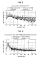
- FIG. 5 shows the results of the comparison of currents flowing through the Schmitt circuit S1 when the stable-oscillation signal 1 is LOW and when it is HIGH. It can be seen that when the stable-oscillation signal 1 becomes HIGH, the spectra in the high frequency region are decreased.
- FIG. 6 shows the results of the comparison of the sums of the oscillating section power-source current Ivddosc and the waveform shaping section power-source current Ivdd when the power source is separated and the low pass filter is inserted, as described in connection to the first embodiment, and when such measures are not taken.
- the capacitance C1 of FIG. 4B has the effect of decreasing the spectra of the high frequency region, because it can effectively act for the waveform shaping section without being used for the oscillating section 1.
Landscapes
- Chemical & Material Sciences (AREA)
- Crystallography & Structural Chemistry (AREA)
- Physics & Mathematics (AREA)
- Nonlinear Science (AREA)
- Inductance-Capacitance Distribution Constants And Capacitance-Resistance Oscillators (AREA)
- Oscillators With Electromechanical Resonators (AREA)
- Logic Circuits (AREA)
- Manipulation Of Pulses (AREA)
- Semiconductor Integrated Circuits (AREA)
Abstract
Description
Claims (14)
- A semiconductor integrated circuit comprising:an oscillating section supplied with a predetermined potential to oscillate;a waveform shaping section receiving the output of said oscillating section and controlling a high frequency noise source after the oscillation of said oscillating section has become stable, wherein the supply of power to said waveform shaping section is different from the supply of power to said oscillating section, and said supply of power to said waveform shaping section is provided through a low pass filter filtering to supply a predetermined potential thereto.
- The circuit according to claim 1, wherein said waveform shaping section includes a Schmitt circuit which has a hysteresis characteristic during the unstable period of said oscillating section in the course of oscillation growth from the start of oscillation, and which operates as a buffer circuit when said oscillating section is in the state of stable-oscillation.
- The circuit according to claim 2, wherein said Schmitt circuit has a first transistor element and a second transistor element, and during said unstable period in said course of oscillation growth from the start of oscillation, said first transistor element and said second transistor element receive a feedback signal in a positive phase and said Schmitt circuit has a hysteresis characteristic, and wherein when said oscillating section goes into the state of stable oscillation, said first transistor element and said second transistor element each change into the OFF state and said Schmitt circuit becomes a buffer circuit.
- The circuit according to claim 2, wherein when said oscillating section goes into the state of stable oscillation, the input of said Schmitt circuit is fixed to GND.
- The circuit according to claim 3, wherein when said oscillating section goes into the state of stable oscillation, the input of said Schmitt circuit is fixed to GND.
- The circuit according to claim 1, wherein said waveform shaping section includes a Schmitt circuit which has a hysteresis characteristic during the unstable period of said oscillating section in the course of oscillation growth from the start of oscillation, and which has a hysteresis characteristic narrower than the hysteresis width during said unstable period when said oscillating section goes into the state of stable-oscillation.
- The circuit according to claim 1, wherein said waveform shaping section comprises a buffer circuit with a first transistor element and a second transistor element, and the threshold value of said buffer circuit is set to deviate from the center value of the output voltage of said oscillating section during the unstable period of said oscillating section in the course of oscillation growth from the start of oscillation.
- The circuit according to claim 1, wherein the supply of GND to said waveform shaping section is performed through a low pass filter for filtering to give said GND thereto.
- The circuit according to claim 2, wherein the supply of GND to said waveform shaping section is performed through a low pass filter for filtering to give said GND thereto.
- The circuit according to claim 3, wherein the supply of GND to said waveform shaping section is performed through a low pass filter for filtering to give said GND thereto.
- The circuit according to claim 4, wherein the supply of GND to said waveform shaping section is performed through a low pass filter for filtering to give said GND thereto.
- The circuit according to claim 5, wherein the supply of GND to said waveform shaping section is performed through a low pass filter for filtering to give said GND thereto.
- The circuit according to claim 6, wherein the supply of GND to said waveform shaping section is performed through a low pass filter for filtering to give said GND thereto.
- The circuit according to claim 7, wherein the supply of GND to said waveform shaping section is performed through a low pass filter for filtering to give said GND thereto.
Applications Claiming Priority (2)
| Application Number | Priority Date | Filing Date | Title |
|---|---|---|---|
| JP2002089138 | 2002-03-27 | ||
| JP2002089138A JP3638564B2 (en) | 2002-03-27 | 2002-03-27 | Semiconductor integrated circuit |
Publications (2)
| Publication Number | Publication Date |
|---|---|
| EP1349276A2 true EP1349276A2 (en) | 2003-10-01 |
| EP1349276A3 EP1349276A3 (en) | 2005-10-12 |
Family
ID=27800484
Family Applications (1)
| Application Number | Title | Priority Date | Filing Date |
|---|---|---|---|
| EP03090082A Withdrawn EP1349276A3 (en) | 2002-03-27 | 2003-03-26 | Semiconductor integrated circuit |
Country Status (6)
| Country | Link |
|---|---|
| US (1) | US7106144B2 (en) |
| EP (1) | EP1349276A3 (en) |
| JP (1) | JP3638564B2 (en) |
| KR (1) | KR20030078039A (en) |
| CN (1) | CN1447521A (en) |
| TW (1) | TW200307394A (en) |
Cited By (1)
| Publication number | Priority date | Publication date | Assignee | Title |
|---|---|---|---|---|
| WO2018191080A1 (en) * | 2017-04-12 | 2018-10-18 | Power Integrations, Inc. | High side signal interface in a power converter |
Families Citing this family (3)
| Publication number | Priority date | Publication date | Assignee | Title |
|---|---|---|---|---|
| JP2006319628A (en) * | 2005-05-12 | 2006-11-24 | Nec Electronics Corp | Oscillation circuit and semiconductor device provided with oscillation circuit |
| JP5078593B2 (en) * | 2007-12-21 | 2012-11-21 | ラピスセミコンダクタ株式会社 | Clock signal generator |
| CN106130516B (en) * | 2016-06-15 | 2019-08-06 | 湖南工业大学 | Mechanical switch debounce circuit |
Family Cites Families (18)
| Publication number | Priority date | Publication date | Assignee | Title |
|---|---|---|---|---|
| US4134085A (en) * | 1977-05-31 | 1979-01-09 | Driscoll Michael M | Narrow deviation voltage controlled crystal oscillator for mobile radio |
| JPS6387814A (en) * | 1986-09-30 | 1988-04-19 | Nec Ic Microcomput Syst Ltd | Schimitt trigger circuit |
| JPS63139408A (en) * | 1986-12-01 | 1988-06-11 | Matsushima Kogyo Co Ltd | crystal oscillator |
| JPH01108623U (en) * | 1988-01-14 | 1989-07-24 | ||
| JPH01108624U (en) * | 1988-01-14 | 1989-07-24 | ||
| JPH02174248A (en) | 1988-12-27 | 1990-07-05 | Nec Corp | Semiconductor integrated circuit |
| JPH02228106A (en) * | 1989-02-28 | 1990-09-11 | Nec Corp | Semiconductor integrated circuit containing oscillator |
| JP2551871B2 (en) * | 1991-03-20 | 1996-11-06 | 日本プレシジョン・サーキッツ株式会社 | Oscillation control circuit |
| US5369311A (en) * | 1992-03-06 | 1994-11-29 | Intel Corporation | Clock generator control circuit |
| US5304958A (en) | 1992-11-20 | 1994-04-19 | Motorola, Inc. | Saw oscillator gain amplifier with auto phase shift |
| JPH06343025A (en) * | 1993-06-01 | 1994-12-13 | Sharp Corp | Schmitt trigger circuit |
| US5654645A (en) * | 1995-07-27 | 1997-08-05 | Cypress Semiconductor Corp. | Buffer with controlled hysteresis |
| JPH1117452A (en) * | 1997-06-23 | 1999-01-22 | Seiko Epson Corp | Oscillation circuit |
| JPH11145727A (en) * | 1997-11-06 | 1999-05-28 | Kawasaki Steel Corp | Oscillation circuit |
| JPH11146727A (en) | 1997-11-17 | 1999-06-02 | Kanebo Ltd | Soil modifier |
| JP3521185B2 (en) | 1999-08-12 | 2004-04-19 | サミー株式会社 | Slot machine |
| JP2001136030A (en) * | 1999-11-02 | 2001-05-18 | Meidensha Corp | Crystal oscillation circuit |
| JP2002190723A (en) * | 2000-12-20 | 2002-07-05 | Nippon Precision Circuits Inc | Oscillation control circuit |
-
2002
- 2002-03-27 JP JP2002089138A patent/JP3638564B2/en not_active Expired - Fee Related
-
2003
- 2003-03-26 US US10/400,011 patent/US7106144B2/en not_active Expired - Fee Related
- 2003-03-26 TW TW092106720A patent/TW200307394A/en unknown
- 2003-03-26 EP EP03090082A patent/EP1349276A3/en not_active Withdrawn
- 2003-03-27 CN CN03128641A patent/CN1447521A/en active Pending
- 2003-03-27 KR KR10-2003-0019254A patent/KR20030078039A/en not_active Ceased
Cited By (1)
| Publication number | Priority date | Publication date | Assignee | Title |
|---|---|---|---|---|
| WO2018191080A1 (en) * | 2017-04-12 | 2018-10-18 | Power Integrations, Inc. | High side signal interface in a power converter |
Also Published As
| Publication number | Publication date |
|---|---|
| JP2003283303A (en) | 2003-10-03 |
| EP1349276A3 (en) | 2005-10-12 |
| US7106144B2 (en) | 2006-09-12 |
| KR20030078039A (en) | 2003-10-04 |
| US20030184392A1 (en) | 2003-10-02 |
| TW200307394A (en) | 2003-12-01 |
| JP3638564B2 (en) | 2005-04-13 |
| CN1447521A (en) | 2003-10-08 |
Similar Documents
| Publication | Publication Date | Title |
|---|---|---|
| US6556094B2 (en) | Oscillator circuit and integrated circuit for oscillation | |
| US6121805A (en) | Universal duty cycle adjustment circuit | |
| CN103580606B (en) | Semiconductor devices and its control method | |
| US6734706B2 (en) | Circuit for driving a power device | |
| US6509785B2 (en) | Voltage regulator circuit for attenuating inductance-induced on chip supply variations | |
| US20020140458A1 (en) | CMOS inverter | |
| US6472929B2 (en) | Semiconductor device | |
| EP1349276A2 (en) | Semiconductor integrated circuit | |
| US4999588A (en) | Integratable amplitude-regulated oscillator circuit | |
| US20050024141A1 (en) | Signal output circuit | |
| JP2004128747A (en) | Differential output circuit and circuit using it | |
| US6690245B2 (en) | Oscillation control circuit | |
| US11405037B2 (en) | Driver circuit of voltage translator | |
| US10270435B2 (en) | Clock signal generator circuit | |
| US20090237108A1 (en) | Semiconductor integrated circuit | |
| US7362190B2 (en) | Oscillator circuit with high pass filter and low pass filter in output stage | |
| US20060170477A1 (en) | Semiconductor integrated circuit having output circuit | |
| US7119626B2 (en) | Oscillation circuit and operation method thereof | |
| US6483348B1 (en) | Reducing power consumption variability of static busses | |
| JP2004235688A (en) | Semiconductor integrated circuit | |
| US6175252B1 (en) | Driver circuit | |
| US7622964B2 (en) | Analog buffer circuit | |
| JP2576193B2 (en) | Oscillation circuit | |
| KR100222397B1 (en) | Clock buffer device | |
| US20030071650A1 (en) | Reducing pecl voltage variation |
Legal Events
| Date | Code | Title | Description |
|---|---|---|---|
| PUAI | Public reference made under article 153(3) epc to a published international application that has entered the european phase |
Free format text: ORIGINAL CODE: 0009012 |
|
| AK | Designated contracting states |
Kind code of ref document: A2 Designated state(s): AT BE BG CH CY CZ DE DK EE ES FI FR GB GR HU IE IT LI LU MC NL PT RO SE SI SK TR |
|
| AX | Request for extension of the european patent |
Extension state: AL LT LV MK RO |
|
| PUAL | Search report despatched |
Free format text: ORIGINAL CODE: 0009013 |
|
| AK | Designated contracting states |
Kind code of ref document: A3 Designated state(s): AT BE BG CH CY CZ DE DK EE ES FI FR GB GR HU IE IT LI LU MC NL PT RO SE SI SK TR |
|
| AX | Request for extension of the european patent |
Extension state: AL LT LV MK RO |
|
| 17P | Request for examination filed |
Effective date: 20051021 |
|
| AKX | Designation fees paid |
Designated state(s): DE FR GB IT |
|
| 17Q | First examination report despatched |
Effective date: 20061229 |
|
| STAA | Information on the status of an ep patent application or granted ep patent |
Free format text: STATUS: THE APPLICATION IS DEEMED TO BE WITHDRAWN |
|
| 18D | Application deemed to be withdrawn |
Effective date: 20070509 |