EP1346241B1 - Mems reconfigurable optical grating - Google Patents
Mems reconfigurable optical grating Download PDFInfo
- Publication number
- EP1346241B1 EP1346241B1 EP01270125A EP01270125A EP1346241B1 EP 1346241 B1 EP1346241 B1 EP 1346241B1 EP 01270125 A EP01270125 A EP 01270125A EP 01270125 A EP01270125 A EP 01270125A EP 1346241 B1 EP1346241 B1 EP 1346241B1
- Authority
- EP
- European Patent Office
- Prior art keywords
- grating
- optical
- mems
- tunable optical
- structures
- Prior art date
- Legal status (The legal status is an assumption and is not a legal conclusion. Google has not performed a legal analysis and makes no representation as to the accuracy of the status listed.)
- Expired - Lifetime
Links
Images


Classifications
-
- G—PHYSICS
- G02—OPTICS
- G02B—OPTICAL ELEMENTS, SYSTEMS OR APPARATUS
- G02B26/00—Optical devices or arrangements for the control of light using movable or deformable optical elements
-
- G—PHYSICS
- G02—OPTICS
- G02B—OPTICAL ELEMENTS, SYSTEMS OR APPARATUS
- G02B26/00—Optical devices or arrangements for the control of light using movable or deformable optical elements
- G02B26/08—Optical devices or arrangements for the control of light using movable or deformable optical elements for controlling the direction of light
- G02B26/0808—Optical devices or arrangements for the control of light using movable or deformable optical elements for controlling the direction of light by means of one or more diffracting elements
-
- G—PHYSICS
- G02—OPTICS
- G02B—OPTICAL ELEMENTS, SYSTEMS OR APPARATUS
- G02B5/00—Optical elements other than lenses
- G02B5/18—Diffraction gratings
- G02B5/1828—Diffraction gratings having means for producing variable diffraction
-
- G—PHYSICS
- G02—OPTICS
- G02B—OPTICAL ELEMENTS, SYSTEMS OR APPARATUS
- G02B6/00—Light guides; Structural details of arrangements comprising light guides and other optical elements, e.g. couplings
- G02B6/24—Coupling light guides
- G02B6/26—Optical coupling means
- G02B6/28—Optical coupling means having data bus means, i.e. plural waveguides interconnected and providing an inherently bidirectional system by mixing and splitting signals
- G02B6/293—Optical coupling means having data bus means, i.e. plural waveguides interconnected and providing an inherently bidirectional system by mixing and splitting signals with wavelength selective means
- G02B6/29304—Optical coupling means having data bus means, i.e. plural waveguides interconnected and providing an inherently bidirectional system by mixing and splitting signals with wavelength selective means operating by diffraction, e.g. grating
- G02B6/29305—Optical coupling means having data bus means, i.e. plural waveguides interconnected and providing an inherently bidirectional system by mixing and splitting signals with wavelength selective means operating by diffraction, e.g. grating as bulk element, i.e. free space arrangement external to a light guide
- G02B6/29313—Optical coupling means having data bus means, i.e. plural waveguides interconnected and providing an inherently bidirectional system by mixing and splitting signals with wavelength selective means operating by diffraction, e.g. grating as bulk element, i.e. free space arrangement external to a light guide characterised by means for controlling the position or direction of light incident to or leaving the diffractive element, e.g. for varying the wavelength response
-
- G—PHYSICS
- G02—OPTICS
- G02B—OPTICAL ELEMENTS, SYSTEMS OR APPARATUS
- G02B6/00—Light guides; Structural details of arrangements comprising light guides and other optical elements, e.g. couplings
- G02B6/24—Coupling light guides
- G02B6/26—Optical coupling means
- G02B6/28—Optical coupling means having data bus means, i.e. plural waveguides interconnected and providing an inherently bidirectional system by mixing and splitting signals
- G02B6/293—Optical coupling means having data bus means, i.e. plural waveguides interconnected and providing an inherently bidirectional system by mixing and splitting signals with wavelength selective means
- G02B6/29379—Optical coupling means having data bus means, i.e. plural waveguides interconnected and providing an inherently bidirectional system by mixing and splitting signals with wavelength selective means characterised by the function or use of the complete device
- G02B6/2938—Optical coupling means having data bus means, i.e. plural waveguides interconnected and providing an inherently bidirectional system by mixing and splitting signals with wavelength selective means characterised by the function or use of the complete device for multiplexing or demultiplexing, i.e. combining or separating wavelengths, e.g. 1xN, NxM
- G02B6/29382—Optical coupling means having data bus means, i.e. plural waveguides interconnected and providing an inherently bidirectional system by mixing and splitting signals with wavelength selective means characterised by the function or use of the complete device for multiplexing or demultiplexing, i.e. combining or separating wavelengths, e.g. 1xN, NxM including at least adding or dropping a signal, i.e. passing the majority of signals
- G02B6/29383—Adding and dropping
-
- G—PHYSICS
- G02—OPTICS
- G02B—OPTICAL ELEMENTS, SYSTEMS OR APPARATUS
- G02B6/00—Light guides; Structural details of arrangements comprising light guides and other optical elements, e.g. couplings
- G02B6/24—Coupling light guides
- G02B6/26—Optical coupling means
- G02B6/35—Optical coupling means having switching means
- G02B6/3564—Mechanical details of the actuation mechanism associated with the moving element or mounting mechanism details
- G02B6/3566—Mechanical details of the actuation mechanism associated with the moving element or mounting mechanism details involving bending a beam, e.g. with cantilever
-
- G—PHYSICS
- G02—OPTICS
- G02B—OPTICAL ELEMENTS, SYSTEMS OR APPARATUS
- G02B6/00—Light guides; Structural details of arrangements comprising light guides and other optical elements, e.g. couplings
- G02B6/24—Coupling light guides
- G02B6/26—Optical coupling means
- G02B6/35—Optical coupling means having switching means
- G02B6/3564—Mechanical details of the actuation mechanism associated with the moving element or mounting mechanism details
- G02B6/3568—Mechanical details of the actuation mechanism associated with the moving element or mounting mechanism details characterised by the actuating force
- G02B6/357—Electrostatic force
-
- G—PHYSICS
- G02—OPTICS
- G02B—OPTICAL ELEMENTS, SYSTEMS OR APPARATUS
- G02B6/00—Light guides; Structural details of arrangements comprising light guides and other optical elements, e.g. couplings
- G02B6/24—Coupling light guides
- G02B6/26—Optical coupling means
- G02B6/35—Optical coupling means having switching means
- G02B6/3564—Mechanical details of the actuation mechanism associated with the moving element or mounting mechanism details
- G02B6/358—Latching of the moving element, i.e. maintaining or holding the moving element in place once operation has been performed; includes a mechanically bistable system
Definitions
- This invention relates to optical diffraction and reflection gratings, and more particularly, this invention relates to Bragg gratings.
- Bragg gratings and similar fiber optic and other optical grating structures are produced in glass, plastic or silicon to spread out an optical spectrum or other radiation. These gratings usually consist of narrow, parallel slits or narrow, parallel, reflecting surfaces that break-up waves as they emerge.
- One commonly used optical grating is a Bragg grating used as a periodic grating, a chirped grating, a distributed feedback or distributed Bragg reflector grating (DFF or DBR), such as with laser, and a Fabry-Perot Etalon grating for a ring resonator as designed for use with add/drop multiplexers and similar optical devices.
- a Bragg grating is the optical equivalent of a surface acoustic wave (SAW) device. By having a tuned grating, there can be some compensation for dispersion conditions.
- Some optical filters use Bragg gratings that are tuned during fabrication, temperature tuned, or compression/strained tuned.
- EP0486356 describes a Bragg grating tunable by piezoelectric means.
- EP0989437 and WO97/31289 describe fibre Bragg gratings tunable by applying a strain to the fibre.
- the present invention is advantageous and provides a tunable Bragg grating, using microelectromechanical (MEMS) actuators that are able to tune the grating over a much wider range, such as hundreds of nanometers.
- MEMS microelectromechanical
- the present invention also allows multiple configurations within a single device.
- FIGS. 1 and 2 there is illustrated in FIG. 1 at 20 an add/drop multiplexer that incorporates tunable Bragg gratings 22a, 22b, such as shown in FIG. 2.
- the tunable optical gratings 22a, 22b in accordance with the invention, are placed in the optical transmission path 24 as part of an overall optical transmission system that uses optical circulators 26a, 26b.
- Amplifiers 28 can be placed at the input side 30 or output side 32 of the grating that forms part of the add/drop multiplexer 20.
- the gratings are formed as Bragg reflective gratings and set to reflect wavelengths that are dropped within the first circulator 26a and wavelengths that are added within the second circulator 26b.
- the amplifiers 28 can be used to adjust for any insertion losses in the add/drop and "through" pass. It is also possible to use different directional, optical couplers and optical isolators to provide selective add/drop capability, instead of use the described and illustrated optical circulators, as is known to those skilled in the art.
- a central processor 29, such as a processor as part of a personal computer, mini or mainframe, ASIC or other device known to those skilled in the art, controls the separator distance between grading structures (FIG. 2) by controlling individual MEMS actuators via control lines 29a.
- FIG. 2 illustrates an isometric view of a tunable optical grating 30 of the present invention and having an optical waveguide 34 in the form of a single fiber optic forming an input port 35, which passes the optical signal, in the form of a wavelength division multiplexed signal through a collimating lens 36.
- the collimated signals then passes through a plurality of grating structures 38 formed as a Bragg grating (illustrated as a non-limiting example of four grating structures forming a Bragg grating) and into a converging lens 40.
- the optical signal passes through an output port 42 defined by another optical waveguide in the form of a single fiber optic.
- the grating structures 38 are formed to be moveable on a silicon MEMS substrate 44 having formed MEMS actuators, and can be tuned such that the separation distance between the Bragg grating structures can be changed to tune the Bragg grating to a desired Bragg wavelength selectivity as shown by the ⁇ BRAGG .
- the grating structures 38 can be formed by semiconductor and photolithographic techniques known to those skilled in the art, and attached to MEMS actuators, such that the grating structures are moveable with MEMS actuator movement.
- FIGS. 3-6 there are illustrated four different types of gratings, which can be defined as a single device as shown in FIG. 2 where the separation distance between individual grating structures has been changed.
- FIG. 3 illustrates a simple periodic grating where the distance between grating structures is about the same.
- FIG. 4 illustrates a chirped grating where the gratings are progressively a greater distance from each other as light would pass from left to right.
- FIG. 5 illustrates a distributed feedback grating showing a separation between two groups of left and right gratings.
- FIG. 6 shows a Fabry-Perot Etalon showing a large gap between two sets of gratings as is common in a Fabry-Perot Etalong grating structure.
- FIGS. 8-10 illustrate various types of microelectromechanical (MEMS) actuators that can be used for changing the separation distance between the various Bragg grating structures 38 in accordance with the present invention.
- MEMS actuators show different types of movements for MEMS actuators, it should be understood that many different types of MEMS actuators can be used as suggested by those skilled in the art.
- the illustrated actuators are non-limiting examples for purposes of illustration.
- FIG. 8 illustrates a flat, single layer silicon member 50 that can be defined for an actuator structure.
- silicon has a relatively high Young's modulus, e.g., about 139 to 190 GPa, allowing some actuator deflection capability.
- Young's modulus e.g., about 139 to 190 GPa
- UM micrometer
- the silicon membrane 50 is defined during its processing to have a bellows/lever MEMS structure 52.
- the bellows/lever structure can be manufactured by MEMS fabrication techniques known to those skilled in the art to form an actuator that moves the grating structures a predetermined distance based on inputs received from a controller 29.
- the movement can even be on the order of a few nanometers.
- a bellows moves, it could slide a lever or other interconnecting member and move the grating structure to which it is connected a predefined distance to form a grating, such as illustrated in FIGS. 3-6.
- FIG. 9 illustrates in block format a hinged-plate actuator 60 where a linkage 62 mechanically links and interconnects the hinged plate actuator 60 to a grating structure 38.
- the actuator 60 imparts an inplane motion to the linkage 62 to form a horizontal, back-and-forth reciprocating motion that moves the grating structure 38 into a desired position.
- the actuator could be formed by two vertically oriented electrodes where one of the electrodes is moveable and the other electrode is fixed, as known to those skilled in the art. Voltage can be applied across the electrodes by a controlled voltage source and the moveable electrode would move or swing toward the fixed electrode. This horizontal displacement of the moveable electrode is transferred by linkage to the grating structure where it is then positioned into a desired location.
- MEMS deflectable beam member 70 it is also possible to use a MEMS deflectable beam member 70 , as shown in FIG. 10, using a silicon, glass or quartz material, as known to those skilled in the art.
- the MEMS actuator can include an anchor 72 and bar member 74 slidably or otherwise operatively connected relative to the anchor and biased by an electrostatic charge that works in conjunction with a MEMS electrode 76, as known to those skilled in the art.
- MEMS actuators by techniques known to those skilled in the art, including standard photolithographic techniques. These techniques can include deep ion reactive etching of various channels and holes, and the deposition of various thermal oxide films, photolithography techniques, including photoresist application, and plasma etching.
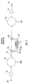
- FIG. 7 illustrates the use of a distributed Bragg grating region 81. The gratings can provide high reflectivity and wavelength selectivity.
- This tunable laser and filter apparatus can include a semiconductor substrate 82 and a laser structure 84 formed on the substrate.
- This laser structure includes an active layer 86, as known to those skilled in the art, and a plurality of Bragg grating structures 88 are formed along the active layer to form a Bragg grating and provide optical reflections at a desired Bragg wavelength.
- a microelectromechanical (MEMS) actuator 90 is operatively connected to each Bragg grating structure for changing the separation between Bragg grating structures and tuning the Bragg grating to a desired wavelength selectivity and limiting the laser output to a selected narrow-band mode.
- the apparatus can include an optical gain region 92 and also a phase adjust region 94 that are each selectively controlled via electrodes 96, 97.
- An electrode 98 also connects to the distributed Bragg grating 81. Electrodes 100 control the MEMS actuator.
- a surface emitting semiconductor laser of the type described can operate at high power levels and with high efficiency and can form a single far-field lobe in a single mode.
- the distributed feedback grating in the form of the Bragg grating is formed of periodically alternating grating elements to provide the optical feedback as a second order grating.
- Passive distributed Bragg reflection gratings can be formed adjacent the distributed feedback grating and provide near-field uniformity while maintaining high efficiency.
- the MEMS actuator for respective grating structures can be formed by standard photolithographic techniques as known to those skilled in the art.
- the distributed feedback laser applications are becoming more commonplace in the more advanced telecommunications systems and the use of dense wavelength division multiplexing (DWDM), allowing efficient combination of multi-channel (multi-carrier frequencies), and high-bit rate signals onto one optical fiber.
- the laser sources typically operate at 1310 nanometer and 1550 nanometer to transmit digital information at very high rates, even higher than 2.5 gigabits each second.
- the lasers emit light in the multi-longitudinal mode and the narrow band wavelengths cluster about a center wavelength. The interference between the different wavelengths limits the number of channels that can be transmitted along an optical fiber.
- the distributed feedback lasers use the grating within the laser medium as illustrated to act as a filter to limit the laser output to a single narrow-band mode required for long haul and high speed telecommunications.
- the tunable optical grating of the present invention has special applicability to tuning Bragg gratings and can be used in optical dispersion compensation and broadband optical beam forming for phased array antennas, as an example.
- Other uses of the tuned grating, in accordance with the present invention could include an optical amplifier gain spectrum flattening. It could also include adaptive optical equalization and reconfigurable optical add/drop multiplexing as illustrated in FIG. 1 and in other examples as known to those skilled in the art. It could be used with channel simulation and optical sensors, as well as tunable optical bandpass and band stop filters. It can also be used with active temperature compensation of DFB devices. These are all areas of technology known to those skilled in the art and the MEMS technology is especially applicable for these systems.
Abstract
Description
- This invention relates to optical diffraction and reflection gratings, and more particularly, this invention relates to Bragg gratings.
- Bragg gratings and similar fiber optic and other optical grating structures are produced in glass, plastic or silicon to spread out an optical spectrum or other radiation. These gratings usually consist of narrow, parallel slits or narrow, parallel, reflecting surfaces that break-up waves as they emerge.
- As is well known, light of all wavelengths is scattered at all angles. At some angles, however, light adds constructively at one wavelength, while other wavelengths add destructively (or interfere with each other), reducing the light intensity to zero or close to zero. In those ranges of angles where the grating spreads out a spectrum, there can be a gradual change in wavelength of the angle. With multiple grooves formed in a grating, light is concentrated in particular directions, and can be used as optical filters with other similar optical devices.
- One commonly used optical grating is a Bragg grating used as a periodic grating, a chirped grating, a distributed feedback or distributed Bragg reflector grating (DFF or DBR), such as with laser, and a Fabry-Perot Etalon grating for a ring resonator as designed for use with add/drop multiplexers and similar optical devices. A Bragg grating is the optical equivalent of a surface acoustic wave (SAW) device. By having a tuned grating, there can be some compensation for dispersion conditions. Some optical filters use Bragg gratings that are tuned during fabrication, temperature tuned, or compression/strained tuned. EP0486356 describes a Bragg grating tunable by piezoelectric means. EP0989437 and WO97/31289 describe fibre Bragg gratings tunable by applying a strain to the fibre. The document ZHANG X M et al, "A MEMS Pitch-tunable Grating Add/Drop Multiplexers", IEEE/LEOS INTERNATIONAL CONFERENCE ON OPTICAL MEMS, page 25-26, 21 August 2000, describes a thin grating tunable by MEMS actuators.
- Prior art solutions for tuning gratings using temperature or compression/strain methods have a limited tuning range of typically only tens of nanometers maximum with a slow operation of tuning. As is known, the temperature and strain changes on Bragg deflection and change are set forth as:
- The present invention is defined in the appended claims.
- Other objects, features and advantages of the present invention will become apparent from the detailed description of the invention which follows, when considered in light of the accompanying drawings in which:
- FIG. 1 is an example of a tunable optical grating of the present invention used in an add/drop multiplexer.
- FIG. 2 is an isometric view of a tunable optical grating of the present invention shown in the form of a Bragg grating.
- FIGS. 3, 4, 5 and 6 show multiple configurations possible with a single, tunable optical grating of the present invention, and showing a respective periodic, chirped, DFB, and Fabry-Perot Etalon grating.
- FIG. 7 is a schematic view of a tunable laser and filter apparatus of the present invention using a tunable Bragg grating.
- FIGS. 8, 9 and 10 are examples of different microelectromechanical (MEMS) actuators that can be used in the present invention.
-
- The present invention will now be described more fully hereinafter with reference to the accompanying drawings, in which preferred embodiments of the invention are shown. This invention may, however, be embodied in many different forms and should not be construed as limited to the embodiments set forth herein. Rather, these embodiments are provided so that this disclosure will be thorough and complete, and will fully convey the scope of the invention to those skilled in the art. Like numbers refer to like elements throughout.
- The present invention is advantageous and provides a tunable Bragg grating, using microelectromechanical (MEMS) actuators that are able to tune the grating over a much wider range, such as hundreds of nanometers. The present invention also allows multiple configurations within a single device.
- Referring now to FIGS. 1 and 2, there is illustrated in FIG. 1 at 20 an add/drop multiplexer that incorporates tunable Bragg
gratings 22a, 22b, such as shown in FIG. 2. As illustrated, the tunableoptical gratings 22a, 22b, in accordance with the invention, are placed in theoptical transmission path 24 as part of an overall optical transmission system that usesoptical circulators 26a, 26b.Amplifiers 28 can be placed at theinput side 30 oroutput side 32 of the grating that forms part of the add/drop multiplexer 20. The gratings are formed as Bragg reflective gratings and set to reflect wavelengths that are dropped within the first circulator 26a and wavelengths that are added within thesecond circulator 26b. Theamplifiers 28 can be used to adjust for any insertion losses in the add/drop and "through" pass. It is also possible to use different directional, optical couplers and optical isolators to provide selective add/drop capability, instead of use the described and illustrated optical circulators, as is known to those skilled in the art. Acentral processor 29, such as a processor as part of a personal computer, mini or mainframe, ASIC or other device known to those skilled in the art, controls the separator distance between grading structures (FIG. 2) by controlling individual MEMS actuators viacontrol lines 29a. - FIG. 2 illustrates an isometric view of a tunable
optical grating 30 of the present invention and having anoptical waveguide 34 in the form of a single fiber optic forming aninput port 35, which passes the optical signal, in the form of a wavelength division multiplexed signal through acollimating lens 36. The collimated signals then passes through a plurality ofgrating structures 38 formed as a Bragg grating (illustrated as a non-limiting example of four grating structures forming a Bragg grating) and into a converginglens 40. The optical signal passes through anoutput port 42 defined by another optical waveguide in the form of a single fiber optic. - In one aspect of the present invention, the
grating structures 38 are formed to be moveable on asilicon MEMS substrate 44 having formed MEMS actuators, and can be tuned such that the separation distance between the Bragg grating structures can be changed to tune the Bragg grating to a desired Bragg wavelength selectivity as shown by the ΛBRAGG. Thegrating structures 38 can be formed by semiconductor and photolithographic techniques known to those skilled in the art, and attached to MEMS actuators, such that the grating structures are moveable with MEMS actuator movement. - Referring now to FIGS. 3-6, there are illustrated four different types of gratings, which can be defined as a single device as shown in FIG. 2 where the separation distance between individual grating structures has been changed. FIG. 3 illustrates a simple periodic grating where the distance between grating structures is about the same. FIG. 4 illustrates a chirped grating where the gratings are progressively a greater distance from each other as light would pass from left to right. FIG. 5 illustrates a distributed feedback grating showing a separation between two groups of left and right gratings.
- FIG. 6 shows a Fabry-Perot Etalon showing a large gap between two sets of gratings as is common in a Fabry-Perot Etalong grating structure.
- FIGS. 8-10 illustrate various types of microelectromechanical (MEMS) actuators that can be used for changing the separation distance between the various Bragg
grating structures 38 in accordance with the present invention. Although the illustrated MEMS actuators show different types of movements for MEMS actuators, it should be understood that many different types of MEMS actuators can be used as suggested by those skilled in the art. The illustrated actuators are non-limiting examples for purposes of illustration. - FIG. 8 illustrates a flat, single
layer silicon member 50 that can be defined for an actuator structure. As is well known to those skilled in the art, silicon has a relatively high Young's modulus, e.g., about 139 to 190 GPa, allowing some actuator deflection capability. For example, for a 50 micrometer (UM) deflection, a 5 mm by 5 mm by 50 micrometer single layer silicon membrane can be used. Thesilicon membrane 50 is defined during its processing to have a bellows/lever MEMS structure 52. The bellows/lever structure can be manufactured by MEMS fabrication techniques known to those skilled in the art to form an actuator that moves the grating structures a predetermined distance based on inputs received from acontroller 29. The movement can even be on the order of a few nanometers. As a bellows moves, it could slide a lever or other interconnecting member and move the grating structure to which it is connected a predefined distance to form a grating, such as illustrated in FIGS. 3-6. - FIG. 9 illustrates in block format a hinged-
plate actuator 60 where alinkage 62 mechanically links and interconnects thehinged plate actuator 60 to agrating structure 38. Theactuator 60 imparts an inplane motion to thelinkage 62 to form a horizontal, back-and-forth reciprocating motion that moves thegrating structure 38 into a desired position. The actuator could be formed by two vertically oriented electrodes where one of the electrodes is moveable and the other electrode is fixed, as known to those skilled in the art. Voltage can be applied across the electrodes by a controlled voltage source and the moveable electrode would move or swing toward the fixed electrode. This horizontal displacement of the moveable electrode is transferred by linkage to the grating structure where it is then positioned into a desired location. - It is also possible to use a MEMS
deflectable beam member 70, as shown in FIG. 10, using a silicon, glass or quartz material, as known to those skilled in the art. The MEMS actuator can include ananchor 72 andbar member 74 slidably or otherwise operatively connected relative to the anchor and biased by an electrostatic charge that works in conjunction with aMEMS electrode 76, as known to those skilled in the art. - It is possible to form these and other MEMS actuators by techniques known to those skilled in the art, including standard photolithographic techniques. These techniques can include deep ion reactive etching of various channels and holes, and the deposition of various thermal oxide films, photolithography techniques, including photoresist application, and plasma etching.
- FIG. 7 illustrates a semiconducting tunable laser and
filter apparatus 80 where reflection occurs at a Bragg wavelength, as known to those skilled in the art. If a semiconducting polymer distributed feedback (DFB) laser is used, then the reflectors occur at the Bragg wavelength: λBRAGG = 2neff Λ, where neff is the effective refractive index. FIG. 7 illustrates the use of a distributed Bragg grating region 81. The gratings can provide high reflectivity and wavelength selectivity. This tunable laser and filter apparatus can include asemiconductor substrate 82 and alaser structure 84 formed on the substrate. This laser structure includes anactive layer 86, as known to those skilled in the art, and a plurality ofBragg grating structures 88 are formed along the active layer to form a Bragg grating and provide optical reflections at a desired Bragg wavelength. A microelectromechanical (MEMS)actuator 90 is operatively connected to each Bragg grating structure for changing the separation between Bragg grating structures and tuning the Bragg grating to a desired wavelength selectivity and limiting the laser output to a selected narrow-band mode. The apparatus can include anoptical gain region 92 and also a phase adjustregion 94 that are each selectively controlled viaelectrodes electrode 98 also connects to the distributed Bragg grating 81.Electrodes 100 control the MEMS actuator. - As is known to those skilled in the art, a surface emitting semiconductor laser of the type described can operate at high power levels and with high efficiency and can form a single far-field lobe in a single mode. The distributed feedback grating in the form of the Bragg grating is formed of periodically alternating grating elements to provide the optical feedback as a second order grating. Passive distributed Bragg reflection gratings can be formed adjacent the distributed feedback grating and provide near-field uniformity while maintaining high efficiency. The MEMS actuator for respective grating structures can be formed by standard photolithographic techniques as known to those skilled in the art.
- The distributed feedback laser applications are becoming more commonplace in the more advanced telecommunications systems and the use of dense wavelength division multiplexing (DWDM), allowing efficient combination of multi-channel (multi-carrier frequencies), and high-bit rate signals onto one optical fiber. The laser sources typically operate at 1310 nanometer and 1550 nanometer to transmit digital information at very high rates, even higher than 2.5 gigabits each second. The lasers emit light in the multi-longitudinal mode and the narrow band wavelengths cluster about a center wavelength. The interference between the different wavelengths limits the number of channels that can be transmitted along an optical fiber. The distributed feedback lasers use the grating within the laser medium as illustrated to act as a filter to limit the laser output to a single narrow-band mode required for long haul and high speed telecommunications.
- The tunable optical grating of the present invention has special applicability to tuning Bragg gratings and can be used in optical dispersion compensation and broadband optical beam forming for phased array antennas, as an example. Other uses of the tuned grating, in accordance with the present invention, could include an optical amplifier gain spectrum flattening. It could also include adaptive optical equalization and reconfigurable optical add/drop multiplexing as illustrated in FIG. 1 and in other examples as known to those skilled in the art. It could be used with channel simulation and optical sensors, as well as tunable optical bandpass and band stop filters. It can also be used with active temperature compensation of DFB devices. These are all areas of technology known to those skilled in the art and the MEMS technology is especially applicable for these systems.
- Many modifications and other embodiments of the invention will come to the mind of one skilled in the art having the benefit of the teachings presented in the foregoing descriptions and the associated drawings. Therefore, it is to be understood that the invention is not to be limited to the specific embodiments disclosed, and that the modifications and embodiments are intended to be included within the scope of the dependent claims.
Claims (11)
- A tunable optical Bragg grating comprising:a plurality of optical grating structures contained within an optical transmission path; characterised bya substantially planar microelectromechanical (MEMS) substrate on which the grating structures are formed and slidably moveable thereon and having a plurality of controllable microelectromechanical (MEMS) actuators operatively connected to said plurality of grating structures such that each actuator is operatively connected to a respective grating structure for physically moving the respective grating structure by sliding it relative to the MEMS substrate in a controlled manner and relative to an adjacent grating structure thereby changing the separation distance between grating structures and tuning the optical grating to a desired wavelength selectivity and permitting multiple configurations.
- A tunable optical grating according to Claim 1, wherein said grating structures form a periodic grating.
- A tunable optical grating according to Claim 1, wherein said grating structures form a chirped grating.
- A tunable optical grating according to Claim 1, wherein said grating structures form a distributed feedback grating.
- A tunable optical grating according to Claim 1, wherein said grating structures form Fabry-Perot Etalon add/drop grating structure.
- A tunable optical grating according to claim 1, wherein said MEMS actuator is photolithographically formed on said MEMS substrate.
- A tunable optical grating according to Claim 1, wherein said MEMS actuator comprises a flat, single layer silicon membrane structure.
- A tunable optical grating according to Claim 1, wherein said MEMS actuator comprises at least one anchor support and an arm member operatively connected to a grating structure and supported by the anchor support and movable therewith for physically moving said grating structure relative to another grating structure.
- A tunable optical grating according to Claim 1, wherein said MEMS actuator comprises a hinged plate actuator operatively connected to each grating structure.
- A tunable optical grating according to Claim 1, and further comprising an optical waveguide defining an input port through which an optical signal passes through said grating structures and an optical waveguide defining an output port for receiving the optical signal from the grating structures.
- A tunable optical grating structure according to Claim 10, and further comprising a collimating lens operatively connected to said input port and a converging lens operatively connected to said output port.
Applications Claiming Priority (3)
| Application Number | Priority Date | Filing Date | Title |
|---|---|---|---|
| US09/739,013 US6628851B1 (en) | 2000-12-20 | 2000-12-20 | MEMS reconfigurable optical grating |
| US739013 | 2000-12-20 | ||
| PCT/US2001/046980 WO2002059678A2 (en) | 2000-12-20 | 2001-12-06 | Mems reconfigurable optical grating |
Publications (2)
| Publication Number | Publication Date |
|---|---|
| EP1346241A2 EP1346241A2 (en) | 2003-09-24 |
| EP1346241B1 true EP1346241B1 (en) | 2005-06-22 |
Family
ID=24970449
Family Applications (1)
| Application Number | Title | Priority Date | Filing Date |
|---|---|---|---|
| EP01270125A Expired - Lifetime EP1346241B1 (en) | 2000-12-20 | 2001-12-06 | Mems reconfigurable optical grating |
Country Status (9)
| Country | Link |
|---|---|
| US (1) | US6628851B1 (en) |
| EP (1) | EP1346241B1 (en) |
| JP (1) | JP3899031B2 (en) |
| KR (1) | KR100493524B1 (en) |
| CN (1) | CN1275056C (en) |
| AT (1) | ATE298429T1 (en) |
| AU (1) | AU2002253803A1 (en) |
| DE (1) | DE60111649T2 (en) |
| WO (1) | WO2002059678A2 (en) |
Families Citing this family (21)
| Publication number | Priority date | Publication date | Assignee | Title |
|---|---|---|---|---|
| US20030016911A1 (en) * | 2001-07-19 | 2003-01-23 | Samad Talebpour | Random access optical add/drop switch |
| CA2377210A1 (en) * | 2001-07-25 | 2003-01-25 | Teraxion Inc. | Optical structure for the compensation of chromatic dispersion in a light signal |
| US6879755B2 (en) * | 2001-07-25 | 2005-04-12 | Teraxion Inc. | Optical structure for the compensation of chromatic dispersion and dispersion slope in a light signal |
| US20030179998A1 (en) * | 2002-03-22 | 2003-09-25 | Jianjun Zhang | Switchable bragg grating filter |
| US6973231B2 (en) * | 2001-10-22 | 2005-12-06 | International Optics Communications Corporation | Waveguide grating-based wavelength selective switch actuated by thermal mechanism |
| US6891989B2 (en) * | 2001-10-22 | 2005-05-10 | Integrated Optics Communications Corporation | Optical switch systems using waveguide grating-based wavelength selective switch modules |
| US20030123798A1 (en) * | 2001-12-10 | 2003-07-03 | Jianjun Zhang | Wavelength-selective optical switch with integrated Bragg gratings |
| KR100478508B1 (en) * | 2002-08-29 | 2005-03-28 | 한국전자통신연구원 | An Optical Add/Drop Apparatus |
| US20040228574A1 (en) * | 2003-05-14 | 2004-11-18 | Yu Chen | Switchable optical dispersion compensator using Bragg-grating |
| US20050018964A1 (en) * | 2003-07-24 | 2005-01-27 | Yu Chen | Compensation of Bragg wavelength shift in a grating assisted direct coupler |
| US7173764B2 (en) | 2004-04-22 | 2007-02-06 | Sandia Corporation | Apparatus comprising a tunable nanomechanical near-field grating and method for controlling far-field emission |
| US20050265720A1 (en) * | 2004-05-28 | 2005-12-01 | Peiching Ling | Wavelength division multiplexing add/drop system employing optical switches and interleavers |
| US8195118B2 (en) | 2008-07-15 | 2012-06-05 | Linear Signal, Inc. | Apparatus, system, and method for integrated phase shifting and amplitude control of phased array signals |
| US8699141B2 (en) | 2009-03-13 | 2014-04-15 | Knowles Electronics, Llc | Lens assembly apparatus and method |
| US8659835B2 (en) * | 2009-03-13 | 2014-02-25 | Optotune Ag | Lens systems and method |
| US20100290503A1 (en) * | 2009-05-13 | 2010-11-18 | Prime Photonics, Lc | Ultra-High Temperature Distributed Wireless Sensors |
| US8872719B2 (en) | 2009-11-09 | 2014-10-28 | Linear Signal, Inc. | Apparatus, system, and method for integrated modular phased array tile configuration |
| US8737846B2 (en) * | 2012-01-30 | 2014-05-27 | Oracle International Corporation | Dynamic-grid comb optical source |
| US9412480B2 (en) | 2013-05-09 | 2016-08-09 | Uchicago Argonne, Llc | Diffraction leveraged modulation of X-ray pulses using MEMS-based X-ray optics |
| CN104459677B (en) * | 2014-12-23 | 2017-02-22 | 苏州江奥光电科技有限公司 | Combined vernier grating and ranging system thereof |
| US10466423B2 (en) * | 2017-06-07 | 2019-11-05 | The Charles Stark Draper Laboratory, Inc. | Partitioned optical switch |
Family Cites Families (28)
| Publication number | Priority date | Publication date | Assignee | Title |
|---|---|---|---|---|
| FR2669120A1 (en) | 1990-11-13 | 1992-05-15 | Thomson Csf | A TWO-DIMENSIONAL LIGHT-DRIVEN PIEZOELECTRIC CONTROL LIGHT MODULATOR COMPRISING A BRAGG NETWORK. |
| JP2986604B2 (en) | 1992-01-13 | 1999-12-06 | キヤノン株式会社 | Semiconductor optical filter, method for controlling selected wavelength thereof, and optical communication system using the same |
| FR2716303B1 (en) * | 1994-02-11 | 1996-04-05 | Franck Delorme | Wavelength tunable distributed Bragg reflector laser with selectively activated virtual diffraction gratings. |
| US5502782A (en) * | 1995-01-09 | 1996-03-26 | Optelecom, Inc. | Focused acoustic wave fiber optic reflection modulator |
| US5781341A (en) | 1995-06-30 | 1998-07-14 | Dicon Fiberoptics, Inc. | Motorized tunable filter and motorized variable attenuator |
| US5757536A (en) | 1995-08-30 | 1998-05-26 | Sandia Corporation | Electrically-programmable diffraction grating |
| IL116536A0 (en) | 1995-12-24 | 1996-03-31 | Harunian Dan | Direct integration of sensing mechanisms with single crystal based micro-electric-mechanics systems |
| AU4778896A (en) | 1996-02-23 | 1997-09-10 | Electrophotonics Corporation | Apparatus and method for controlling the spectral response of a waveguide bragg grating |
| US5699468A (en) * | 1996-06-28 | 1997-12-16 | Jds Fitel Inc. | Bragg grating variable optical attenuator |
| US5706375A (en) * | 1996-09-10 | 1998-01-06 | Jds Fitel Inc. | Variable-attenuation tunable optical router |
| US5962949A (en) | 1996-12-16 | 1999-10-05 | Mcnc | Microelectromechanical positioning apparatus |
| US6124663A (en) | 1996-12-16 | 2000-09-26 | The Boeing Company | Fiber optic connector having a microelectromechanical positioning apparatus and an associated fabrication method |
| US6097859A (en) | 1998-02-12 | 2000-08-01 | The Regents Of The University Of California | Multi-wavelength cross-connect optical switch |
| US6069392A (en) | 1997-04-11 | 2000-05-30 | California Institute Of Technology | Microbellows actuator |
| US5999319A (en) | 1997-05-02 | 1999-12-07 | Interscience, Inc. | Reconfigurable compound diffraction grating |
| US5808384A (en) * | 1997-06-05 | 1998-09-15 | Wisconsin Alumni Research Foundation | Single coil bistable, bidirectional micromechanical actuator |
| US6035080A (en) | 1997-06-20 | 2000-03-07 | Henry; Charles Howard | Reconfigurable add-drop multiplexer for optical communications systems |
| US6122095A (en) | 1997-08-29 | 2000-09-19 | Lucent Technologies Inc. | Wavelength-selective and loss-less optical add/drop multiplexer |
| US6127908A (en) | 1997-11-17 | 2000-10-03 | Massachusetts Institute Of Technology | Microelectro-mechanical system actuator device and reconfigurable circuits utilizing same |
| US5974207A (en) | 1997-12-23 | 1999-10-26 | Lucent Technologies, Inc. | Article comprising a wavelength-selective add-drop multiplexer |
| US6011881A (en) | 1997-12-29 | 2000-01-04 | Ifos, Intelligent Fiber Optic Systems | Fiber-optic tunable filter |
| US5960131A (en) | 1998-02-04 | 1999-09-28 | Hewlett-Packard Company | Switching element having an expanding waveguide core |
| US6282340B1 (en) * | 1998-04-23 | 2001-08-28 | The Furukawa Electric Co., Ltd. | Light wavelength tuning device and light source optical demultiplexer and wavelength division multiplexed optical communication system using the tuning device |
| US6055348A (en) | 1998-09-23 | 2000-04-25 | Lucent Technologies Inc. | Tunable grating device and optical communication devices and systems comprising same |
| US6154471A (en) * | 1999-02-22 | 2000-11-28 | Lucent Technologies Inc. | Magnetically tunable and latchable broad-range semiconductor laser |
| US6363183B1 (en) * | 2000-01-04 | 2002-03-26 | Seungug Koh | Reconfigurable and scalable intergrated optic waveguide add/drop multiplexing element using micro-opto-electro-mechanical systems and methods of fabricating thereof |
| US6529659B2 (en) * | 2000-05-02 | 2003-03-04 | Parvenu, Inc. | Waveguide tunable Bragg grating using compliant microelectromechanical system (MEMS) technology |
| US6396855B1 (en) * | 2000-10-06 | 2002-05-28 | The Hong Kong Polytechnic University | Fibre gratings |
-
2000
- 2000-12-20 US US09/739,013 patent/US6628851B1/en not_active Expired - Lifetime
-
2001
- 2001-12-06 AT AT01270125T patent/ATE298429T1/en not_active IP Right Cessation
- 2001-12-06 CN CNB018221289A patent/CN1275056C/en not_active Expired - Fee Related
- 2001-12-06 DE DE60111649T patent/DE60111649T2/en not_active Expired - Lifetime
- 2001-12-06 EP EP01270125A patent/EP1346241B1/en not_active Expired - Lifetime
- 2001-12-06 KR KR10-2003-7008318A patent/KR100493524B1/en active IP Right Grant
- 2001-12-06 JP JP2002559742A patent/JP3899031B2/en not_active Expired - Fee Related
- 2001-12-06 WO PCT/US2001/046980 patent/WO2002059678A2/en active IP Right Grant
- 2001-12-06 AU AU2002253803A patent/AU2002253803A1/en not_active Abandoned
Also Published As
| Publication number | Publication date |
|---|---|
| WO2002059678A2 (en) | 2002-08-01 |
| CN1275056C (en) | 2006-09-13 |
| CN1620618A (en) | 2005-05-25 |
| WO2002059678A3 (en) | 2003-06-05 |
| JP2004525400A (en) | 2004-08-19 |
| DE60111649D1 (en) | 2005-07-28 |
| AU2002253803A1 (en) | 2002-08-06 |
| US6628851B1 (en) | 2003-09-30 |
| KR20030064850A (en) | 2003-08-02 |
| KR100493524B1 (en) | 2005-06-07 |
| EP1346241A2 (en) | 2003-09-24 |
| ATE298429T1 (en) | 2005-07-15 |
| DE60111649T2 (en) | 2006-05-18 |
| US20030194179A1 (en) | 2003-10-16 |
| JP3899031B2 (en) | 2007-03-28 |
Similar Documents
| Publication | Publication Date | Title |
|---|---|---|
| EP1346241B1 (en) | Mems reconfigurable optical grating | |
| US7634165B2 (en) | Monolithic tunable lasers and reflectors | |
| US10534137B2 (en) | Mirror based microelectromechanical systems and methods | |
| US7013064B2 (en) | Freespace tunable optoelectronic device and method | |
| US6791694B2 (en) | Tunable optical device using a scanning MEMS mirror | |
| US7483190B2 (en) | Method and apparatus for implementing a multi-channel tunable filter | |
| US8170384B1 (en) | Hybrid photonic signal processing modules | |
| JP2004522986A (en) | Tunable controlled laser array | |
| CA2454631A1 (en) | Method and apparatus for optical signal processing using an optical tapped delay line | |
| WO2002059653A2 (en) | Method and apparatus for implementing a multi-channel tunable filter | |
| US20030206681A1 (en) | Integrating element for optical fiber communication systems based on photonic multi-bandgap quasi-crystals having optimized transfer functions | |
| US20030223748A1 (en) | System and method for seamless spectral control | |
| US20200219818A1 (en) | Mirror based microelectromechanical systems and methods | |
| US20040096177A1 (en) | Variable optical attenuator with tunable wavelength selectivity | |
| US7289262B2 (en) | Optical attenuator element, and variable optical equalizer and optical amplifier that use this optical attenuator element | |
| US6571034B2 (en) | Spectrally-shaped optical components using a wavelength-dispersive element and a reflective array | |
| US7062120B2 (en) | Optical device and movable reflector | |
| Ford et al. | Interference-based micromechanical spectral equalizers | |
| US7068877B2 (en) | Movable mirror device, dispersion compensator, gain equalizer, and optical ADM apparatus | |
| CA2487612C (en) | Optical device and movable reflector | |
| WO2003093876A2 (en) | Integrating element for optical fiber communication systems based on photonic multi-bandgap quasi-crystals having optimized transfer functions | |
| WO2002037624A2 (en) | Wavelength-selective demultiplexer | |
| Okayama | Waveguide-Type Optical Wavelength Filters |
Legal Events
| Date | Code | Title | Description |
|---|---|---|---|
| PUAI | Public reference made under article 153(3) epc to a published international application that has entered the european phase |
Free format text: ORIGINAL CODE: 0009012 |
|
| 17P | Request for examination filed |
Effective date: 20030716 |
|
| AK | Designated contracting states |
Kind code of ref document: A2 Designated state(s): AT BE CH CY DE DK ES FI FR GB GR IE IT LI LU MC NL PT SE TR |
|
| AX | Request for extension of the european patent |
Extension state: AL LT LV MK RO SI |
|
| GRAP | Despatch of communication of intention to grant a patent |
Free format text: ORIGINAL CODE: EPIDOSNIGR1 |
|
| GRAS | Grant fee paid |
Free format text: ORIGINAL CODE: EPIDOSNIGR3 |
|
| GRAA | (expected) grant |
Free format text: ORIGINAL CODE: 0009210 |
|
| AK | Designated contracting states |
Kind code of ref document: B1 Designated state(s): AT BE CH CY DE DK ES FI FR GB GR IE IT LI LU MC NL PT SE TR |
|
| PG25 | Lapsed in a contracting state [announced via postgrant information from national office to epo] |
Ref country code: IT Free format text: LAPSE BECAUSE OF FAILURE TO SUBMIT A TRANSLATION OF THE DESCRIPTION OR TO PAY THE FEE WITHIN THE PRESCRIBED TIME-LIMIT;WARNING: LAPSES OF ITALIAN PATENTS WITH EFFECTIVE DATE BEFORE 2007 MAY HAVE OCCURRED AT ANY TIME BEFORE 2007. THE CORRECT EFFECTIVE DATE MAY BE DIFFERENT FROM THE ONE RECORDED. Effective date: 20050622 Ref country code: NL Free format text: LAPSE BECAUSE OF FAILURE TO SUBMIT A TRANSLATION OF THE DESCRIPTION OR TO PAY THE FEE WITHIN THE PRESCRIBED TIME-LIMIT Effective date: 20050622 Ref country code: TR Free format text: LAPSE BECAUSE OF FAILURE TO SUBMIT A TRANSLATION OF THE DESCRIPTION OR TO PAY THE FEE WITHIN THE PRESCRIBED TIME-LIMIT Effective date: 20050622 Ref country code: CH Free format text: LAPSE BECAUSE OF FAILURE TO SUBMIT A TRANSLATION OF THE DESCRIPTION OR TO PAY THE FEE WITHIN THE PRESCRIBED TIME-LIMIT Effective date: 20050622 Ref country code: FI Free format text: LAPSE BECAUSE OF FAILURE TO SUBMIT A TRANSLATION OF THE DESCRIPTION OR TO PAY THE FEE WITHIN THE PRESCRIBED TIME-LIMIT Effective date: 20050622 Ref country code: LI Free format text: LAPSE BECAUSE OF FAILURE TO SUBMIT A TRANSLATION OF THE DESCRIPTION OR TO PAY THE FEE WITHIN THE PRESCRIBED TIME-LIMIT Effective date: 20050622 Ref country code: BE Free format text: LAPSE BECAUSE OF FAILURE TO SUBMIT A TRANSLATION OF THE DESCRIPTION OR TO PAY THE FEE WITHIN THE PRESCRIBED TIME-LIMIT Effective date: 20050622 Ref country code: AT Free format text: LAPSE BECAUSE OF FAILURE TO SUBMIT A TRANSLATION OF THE DESCRIPTION OR TO PAY THE FEE WITHIN THE PRESCRIBED TIME-LIMIT Effective date: 20050622 |
|
| REG | Reference to a national code |
Ref country code: GB Ref legal event code: FG4D |
|
| REG | Reference to a national code |
Ref country code: CH Ref legal event code: EP |
|
| REG | Reference to a national code |
Ref country code: IE Ref legal event code: FG4D |
|
| REF | Corresponds to: |
Ref document number: 60111649 Country of ref document: DE Date of ref document: 20050728 Kind code of ref document: P |
|
| PG25 | Lapsed in a contracting state [announced via postgrant information from national office to epo] |
Ref country code: GR Free format text: LAPSE BECAUSE OF FAILURE TO SUBMIT A TRANSLATION OF THE DESCRIPTION OR TO PAY THE FEE WITHIN THE PRESCRIBED TIME-LIMIT Effective date: 20050922 Ref country code: DK Free format text: LAPSE BECAUSE OF FAILURE TO SUBMIT A TRANSLATION OF THE DESCRIPTION OR TO PAY THE FEE WITHIN THE PRESCRIBED TIME-LIMIT Effective date: 20050922 Ref country code: SE Free format text: LAPSE BECAUSE OF FAILURE TO SUBMIT A TRANSLATION OF THE DESCRIPTION OR TO PAY THE FEE WITHIN THE PRESCRIBED TIME-LIMIT Effective date: 20050922 |
|
| PG25 | Lapsed in a contracting state [announced via postgrant information from national office to epo] |
Ref country code: ES Free format text: LAPSE BECAUSE OF FAILURE TO SUBMIT A TRANSLATION OF THE DESCRIPTION OR TO PAY THE FEE WITHIN THE PRESCRIBED TIME-LIMIT Effective date: 20051003 |
|
| PG25 | Lapsed in a contracting state [announced via postgrant information from national office to epo] |
Ref country code: PT Free format text: LAPSE BECAUSE OF FAILURE TO SUBMIT A TRANSLATION OF THE DESCRIPTION OR TO PAY THE FEE WITHIN THE PRESCRIBED TIME-LIMIT Effective date: 20051129 |
|
| NLV1 | Nl: lapsed or annulled due to failure to fulfill the requirements of art. 29p and 29m of the patents act | ||
| PG25 | Lapsed in a contracting state [announced via postgrant information from national office to epo] |
Ref country code: CY Free format text: LAPSE BECAUSE OF FAILURE TO SUBMIT A TRANSLATION OF THE DESCRIPTION OR TO PAY THE FEE WITHIN THE PRESCRIBED TIME-LIMIT Effective date: 20051206 Ref country code: IE Free format text: LAPSE BECAUSE OF NON-PAYMENT OF DUE FEES Effective date: 20051206 |
|
| REG | Reference to a national code |
Ref country code: CH Ref legal event code: PL |
|
| PG25 | Lapsed in a contracting state [announced via postgrant information from national office to epo] |
Ref country code: MC Free format text: LAPSE BECAUSE OF NON-PAYMENT OF DUE FEES Effective date: 20051231 Ref country code: LU Free format text: LAPSE BECAUSE OF NON-PAYMENT OF DUE FEES Effective date: 20051231 |
|
| ET | Fr: translation filed | ||
| PLBE | No opposition filed within time limit |
Free format text: ORIGINAL CODE: 0009261 |
|
| STAA | Information on the status of an ep patent application or granted ep patent |
Free format text: STATUS: NO OPPOSITION FILED WITHIN TIME LIMIT |
|
| 26N | No opposition filed |
Effective date: 20060323 |
|
| REG | Reference to a national code |
Ref country code: IE Ref legal event code: MM4A |
|
| PGFP | Annual fee paid to national office [announced via postgrant information from national office to epo] |
Ref country code: GB Payment date: 20141229 Year of fee payment: 14 |
|
| REG | Reference to a national code |
Ref country code: FR Ref legal event code: PLFP Year of fee payment: 15 |
|
| GBPC | Gb: european patent ceased through non-payment of renewal fee |
Effective date: 20151206 |
|
| PG25 | Lapsed in a contracting state [announced via postgrant information from national office to epo] |
Ref country code: GB Free format text: LAPSE BECAUSE OF NON-PAYMENT OF DUE FEES Effective date: 20151206 |
|
| REG | Reference to a national code |
Ref country code: FR Ref legal event code: PLFP Year of fee payment: 16 |
|
| REG | Reference to a national code |
Ref country code: FR Ref legal event code: PLFP Year of fee payment: 17 |
|
| PGFP | Annual fee paid to national office [announced via postgrant information from national office to epo] |
Ref country code: FR Payment date: 20201227 Year of fee payment: 20 |
|
| PGFP | Annual fee paid to national office [announced via postgrant information from national office to epo] |
Ref country code: DE Payment date: 20201229 Year of fee payment: 20 |
|
| REG | Reference to a national code |
Ref country code: DE Ref legal event code: R071 Ref document number: 60111649 Country of ref document: DE |