EP1345325A2 - Solid-state relay - Google Patents
Solid-state relay Download PDFInfo
- Publication number
- EP1345325A2 EP1345325A2 EP03005627A EP03005627A EP1345325A2 EP 1345325 A2 EP1345325 A2 EP 1345325A2 EP 03005627 A EP03005627 A EP 03005627A EP 03005627 A EP03005627 A EP 03005627A EP 1345325 A2 EP1345325 A2 EP 1345325A2
- Authority
- EP
- European Patent Office
- Prior art keywords
- surge
- switching element
- voltage
- state
- current
- Prior art date
- Legal status (The legal status is an assumption and is not a legal conclusion. Google has not performed a legal analysis and makes no representation as to the accuracy of the status listed.)
- Granted
Links
Images


Classifications
-
- H—ELECTRICITY
- H03—ELECTRONIC CIRCUITRY
- H03K—PULSE TECHNIQUE
- H03K17/00—Electronic switching or gating, i.e. not by contact-making and –breaking
- H03K17/08—Modifications for protecting switching circuit against overcurrent or overvoltage
- H03K17/082—Modifications for protecting switching circuit against overcurrent or overvoltage by feedback from the output to the control circuit
- H03K17/0822—Modifications for protecting switching circuit against overcurrent or overvoltage by feedback from the output to the control circuit in field-effect transistor switches
-
- H—ELECTRICITY
- H03—ELECTRONIC CIRCUITRY
- H03K—PULSE TECHNIQUE
- H03K17/00—Electronic switching or gating, i.e. not by contact-making and –breaking
- H03K17/08—Modifications for protecting switching circuit against overcurrent or overvoltage
- H03K17/082—Modifications for protecting switching circuit against overcurrent or overvoltage by feedback from the output to the control circuit
- H03K17/0824—Modifications for protecting switching circuit against overcurrent or overvoltage by feedback from the output to the control circuit in thyristor switches
Definitions
- the present invention relates to a solid-state relay (SSR) for protecting a switching element from a lightning surge, and, more specifically, concerns a solid-state relay (SSR) which, in the event of a lightning surge during an off-state of the switching element, protects the switching element by forcefully turning the switching element on.
- SSR solid-state relay
- a surge absorbing element for example, a surge absorber
- a switching element parallel-connected to the load-connecting side of a switching element so that the surge voltage of a multiplexed lightning surge from the load side is limited to a value lower than the maximum rated voltage of the switching element so as to protect the switching element.
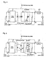
- Fig. 4 shows a block diagram that indicates one example of an essential portion of a conventional solid-state relay.
- a solid-state relay (SSR) 50 is provided with an input circuit 2, a photo-coupler 3, a resistor R1, a thyristor 4 and a surge absorber 5, and in this arrangement, a DC power supply VDC (or an AC power supply Vac) is applied between input terminals I1 and I2, and a load LD is connected to output terminals O1 and O2 with an AC power supply VAC being applied to the load LD.
- the load LD is constituted by a resistor, a lamp, a valve, an electromagnetic clutch, etc.
- the input circuit 2 is constituted by control circuits such as sequencers, and a control signal for controlling on-off states of the thyristor 4 serving as a switching element is supplied to a light-emitting diode of the photo-coupler 3 so as to allow an AC current to flow through the load LD or to stop it.
- the photo-coupler 3 is formed by a photo-thyristor that is bi-directionally connected to the light-emitting diode, and when a control signal (for example, a DC current) is supplied from the input circuit 2, the light-emitting diode emits light so that, upon receipt of the light, the photo-thyristor is turned on with an AC current flowing through the resistor R1 and a resistor R2 of the thyristor 4.
- a control signal for example, a DC current
- the thyristor 4 is formed by a triac that is a bi-directional AC switch; thus, when the voltage drop of the resistor R2 (gate voltage) has reached a predetermined value, the triac is turned on bi-directionally, and in contrast, when the voltage drop of the resistor R2 (gate voltage) goes below a holding voltage, the triac is turned off to form a switching element.
- the thyristor 4 When an AC current flows through the resistor R2 to cause a predetermined voltage drop, the thyristor 4 is turned on so that the output terminals 01 and O2 are short-circuited by a low impedance of the thyristor 4 to allow the AC current to flow through the load LD, thereby driving the load LD.
- the photo-coupler 3 When the control signal (for example, a DC current) from the input circuit 2 is stopped, the photo-coupler 3 is turned off so that the thyristor 4 is also turned off to open the output terminals O1 and O2; thus, the AC current is blocked and the driving operation of the load LD is stopped.
- a DC current for example, a DC current
- a bidirectional photo-thyristor is used as the photo-coupler 3 and a bi-directional triac is used as the thyristor 4 so that it is possible to switch an AC current having its polarity changed every half cycles.
- the application of the photo-coupler 3 insulates the DC current on the input circuit 2 side from the AC current on the thyristor 4 side so as to separate these from each other.
- the surge absorber 5 is parallel-connected to the thyristor 4, and placed on the output terminals O1 and O2 side; thus, in the case when a lightning surge that is induced by a transmission line and multiplexed on an AC power supply VAC is generated in the output terminals O1 and O2 through the load LD, this is determined by a surge resistant amount, and limited (surge-absorbed) to a surge voltage lower than the maximum rated voltage of the thyristor 4 so as to protect the thyristor 4 from the lightning surge.
- Fig. 5 shows a block diagram indicating an essential portion of another example of a conventional solid-state relay.
- a solid-state relay (SSR) 60 is provided with an input circuit 2, a PD (photodiode) array coupler 9, a resistor R3, an MOS-type FET (electric-field-effect transistor) 10 having n-channels and a surge absorber 5, and in this arrangement, a DC power supply VDC (or an AC power supply VAC) is applied between input terminals II and I2, and a load LD is connected to output terminals O1 and O2 with an AC power supply VAC being applied to the load LD.
- VDC or an AC power supply VAC
- the input circuit 2 is constituted by control circuits such as sequencers, and a control signal for controlling on-off states of the series-connected FET 10 (Q1 and Q2) serving as a switching element is supplied to a light-emitting diode of the PD (photodiode) array coupler 9 so as to allow an AC current to flow through the load LD or to stop it.
- control circuits such as sequencers, and a control signal for controlling on-off states of the series-connected FET 10 (Q1 and Q2) serving as a switching element is supplied to a light-emitting diode of the PD (photodiode) array coupler 9 so as to allow an AC current to flow through the load LD or to stop it.
- the PD (photodiode) array coupler 9 is constituted by n-number of photodiodes that are series-connected to the light-emitting diode, and when a control signal (for example, a DC current) is supplied from the input circuit 2, the light-emitting diode emits light, and upon receipt of the light, the n-number of photodiodes generate a predetermined voltage n ⁇ VD (VD represents a forward-direction voltage of the diode: approximately 0. 6 V) so that a current is allowed to flow the resistor R3 with a bias voltage VGS being applied between the gate G and source S of the FET 10 (Q1 and Q2).
- a control signal for example, a DC current
- VGS bias voltage supplied from the n-number of photodiodes of PD (photodiode) array coupler 9
- VGS bias voltage
- the n-number of photodiodes are used in the PD (photodiode) array coupler 9 and the FET 10 is used as the switching element so that it is possible to switch an AC current having its polarity changed every half cycles.
- the application of the PD (photodiode) array coupler 9 makes it possible to insulate the DC current on the input circuit 2 side from the AC current on the thyristor 4 side so as to separate these from each other.
- the surge absorber 5 is parallel-connected to the FET 10 and placed on the output terminals O1 and O2 side, and in the case when a lightning surge that is induced by a transmission line and multiplexed on an AC power supply VAC is generated in the output terminals O1 and O2 through the load LD, is determined by a surge resistant amount, and limited (surge-absorbed) to a surge voltage lower than the maximum rated voltage of the FET 10 so as to protect the FET 10 from the lightning surge.
- the FET (electric field effect transistor) 10 or the like is set to a value higher than the surge resistant amount (surge clamp voltage) of the surge absorber 5 with the lighting surge (surge voltage) to be multiplexed on the AC power supply VAC being set to a comparatively low level, it is possible to protect the switching element; however, in the case when the lightning surge (surge voltage) to be multiplexed is great, the surge absorber 5 fails to absorb this, with the result that the surge voltage to be applied to the switching element exceeds the maximum rated voltage of the switching element, and tends to damage the switching element.
- the damage to the switching element to be caused by the lightning surge can be prevented by adopting a surge absorber 5 having a greater surge resistant amount (having a low surge cramp voltage with a great absorbing capacity) or a switching element (thyristor 4, FET 10) having a greater maximum rated voltage; however, large-size surge absorber and switching element are required, consequently resulting in high costs.
- the present invention has been devised to solve the problems, and its objective is to provide a solid-state relay (SSR) which can positively protect a switching element from damages caused by lightning surge by using a simple structure.
- SSR solid-state relay
- a solid-state relay which has a switching element for controlling an on-state (conductive state) and an off-state (non-conductive state) of an electric current flowing through an external load based upon a control signal that is supplied from an input circuit, is provided with a surge protective means which, in the case when a multiplexed surge is applied from the load side during an off-state of the switching element, forcefully turns the switching element on based upon the lightning surge.
- the solid-state relay in accordance with the present invention which has a switching element for controlling an on-state (conductive state) and an off-state (non-conductive state) of an electric current flowing through an external load based upon a control signal that is supplied from an input circuit, is provided with a surge protective means which, in the case when a multiplexed lightning surge is applied from the load side during an off-state of the lightning switching element, forcefully turns the switching element on based upon the surge so that, in response to a lightning surge, it is possible to forcefully set the switching element in the on-state to lower the impedance of the switching element, and also to positively protect the switching element from lightning surge by using the surge protective means having a simple structure.
- the surge protective means in accordance with the present invention is provided with a surge-absorbing element.
- the surge protective means in accordance with the present invention is provided with a constant-voltage element.
- the surge protective means relating to the present invention is provided with a surge-absorbing element or a constant-voltage element, it is possible to apply a bias voltage to the switching element by operating the surge-absorbing element or the constant-voltage element to allow a current to flow in response to a multiplexed lightning surge, and consequently to forcefully turn the switching element on from the off-state to lower the impedance of the switching element.
- the surge protective means forcefully turns the switching element on by utilizing the lightning surge voltage to lower the impedance of the switching element, thereby making it possible to protect the switching element from the lightening surge.
- Fig. 1 shows a structural drawing that indicates one embodiment of a solid-state relay (SSR) in accordance with the present invention.
- a solid-state relay (SSR) 1 is provided with an input circuit 2, a photo-coupler 3, a resistor R1 a surge absorber 5, a switching element 6, a surge preventive means 7, input terminals I1, I2, and output terminals O1, O2, and an external DC power supply VDC (or an AC power supply Vac) is connected to the input terminals I1, I2, and an external load LD and AC power supply VAC are connected to the output terminals O1, O2.
- VDC or an AC power supply Vac
- the switching element 6 is formed by a thyristor 4 (for example, a triac) serving as a bi-directional switch, and when a current (for example, one portion of a surge current) caused by a lightning surge (surge voltage VSG) is allowed to flow through the resister R2 so that when the voltage drop of the resistor 2 has reached a predetermined gate voltage, it is set to the on-state, causing a reduction in the impedance (on-resistance) across the two ends of the thyristor 4, and short-circuiting the output terminals O1 and O2 to which the thyristor 4 is connected, by a low impedance.
- a thyristor 4 for example, a triac serving as a bi-directional switch
- the surge protective means 7 is constituted by a surge-absorbing element such as a surge absorber 8, and at the off-time of the switching element 6, a lightning surge (surge voltage VSA), multiplexed on an ac voltage VAC, is determined by the surge absorber 5 interpolated between the output terminals O1, O2 so that the limited surge voltage is applied between point A and point B through the register R1.
- a lightning surge surge voltage VSA
- VAC a lightning surge
- the surge protective means 7 allows a current (one portion of the surge current) to flow through a passage of the output terminal O1 ⁇ the resistor R1 ⁇ the surge protective means 7 (surge absorber 8) ⁇ the resistor R2 ⁇ the output terminal O2 (or a passage of the output terminal O2 ⁇ the resistor R2 ⁇ the surge protective means 7 (surge absorber 8) ⁇ the resistor R1 ⁇ the output terminal O1).
- the surge voltage VSG (VAC + VSG), multiplexed on the AC voltage VAC, which is applied between the output terminals O1 and O2, allows a greater current (AC current + surge current) to flow through the switching element 6 so that the surge voltage VSG is absorbed by the switching element 6, and reduced.
- the surge protective means 7 is operated by the surge voltage VSG (more specifically, AC voltage VAC + surge voltage VSG) to allow a current (one portion of surge current) to flow, and this state continues as long as the gate voltage of the thyristor 4 is maintained at a predetermined value (a voltage required for turning-on); however, since the continuous time of the surge voltage VSG is very short, no influences are actually caused even when the current flows through the load LG during the on-period of the switching element 6.
- VSG surge voltage
- VAC + surge voltage VSG AC voltage VAC + surge voltage VSG
- the solid-state relay (SSR) 1 is arranged so that, during the off-state of the switching element 6, the surge protective means 7 forcefully turns the switching element 6 on, based upon the surge voltage VSG multiplexed on the AC voltage VAC from the output terminals O1, O2; therefore, the surge current is allowed to flow by the low impedance (on-resistance) of the switching element 6 so that the surge voltage VSG is absorbed to be set to a low surge voltage VSG, thereby making it possible' to protect the switching element 6 from damages caused by the surge voltage VSG.
- the surge protective means 7 is provided with the surge-absorbing element (surge absorber 8), the surge-absorbing element (surge absorber 8) is operated to allow a current to flow upon receipt of a multiplexed lightning surge so that a bias voltage is applied to the switching element (thyristor 4); thus, the switching element (thyristor 4), which is in the off-state, is forcefully turned on so as to reduce the impedance of the switching element.
- Fig. 2 shows a structure of another embodiment of a solid-state relay (SSR) in accordance with the present invention.
- a solid-state relay (SSR) 11 is provided with an input circuit 2, a PD (photodiode) array coupler 9, a resistor R3, a surge absorber 5, a switching element 12, a surge preventive means 13, input terminals I1, I2, and output terminals O1, O2, and an external DC power supply VDC (or an AC power supply Vac) is connected to the input terminals I1, I2, and an external load LD and AC power supply VAC are connected to the output terminals O1, O2.
- a PD photodiode
- R3 resistor R3
- VDC or an AC power supply Vac
- the switching element 12 is formed by series-connecting MOS-type FETs Q1 and Q2 having n-channels, and in the case when, during the off-time (FETs Q1 and Q2 are off) of the switching element 12, a lightning surge (surge voltage VSG) is multiplexed on an AC power supply VAC from the output terminals O1, O2 (AC power supply VAC + surge voltage VSG), a current (one portion of a surge current) caused by the surge voltage VSG is allowed to flow through the surge protective means 13 so that a predetermined voltage n ⁇ VD (VD is a forward direction voltage of the diode: approximately 0.6 V) is generated in the n-number of photodiodes that are series-connected to the PD (photodiode) array coupler 9; thus, a current is allowed to flow through the resistor R3, while a bias voltage VGS is applied between gate G and source S of the FET Q1 and FET Q2 so that the FETs Q1 and Q2 are turned
- a constant-voltage element such as a Zener diode ZD1, and a resistor R4 are series-connected, and this is connected between point P1 and the upper anodes of the n-number of series-connected photodiodes of the PD (photodiode) array coupler 9, while a constant-voltage element, such as a Zener diode ZD2, and a resistor R5 are series-connected, and this is connected between point P2 and the upper anodes of the n-number of series-connected photodiodes of the PD (photodiode) array coupler 9.
- the combination of the Zener diode ZD1 and the resistor R4 is operated with respect to a surge voltage VSG that is multiplexed on the output terminal O1 side, while the combination of the Zener diode ZD2 and the resistor R5 is operated with respect to a surge voltage VSG that is multiplexed on the output terminal O2 side.
- the surge protective means 13 supplies a current (one portion of surge current) to the upper anodes of the n-number of series-connected photodiodes of the PD (photodiode) array coupler 9 through the resistor R4 or the resistor R5.
- a bias voltage VGS having a predetermined voltage n ⁇ VD (VD is a forward direction voltage of the diode: approximately 0.6 V) is generated in the n-number of photodiodes so that the bias voltage VGS is applied between the gate G and source S of the FET Q1 and FET Q2 of the switching element 12 so that the FET Q1 and FET Q2 are set to the on-state, thereby short-circuiting the output terminals O1 and O2 by a low impedance (on-resistance) of the FET Q1 and FET Q2.
- the surge voltage VSG (VAC + VSG)
- VAC + VSG the surge voltage VSG
- the on-state of the switching element 12 continues, as long as the surge protective means 13 is operated by the surge voltage VSG (more specifically, AC voltage VAC + surge voltage VSG) so that a current (one portion of surge current) is allowed to flow with the bias voltage VGS of the FET Q1 and FET Q2 being maintained at a predetermined value (a voltage required for turning-on); however, since the continuous time of the surge voltage VSG is very short, no influences are actually caused even when the current flows through the load LG during the on-period of the switching element 12.
- VSG surge voltage
- VAC + surge voltage VSG AC voltage VAC + surge voltage VSG
- the solid-state relay (SSR) 11 is arranged so that, during the off-state of the switching element 12, the surge protective means 13 forcefully turns the switching element 12 on, based upon the surge voltage VSG multiplexed on the AC voltage VAC from the output terminals O1, O2; therefore, the surge current is allowed to flow by the low impedance (on-resistance) of the switching element 12 so that the surge voltage VSG is absorbed to be set to a low surge voltage VSG, thereby making it possible to protect the switching element 12 from damages caused by the surge voltage VSG.
- the surge protective means 13 is provided with the constant-voltage elements ZD1, ZD2, the constant-voltage elements ZD1, ZD2 are operated to allow a current to flow upon receipt of a multiplexed lightning surge so that a bias voltage is applied to the switching element 12 (FET Q1 and FET Q2); thus, the switching element 12, which is in the off-state, is forcefully turned on so as to reduce the impedance of the switching element 12.
- Fig. 3 shows an applied waveform diagram of a surge voltage (VSG) of a lightning surge.
- Fig. 3A shows a waveform diagram that indicates a case in which, without the surge absorber 5, the surge protective means 7 (see Fig. 1) and the surge protective means 13 (see Fig. 2), a surge voltage VSG of 10 kV is applied from a lightning surge tester.
- Fig. 3B shows a case in which, when the surge absorber 5 is inserted as shown in Fig. 1 or Fig. 2, the surge voltage VSG (10 kV) of Fig. 3A is absorbed by the surge absorber 5 so that the surge-absorbing effect for forming a reduced surge voltage VSG1 is exerted.
- Fig. 3C shows a case in which, when the surge protective means 7 is inserted as shown in Fig. 1 or when the surge protective means 13 is inserted as shown in Fig. 2, in addition to the surge absorber 5 of Fig. 3B, the surge voltage VSG (10 kV) of Fig. 3A is absorbed by the surge absorber 5 and the surge protective means 7 (or the surge protective means 13) so that the surge absorbing effect for forming a reduced surge voltage VSG2 is exerted.
- the solid-state relay in accordance with the present invention which has a switching element for controlling an on-state (conductive state) and an off-state (non-conductive state) of an electric current flowing through an external load based upon a control signal that is supplied from an input circuit, is provided with a surge protective means which, in the case when a multiplexed lightning surge is applied from the load side during an off-state of the switching element, forcefully turns the switching element on based upon the lightning surge so that, in response to a lightning surge, it is possible to forcefully set the switching element in the on-state to lower the impedance of the switching element, and also to positively protect the switching element from lightning surge by using the surge protective means having a simple structure.
- the surge protective means relating to the present invention is provided with a surge-absorbing element or a constant-voltage element, it is possible to apply a bias voltage to the switching element by operating the surge-absorbing element or the constant-voltage element to allow a current to flow in response to a multiplexed lightning surge, and consequently to forcefully turn the switching element on from the off-state to lower the impedance of the switching element.
Landscapes
- Electronic Switches (AREA)
- Emergency Protection Circuit Devices (AREA)
- Control Of Electrical Variables (AREA)
- Power Conversion In General (AREA)
Abstract
Description
Claims (3)
- A solid-state relay, which has a switching element for controlling an on-state (conductive state) and an off-state (non-conductive state) of an electric current flowing through an external load based upon a control signal that is supplied from an input circuit, comprising:surge protective means which, in the case when a multiplexed surge is applied from said load side during an off-state of said switching element, forcefully turns said switching element on based upon the surge.
- The solid-state relay according to claim 1, wherein said surge protective means comprises a surge absorbing element.
- The solid-state relay according to claim 1, wherein said surge protective means comprises a constant-voltage element.
Applications Claiming Priority (2)
| Application Number | Priority Date | Filing Date | Title |
|---|---|---|---|
| JP2002072728 | 2002-03-15 | ||
| JP2002072728A JP2003274636A (en) | 2002-03-15 | 2002-03-15 | Solid state relay |
Publications (3)
| Publication Number | Publication Date |
|---|---|
| EP1345325A2 true EP1345325A2 (en) | 2003-09-17 |
| EP1345325A3 EP1345325A3 (en) | 2005-09-14 |
| EP1345325B1 EP1345325B1 (en) | 2008-09-10 |
Family
ID=27764570
Family Applications (1)
| Application Number | Title | Priority Date | Filing Date |
|---|---|---|---|
| EP03005627A Expired - Lifetime EP1345325B1 (en) | 2002-03-15 | 2003-03-12 | Solid-state relay |
Country Status (5)
| Country | Link |
|---|---|
| US (1) | US7023681B2 (en) |
| EP (1) | EP1345325B1 (en) |
| JP (1) | JP2003274636A (en) |
| CN (2) | CN2704158Y (en) |
| DE (1) | DE60323419D1 (en) |
Cited By (1)
| Publication number | Priority date | Publication date | Assignee | Title |
|---|---|---|---|---|
| FR2986926A1 (en) * | 2012-02-15 | 2013-08-16 | Airbus Operations Sas | Switching module for opening or closing connection between node of power supply circuit and connection node of load circuit, has controlled switch preventing current flow in switching module in direction opposed to operation direction |
Families Citing this family (14)
| Publication number | Priority date | Publication date | Assignee | Title |
|---|---|---|---|---|
| JP2005302925A (en) * | 2004-04-09 | 2005-10-27 | Toshiba Corp | Semiconductor device |
| JP2006186344A (en) * | 2004-12-02 | 2006-07-13 | Toshiba Corp | Optical coupling device |
| US7254003B2 (en) * | 2005-03-24 | 2007-08-07 | Freescale Semiconductor, Inc. | Differential nulling avalanche (DNA) clamp circuit and method of use |
| US7746155B2 (en) * | 2005-03-30 | 2010-06-29 | Texas Instruments Incorporated | Circuit and method for transistor turn-off with strong pulldown |
| US20060291114A1 (en) * | 2005-06-27 | 2006-12-28 | Teo Chee K | Electrostatic discharge protection circuit and method |
| US7737762B2 (en) * | 2006-09-12 | 2010-06-15 | Energate Inc | Solid-state switch |
| CN101588057B (en) * | 2008-05-22 | 2011-05-18 | 上海继电器有限公司 | Relay protection device |
| JP5407349B2 (en) * | 2009-01-15 | 2014-02-05 | ダイキン工業株式会社 | Switch circuit |
| GB2486493B (en) * | 2010-12-17 | 2016-06-15 | Ge Aviat Systems Ltd | Switching circuits and methods of testing |
| WO2016194436A1 (en) * | 2015-06-05 | 2016-12-08 | シャープ株式会社 | Solid state relay, power triac chip, and method for testing solid state relay |
| US10411694B2 (en) | 2016-07-22 | 2019-09-10 | Abb Schweiz Ag | Solid state switch system |
| US10554201B2 (en) | 2016-07-22 | 2020-02-04 | Abb Schweiz Ag | Solid state switch system |
| CN109672144B (en) * | 2018-11-29 | 2020-01-31 | 杭州电子科技大学 | single-phase AC solid-state relay circuit with earth leakage protection |
| US12415601B2 (en) * | 2022-11-29 | 2025-09-16 | Textron Innovations Inc. | Electrically isolated auxiliary flight controllers for rotorcraft |
Family Cites Families (6)
| Publication number | Priority date | Publication date | Assignee | Title |
|---|---|---|---|---|
| JPH0247132B2 (en) | 1981-03-25 | 1990-10-18 | Fuji Electric Co Ltd | GYAKUHEIRETSUSAIRISUTATENKOSOCHI |
| JPS5839264A (en) | 1981-09-01 | 1983-03-07 | Fuji Electric Co Ltd | Protecting system for overvoltage of photo-thyristor |
| US4395637A (en) * | 1981-12-07 | 1983-07-26 | Bell Telephone Laboratories, Incorporated | Optically toggled latch-free normally off switch |
| DE3311667C2 (en) | 1983-03-30 | 1986-02-13 | Siemens AG, 1000 Berlin und 8000 München | Arrangement for the feedback of protective ignitions with two series-connected counter-parallel thyristor pairs |
| US4970623A (en) * | 1988-12-29 | 1990-11-13 | Hewlett-Packard Company | Peripheral device power activation circuit and method therefor |
| FI107662B (en) | 1997-06-10 | 2001-09-14 | Lexel Finland Ab Oy | Transient |
-
2002
- 2002-03-15 JP JP2002072728A patent/JP2003274636A/en active Pending
-
2003
- 2003-03-05 CN CNU032015992U patent/CN2704158Y/en not_active Expired - Fee Related
- 2003-03-05 CN CN03107090.6A patent/CN1212706C/en not_active Expired - Fee Related
- 2003-03-10 US US10/383,878 patent/US7023681B2/en not_active Expired - Lifetime
- 2003-03-12 DE DE60323419T patent/DE60323419D1/en not_active Expired - Lifetime
- 2003-03-12 EP EP03005627A patent/EP1345325B1/en not_active Expired - Lifetime
Cited By (1)
| Publication number | Priority date | Publication date | Assignee | Title |
|---|---|---|---|---|
| FR2986926A1 (en) * | 2012-02-15 | 2013-08-16 | Airbus Operations Sas | Switching module for opening or closing connection between node of power supply circuit and connection node of load circuit, has controlled switch preventing current flow in switching module in direction opposed to operation direction |
Also Published As
| Publication number | Publication date |
|---|---|
| CN1445929A (en) | 2003-10-01 |
| CN2704158Y (en) | 2005-06-08 |
| JP2003274636A (en) | 2003-09-26 |
| US20030231444A1 (en) | 2003-12-18 |
| EP1345325A3 (en) | 2005-09-14 |
| US7023681B2 (en) | 2006-04-04 |
| CN1212706C (en) | 2005-07-27 |
| EP1345325B1 (en) | 2008-09-10 |
| DE60323419D1 (en) | 2008-10-23 |
Similar Documents
| Publication | Publication Date | Title |
|---|---|---|
| EP1345325B1 (en) | Solid-state relay | |
| US7948719B2 (en) | Solid state circuit protection system that works with arc fault circuit interrupter | |
| US20100208401A1 (en) | Inductive load driving circuit | |
| EP2472707B1 (en) | Semiconductor drive device | |
| US10186857B2 (en) | Paralleling mechanical relays for increased current carrying and switching capacity | |
| US20170272158A1 (en) | Driver system with an optical power based isolated power supply | |
| EP3164927B1 (en) | Apparatus to provide reverse polarity protection | |
| US6256185B1 (en) | Low voltage direct control universal pulse width modulation module | |
| KR101206215B1 (en) | Electronic magnetic contactor | |
| EP0219925B1 (en) | Switching device | |
| US7031129B2 (en) | Protection circuit | |
| JP3870808B2 (en) | Method and circuit for protecting switching element for solenoid drive | |
| SE0302587D0 (en) | Circuit device for high speed switching of inductive loads | |
| JP6724539B2 (en) | Load drive | |
| RU2343580C1 (en) | Electromagnetic drive | |
| US20030025546A1 (en) | Protection circuit | |
| EP0220791B1 (en) | Switching device | |
| US20160272133A1 (en) | Current regulator for an inductive load in a vehicle | |
| US6421260B1 (en) | Shutdown circuit for a half-bridge converter | |
| KR100313376B1 (en) | Electric Shock Protecting Circuit | |
| KR100933743B1 (en) | Relay contact overheat protection circuit | |
| JP4044771B2 (en) | Drive device for piezoelectric actuator | |
| JP5091312B2 (en) | Apparatus and method for identifying a control scheme for a switchgear that releases voltage or current | |
| KR100387486B1 (en) | Short protection circuit | |
| JP2025011032A (en) | Driver for driving an electromechanical device |
Legal Events
| Date | Code | Title | Description |
|---|---|---|---|
| PUAI | Public reference made under article 153(3) epc to a published international application that has entered the european phase |
Free format text: ORIGINAL CODE: 0009012 |
|
| AK | Designated contracting states |
Kind code of ref document: A2 Designated state(s): AT BE BG CH CY CZ DE DK EE ES FI FR GB GR HU IE IT LI LU MC NL PT SE SI SK TR |
|
| AX | Request for extension of the european patent |
Extension state: AL LT LV MK RO |
|
| PUAL | Search report despatched |
Free format text: ORIGINAL CODE: 0009013 |
|
| AK | Designated contracting states |
Kind code of ref document: A3 Designated state(s): AT BE BG CH CY CZ DE DK EE ES FI FR GB GR HU IE IT LI LU MC NL PT SE SI SK TR |
|
| AX | Request for extension of the european patent |
Extension state: AL LT LV MK RO |
|
| 17P | Request for examination filed |
Effective date: 20060314 |
|
| AKX | Designation fees paid |
Designated state(s): DE FR IT |
|
| 17Q | First examination report despatched |
Effective date: 20070725 |
|
| GRAP | Despatch of communication of intention to grant a patent |
Free format text: ORIGINAL CODE: EPIDOSNIGR1 |
|
| GRAS | Grant fee paid |
Free format text: ORIGINAL CODE: EPIDOSNIGR3 |
|
| GRAA | (expected) grant |
Free format text: ORIGINAL CODE: 0009210 |
|
| AK | Designated contracting states |
Kind code of ref document: B1 Designated state(s): DE FR IT |
|
| REF | Corresponds to: |
Ref document number: 60323419 Country of ref document: DE Date of ref document: 20081023 Kind code of ref document: P |
|
| PLBE | No opposition filed within time limit |
Free format text: ORIGINAL CODE: 0009261 |
|
| STAA | Information on the status of an ep patent application or granted ep patent |
Free format text: STATUS: NO OPPOSITION FILED WITHIN TIME LIMIT |
|
| 26N | No opposition filed |
Effective date: 20090611 |
|
| REG | Reference to a national code |
Ref country code: DE Ref legal event code: R082 Ref document number: 60323419 Country of ref document: DE Representative=s name: KILIAN KILIAN & PARTNER, DE Ref country code: DE Ref legal event code: R082 Ref document number: 60323419 Country of ref document: DE Representative=s name: KILIAN KILIAN & PARTNER MBB PATENTANWAELTE, DE |
|
| REG | Reference to a national code |
Ref country code: FR Ref legal event code: PLFP Year of fee payment: 14 |
|
| REG | Reference to a national code |
Ref country code: FR Ref legal event code: PLFP Year of fee payment: 15 |
|
| REG | Reference to a national code |
Ref country code: FR Ref legal event code: PLFP Year of fee payment: 16 |
|
| PGFP | Annual fee paid to national office [announced via postgrant information from national office to epo] |
Ref country code: IT Payment date: 20190222 Year of fee payment: 10 |
|
| PGFP | Annual fee paid to national office [announced via postgrant information from national office to epo] |
Ref country code: DE Payment date: 20200225 Year of fee payment: 18 |
|
| PGFP | Annual fee paid to national office [announced via postgrant information from national office to epo] |
Ref country code: FR Payment date: 20200214 Year of fee payment: 18 |
|
| REG | Reference to a national code |
Ref country code: DE Ref legal event code: R119 Ref document number: 60323419 Country of ref document: DE |
|
| PG25 | Lapsed in a contracting state [announced via postgrant information from national office to epo] |
Ref country code: IT Free format text: LAPSE BECAUSE OF NON-PAYMENT OF DUE FEES Effective date: 20200312 |
|
| PG25 | Lapsed in a contracting state [announced via postgrant information from national office to epo] |
Ref country code: FR Free format text: LAPSE BECAUSE OF NON-PAYMENT OF DUE FEES Effective date: 20210331 Ref country code: DE Free format text: LAPSE BECAUSE OF NON-PAYMENT OF DUE FEES Effective date: 20211001 |