EP1345319A2 - Method and system for reducing non-linearities - Google Patents
Method and system for reducing non-linearities Download PDFInfo
- Publication number
- EP1345319A2 EP1345319A2 EP02023149A EP02023149A EP1345319A2 EP 1345319 A2 EP1345319 A2 EP 1345319A2 EP 02023149 A EP02023149 A EP 02023149A EP 02023149 A EP02023149 A EP 02023149A EP 1345319 A2 EP1345319 A2 EP 1345319A2
- Authority
- EP
- European Patent Office
- Prior art keywords
- signal
- circuit
- input
- generation circuit
- envelope
- Prior art date
- Legal status (The legal status is an assumption and is not a legal conclusion. Google has not performed a legal analysis and makes no representation as to the accuracy of the status listed.)
- Withdrawn
Links
Images

Classifications
-
- H—ELECTRICITY
- H03—ELECTRONIC CIRCUITRY
- H03F—AMPLIFIERS
- H03F1/00—Details of amplifiers with only discharge tubes, only semiconductor devices or only unspecified devices as amplifying elements
- H03F1/32—Modifications of amplifiers to reduce non-linear distortion
- H03F1/3241—Modifications of amplifiers to reduce non-linear distortion using predistortion circuits
- H03F1/3247—Modifications of amplifiers to reduce non-linear distortion using predistortion circuits using feedback acting on predistortion circuits
Definitions
- the present invention relates in general to the field of signal generation, and in particular, by way of example but not limitation, to reduction of non-linearities in signal-generation circuits.
- a major objective of the present invention is to reduce non-linearities in signal-generation circuits.
- Attempts to improve the linearity of a series combination of a modulator and power amplifier include: (a) choosing components that are more linear; and (b) using linearization techniques such as, for example, feedback, feedforward, and pre-distortion.
- Feedback generally refers to feeding back at least a part of a signal to a delayed version of the signal in order to correct the signal substantially in real time.
- Feedforward generally refers to correcting a signal in advance so the future signals are corrected. Because components that exhibit greater linearity are often more expensive than components that exhibit lesser linearity, linearization techniques that correct non-linearities of the less-linear components have been pursued.
- Feedback linearization generally has two forms: 1) polar; and 2) Cartesian. Linearization can be applied to either a base-band signal, an IF (intermediate-frequency) signal (if one exists), or a radio-frequency (RF) signal. In general, feedback loop delays tend to limit the available signal bandwidth and can lead to instability if bandwidth restrictions are exceeded.
- Feedforward linearization operates by measuring distortion from non-linearities, delaying a main signal, and subtracting the distortion from the main signal using the measured distortion. Feedforward linearization tends to be used for reducing effects of non-linearities in RF components, such as, for example, a PA. Modulator errors are not typically corrected using feedforward linearization. Feedforward linearization performance is typically limited by the quality of a second, reference amplifier, used to amplify the measured distortion. Disadvantages of using feedforward compensation include expense and the need for precise balances between reference and signal paths in order to obtain acceptable performance.
- Pre-distortion linearization involves the introduction of non-linearities into a signal path.
- the non-linearities are then used to counteract non-linearities present in the original components, such as, for example, the modulator and the PA.
- An objective of pre-distortion is to keep constant the gain of the series combination of a pre-distorter (PD), the modulator, and the PA, despite instantaneous signal power-level variations due to time-varying (e.g., amplitude-modulation (AM)) components of the signal.
- Pre-distortion linearization can be applied anywhere along the signal path; however, in certain applications, pre-distortion linearization of the base-band or of the RF signal might be preferred.
- Pre-distortion linearization typically compensates for the modulator and PA non-linearities by modeling as a parametric function a time-varying inverse of the non-linear gain of the system. Pre-distortion parameters that minimize the output distortion are also usually estimated. When the pre-distortion is perfect, the parameters of the inverse non-linear gain are identical to those minimizing the output distortion. Adaptive estimation of the pre-distortion parameters is desirable because the gain can drift over time.
- the adaptive parameter estimation typically requires that the gain variations be measured accurately. Inaccurate measurements of the gain variations can bias the parameter estimation, thereby impairing the performance of pre-distortion linearization.
- the present invention provides a method and system for improving the linearity of circuits such as signal-generation circuits using a measurement circuit that is not required to be ultra-linear and is therefore less expensive than other approaches.
- a time-varying signal with an AM component is input to a circuit in order to excite non-linearities of the circuit.
- the measurement circuit is balanced to remove the AM component so that the resulting signal does not excite any non-linearities of the measurement circuit. Any such non-linearities of the measurement circuit are minimized by extracting a portion of the signal that passes through the circuit. The extracted portion does not have a substantial time-varying component.
- non-linearities of the measurement circuit are not excited, while non-linearities of the circuit are excited and can therefore be measured and subsequently corrected.
- a method of reducing non-linearities of a circuit includes providing and pre-distorting an input signal.
- the input signal includes a constant component and a time-varying component.
- the pre-distorted input signal is input to the circuit and an output signal is obtained from the circuit.
- a carrier signal is subtracted from the output signal, thereby yielding an error signal.
- An error signal envelope is determined and is demodulated using a demodulating signal related to the input signal.
- the parameters of the pre-distorted input signal are adjusted with reference to the demodulated converted error signal, thereby causing an amplitude of the error signal envelope to approach a constant value.
- a system for reducing non-linearities includes an input-signal-generation circuit and a carrier-signal-generation circuit.
- the signal-generation circuit is adapted to generate an input signal having a constant component and a time-varying component.
- the carrier-signal-generation circuit is adapted to generate a carrier signal.
- the circuit includes an input connected to the input-signal-generation circuit and adapted to receive the input signal and a modulator connected to the carrier-signal-generation circuit and adapted to modulate the input signal with the carrier signal.
- the circuit also includes an amplifier, connected to the modulator, adapted to amplify the modulated input signal. An output is connected to the amplifier and is adapted to output the modulated amplified input signal.
- the system includes a pre-distorter that is adapted to adjust signal parameters.
- the pre-distorter is connected to the circuit.
- the measurement circuit is adapted to yield an envelope of an error signal.
- the envelope comprises a function of an imbalance of the measurement circuit. Pre-distortion parameter adjustments are used to cause an amplitude of an envelope of the error signal to approach a constant value, thereby reducing non-linearities of the circuit.
- FIG. 1 is a block diagram of a linearization circuit 100 in accordance with teachings of the present invention.
- the linearization circuit 100 which has a base-band input signal x(t), could be, for example, an Agilent ESG-D Falcon signal generator.
- the base-band input signal x(t) comprises a quadrature pair of base-band signals, denoted by I and Q (i.e., in-phase and quadrature components), respectively.
- An output of the linearization circuit 100 is an RF signal denoted by RF ( t ).
- a modulator 102 and a power amplifier (PA) 104 are arranged in series.
- a local oscillator (LO) 106 provides an RF input signal to the modulator 102.
- LO local oscillator
- pre-distortion can be applied anywhere along the signal path. Even though pre-distortion can be applied anywhere along the signal path, such as, for example, prior to the modulator 102, on the RF signal path between the modulator 102 and the PA 104, or after the PA 104, pre-distortion of the base-band input x(t) is often preferred because of ease of implementation.
- a pre-distorter (PD) 108 distorts x(t) and then provides a pre-distorted signal to a digital-to-analog converter (DAC) 110, which outputs to the modulator 102.
- Pre-distortion settings 112 can be made to the PD 108 via a controller 114. The pre-distortion settings 112 allow adjustments to be made to parameters of the PD 108 in order to improve linearity of the linearization circuit 100.
- the output signal is fed to an output device, such as, for example, an antenna, and also to the gain-adjustment block 118.
- the output of the gain-adjustment block 118 is fed to a combiner 122, which also receives the inverse of the output of the LO 106, after phase adjustment by the phase-adjustment block 120, as an input.
- the gain-adjustment block 118 and the phase-adjustment block 120 are used to align the gain and phase of the output signal and of the output of the modulator 102 so that each of the signals is of similar phase and average power.
- the pre-distortion settings 112 of the PD 108 are adjusted manually.
- the pre-distortion settings 112 are typically adjusted via a one-time procedure.
- Higher complexity pre-distortion involves automatic adjustment of the pre-distortion settings 112.
- Automatic adjustment of the pre-distortion settings 112 can be grouped into two general classes: 1) off-line calibration; and 2) on-line adaptation.
- Off-line calibration uses known input signals to determine adjustments to the pre-distortion settings 112. In off-line calibration, use of the linearization circuit 100 is suspended. In contrast, in on-line adaptation, the settings 112 are adjusted while the linearization circuit 100 is in use and the input signal x(t) is being used.
- linearity of devices that use modulators and amplifiers to convert base-band signals to RF can be improved.
- embodiments of the present invention eliminate offsets between desired gain and actual gain.
- the PD 108 can be made to introduce a non-linearity into the signal path of the linearization circuit 100 in order to compensate for subsequently-introduced non-linearities by, for example, the modulator 102 and the PA 104.
- the PD 108 is adjusted by inputting the signal x(t) (after pre-distortion) to the modulator 102 and measuring an error signal. As the pre-distortion reduces the gain offsets and improves the linearity of the linearization circuit 100, the error signal converges towards a constant value.
- Selection of an appropriate input signal x(t) helps to ensure that non-linear modes within the modulator 102 and the PA 104 are stimulated and also enables extraction of a portion of the output signal that does not stimulate non-linear modes of any of the blocks 118 or 120 or of the combiner 122 or diode 124. As a result, accurate, bias-free parameter estimates can be obtained using inexpensive, relatively non-linear, components.
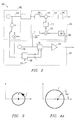
- FIG. 2 is a detailed block diagram of a linearization circuit 200 in accordance with teachings of the present invention.
- the linearization circuit 200 includes a signal-generation circuit 201, an input-signal-generation circuit 202, and a measurement circuit 203.
- the signal s mod ( t ) performs two principal functions: (1) s mod ( t ) stimulates non-linear modes of the modulator 102 and the PA 104 by varying an amplitude of the input signal x i (t); and 2) s mod (t) disrupts an instantaneous balance of the measurement circuit 203, which can also be referred to as am measurement bridge circuit, so that optimal settings of the PD 108 can be determined.
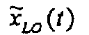
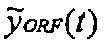
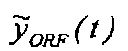
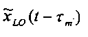
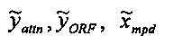
- Other signals shown in FIG. 4 are (i.e., the modulating, or LO, signal), (i.e., a pre-distorted and modulated input signal), and (i.e., an RF error signal), wherein: and respectively, and x LO (t), x mpd (t), and ⁇ RF (t) are the respective complex baseband signals.
- the LO signal output by the LO 106 is input to the modulator 102, which up-converts a pre-distorted input signal to RF, thereby yielding the modulated pre-distorted input signal .
- a phase-shifted version of the LO signal is subtracted from a gain-adjusted sample of the output signal , thereby yielding the error signal .
- the error signal is output by a combiner 210 of the measurement circuit 203.
- the measurement circuit 203 includes two paths, a reference path 206 and an output path 208, which are nominally balanced in terms of amplitude and are 180 degrees offset in phase from one another.
- the reference path 206 carries a replica of the signal .
- the output path 208 carries a replica of the output signal .
- a delay ⁇ m and an attenuation G attn are inserted along the reference path 206 and the output RF path 208, respectively.
- the signals on the reference path 206 and the output path 208 are thereby made coincident in time and of similar power levels at the combiner 210 in order to minimize power of the error signal .
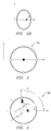
- the error signal When the measurement circuit 203 is balanced, the error signal has a virtually-circular trajectory within the IQ space and is centered on the origin of the IQ space. Deviations by from a circular trajectory within the IQ space are indicative of non-linear modes or IQ errors of the signal-generation circuit 201. If an IQ error is present, the signal is represented in the IQ space by an ellipse rather than by a circle, since there is a mismatch between the gain of the signal-generation circuit 201 on the I channel and the gain of the signal-generation circuit 201 on the Q channel. Non-linear modes can result from, for example, saturation of the PA 104, which compresses the circle, producing a trajectory having an elliptical component.
- the error signal has no time-varying component (i.e., the amplitude of is constant).
- inexpensive bridge circuitry that is not necessarily ultra-linear can be used in the measurement circuit 203 without introducing undesirable measurement biases that cannot be distinguished from non-linearities of the signal-generation circuit 201.
- ⁇ det is demodulated by a demodulation element 214 using the conjugate of a signal 218 output by the input-signal-generation circuit 202.
- the signal 218 is related to the conjugate of x i ( t ), except that the signal 218 does not include a DC offset.
- the signal 218 output by the input-signal-generation circuit 202 is phase adjusted, as represented by ⁇ m , so that the signal 218 and ⁇ det are both in phase with one another. Following the phase adjustment of the signal 218, a resulting phase-adjusted signal 220 is input to the demodulation element 214.
- a demodulated signal 222 output by the demodulation element 214 is low-pass filtered by a low-pass filter 216, thereby outputting a complex measurement ⁇ , which is a function of imbalance of the measurement circuit 203 and is preferably input to digital-signal-processing circuitry (not shown) that computes adjustments to the pre-distortion settings 112.
- the predistorted input signal is defined so that the amplitude of the signal is constant when the measurement circuit 203 is balanced, free from gain offsets, and the circuit 201 is linear. Because a constant-amplitude error signal does not stimulate non-linear modes within the diode 212, the effect of any non-ideal response of the diode 212 is thereby greatly reduced.
- the signal ⁇ det output by the diode 212 typically includes a constant component, a fundamental frequency that has the same fundamental frequency as x pd (t), and a second harmonic frequency that is twice the fundamental frequency of x pd (t).
- DFT digital Fourier transform
- the DFT at the fundamental frequency is used to adjust the pre-distortion parameters in order to cancel out any residual carrier signal within the signal .
- the DFT at the second harmonic frequency results a complex measurement that is proportional to elliptical deformations of the circular trajectory of the signal x i (t).
- the second-harmonic-frequency DFT is used to estimate non-linear modes that cause third-order inter-modulation distortion and also used to estimate IQ errors, including IQ gain imbalance and quadrature skew.
- the constant component of the input signal x i (t) is varied in terms of phase using PD 108 so that the average location of x pd (t) within the IQ space changes.
- the constant-component phase shift of x pd (t) is obtained by phase shifting within the measurement bridge (adjusting ⁇ m ), and then adjusting the signal path gain of PD 108 in order to balance the measurement circuit 203, thereby producing equal phase shift in and x pd . Since elliptical variations induced by IQ errors do not change with phase, the signal ⁇ det remains constant (once the measurement bridge is rebalanced).
- a Kalman filter can be used to estimate the non-linear and IQ error parameters from a set of second harmonic measurements measured from a plurality of input phase shifts.
- the PD 108 is preferably robust to uncertainty in the response of the diode 212, such as. For example, if the diode 212 does not exhibit a square-law response. If the diode 212 does not exhibit a square-law response, the primary effect is that a linear gain imbalance causes odd harmonics of the x pd (t) to appear in the signal ⁇ det . Such diode-induced harmonics of the signal x pd (t) are undesirable because they tend to mask any odd harmonics present in resulting from non-linearities within the PA 104. For this reason, only the fundamental and second harmonic frequencies of x pd are used.
- a model of the signal-generation circuit 201 is needed.
- a general model of the PD 108, the modulator 102, and the power amplifier 104 connected in series (collectively DMPA), as shown in FIG. 4, is: where G pd (x) is the gain of the PD 108.
- EQ (7) captures constant offsets (a -1 ), IQ impairments (a o , b o ), higher-order memoryless non-linearities (a k wherein k>0), and slew impairments (r k ). Even though EQ (7) has many coefficients, in general, the PD 108 will have only a few degrees of freedom.
- the PD 108 introduces a linear component and a memoryless third-order non-linearity.
- Gradient information can be obtained from the measurement circuit 203 that indicates adjustments to c 0 and c 2 that will improve the linearity of the DMPA.
- Four degrees of freedom are available to the PD: Re ⁇ c 0 ⁇ , Im ⁇ c 0 ⁇ , Re ⁇ c 2 ⁇ , and Im ⁇ c 2 ⁇ . ⁇ 0
- ⁇ is real and positive.
- the trajectories of x(t) and x LO (t) within the IQ space are shown in FIG. 3.
- ⁇ det When the DMPA is non-linear, the trajectory of y ORF (t) is compressed along one dimension of the IQ space, as shown in FIG. 4(b).
- the modes of ⁇ det are measured by demodulating using e- j ⁇ ps t and e - j ⁇ 2 ps t , respectively, then low-pass filtering. For example, wherein ⁇ ⁇ and ⁇ 2 ⁇ are first and second error measurements, respectively.
- the first and second error measurements provide useful information regarding the DMPA gain offsets and non-linearities.
- the second error measurement, ⁇ 2 ⁇ is If
- is small, ⁇ 2 ⁇ ⁇ 2 ⁇ 2 * ⁇ ⁇ and ⁇ 2 ⁇ are complex values.
- ⁇ ⁇ is a function of both the gain offset and the non-linearity, whereas ⁇ 2 ⁇ is a function of the non-linearity only.
- FIG. 5 illustrates another exemplary probing signal.
- the speed at which a probing signal 500 travels around the trajectory is altered from that shown in FIG. 3.
- a demodulation signal s demod (t) used with the signal 500 employs a time-varying weight to keep the center of the circle as the optimal balance point.
- the speed at which the signal 500 and the corresponding demodulation signal travel around the trajectory varies over time.
- the speed change is obtained by warping the time axis.
- the demodulation signal s demod (t) is weighted proportionally to the speed to eliminate measurement biases.
- the signal 500 can be represented by: wherein h t (t) is a function that warps the time axis. Time-axis warping alters the slew-rate and frequency-content of the signal 500, which highlights memory-effects within the DMPA.
- the demodulation signal s demod (t) must also be modified to account for speed variations.
- An alternative demodulation signal can be used in which the weight w(t) is replaced by a sampling function that comprises a train of delta functions. An interval between samples is adjusted to compensate for the temporal warping associated with h t (t). If the pre-warped sample rate is uniform and an integer multiple (N) of the probing signal frequency, the sample points are limited to N locations on the trajectory, as shown in FIG. 5. Thus, wherein T is the re-warped sampling interval of 2 ⁇ N/ ⁇ ps . The positions of the sampling points with respect to the trajectory are identical; however, the temporal spacing of the samples is, in general, no longer uniform.
- the estimate is then compared to the first error measurement ⁇ ⁇ .
- the estimate and the first error measurement ⁇ ⁇ are not equal; the difference is a measurement bias denoted by ⁇ bias .
- ⁇ X c and ⁇ y c ⁇ det .
- w(n) a weight assigned to sample n
- r(n) ⁇ det (n)
- R o E ⁇ ⁇ det ⁇
- ⁇ bias 0.
- One such set of signals is a sine wave whose frequency is altered, even reversed, every 2 ⁇ rotations around the trajectory. That is, frequency changes or reversals are permitted at a single location on the trajectory.
- EQ (43) only requires that the weighted average of the sample points be zero. That is, between samples, the probing signal is not constrained. In general, however, it is preferable to keep the detector error signal ⁇ det constant both at and between sample points in order to avoid stimulating any memory effects within the response of the diode 212.
- An alternative, and more general, approach for estimating the gain offsets is to estimate and subtract ⁇ bias from the first error measurement, ⁇ ⁇ .
- EQ (43) dictates that an estimate of R o be made. With an estimate of R o , direction reversals are not restricted to a single location on the trajectory. As a result, even a partial trajectory (i.e., an arc) can be used as a probing signal.
Landscapes
- Physics & Mathematics (AREA)
- Nonlinear Science (AREA)
- Engineering & Computer Science (AREA)
- Power Engineering (AREA)
- Amplifiers (AREA)
- Amplitude Modulation (AREA)
- Transmitters (AREA)
Abstract
Description























Claims (10)
- A method of reducing non-linearities of a circuit (201), the method comprising:providing an input signal, wherein the input signal comprises a constant component and a time-varying component;pre-distorting the input signal;inputting the pre-distorted input signal to the circuit (201);obtaining an output signal from the circuit (201);subtracting a carrier signal from the output signal, thereby yielding an error signal;determining an envelope of the error signal;demodulating the envelope of the error signal using a demodulating signal related to the input signal;adjusting parameters of the pre-distorted input signal with reference to the demodulated converted error signal, thereby causing an amplitude of the envelope of the error signal to approach a constant value.
- The method of claim 1, wherein the step of demodulating comprises performing a digital Fourier transform (DFT) on the envelope of the error signal.
- The method of claim 1 or 2, wherein the step of determining the envelope of the error signal is performed by a diode (124, 212).
- The method of one of the preceding claims, wherein the envelope of the error signal comprises:a constant component;a fundamental tone; anda second harmonic tone.
- The method of one of the preceding claims, wherein the constant value is zero.
- A system for reducing non-linearities comprising:wherein pre-distorter (108) parameter adjustments (112) cause an amplitude of the envelope of the error signal to approach a constant value, thereby reducing non-linearities of the signal-generation circuit (201).an input-signal-generation circuit (202) adapted to generate an input signal having a constant component and a time-varying component;a carrier-signal-generation circuit (106) adapted to generate a carrier signal;a signal-generation circuit (201) comprising:an input connected to the input-signal-generation circuit (202) and adapted to receive the input signal;a modulator (102) connected to the carrier-signal-generation circuit (106) and adapted to modulate the input signal with the carrier signal;an amplifier (104) connected to the modulator (102) and adapted to amplify the modulated input signal; andan output connected to the amplifier (104) and adapted to output the modulated amplified input signal;a pre-distorter (108) adapted to adjust signal parameters and connected to the signal-generation circuit (201);a measurement circuit (203) connected to the carrier-signal-generation circuit (106) and to the output and adapted to yield an envelope of an error signal, the envelope comprising a function of an imbalance of the measurement circuit (203); and
- The system of claim 6, wherein the measurement circuit (203) comprises a diode (124, 212).
- The system of claim 7, wherein the diode (124, 212) yields the envelope of the error signal.
- The system of one of claims 6 to 8, wherein the carrier signal and the output. signal are aligned as to gain and at least one of phase and time.
- The system of one of claims 6 to 9, wherein the constant value is zero.
Applications Claiming Priority (2)
| Application Number | Priority Date | Filing Date | Title |
|---|---|---|---|
| US10/084,702 US6566948B1 (en) | 2002-02-26 | 2002-02-26 | Method and system for reducing non-linearities |
| US84702 | 2002-02-26 |
Publications (2)
| Publication Number | Publication Date |
|---|---|
| EP1345319A2 true EP1345319A2 (en) | 2003-09-17 |
| EP1345319A3 EP1345319A3 (en) | 2005-07-06 |
Family
ID=22186678
Family Applications (1)
| Application Number | Title | Priority Date | Filing Date |
|---|---|---|---|
| EP02023149A Withdrawn EP1345319A3 (en) | 2002-02-26 | 2002-10-15 | Method and system for reducing non-linearities |
Country Status (3)
| Country | Link |
|---|---|
| US (1) | US6566948B1 (en) |
| EP (1) | EP1345319A3 (en) |
| JP (1) | JP2003273753A (en) |
Families Citing this family (22)
| Publication number | Priority date | Publication date | Assignee | Title |
|---|---|---|---|---|
| EP1528779A1 (en) * | 2003-10-29 | 2005-05-04 | Nuovotel Properties A.V.V. | System and method for frequency modulation in a modem |
| US7856105B2 (en) * | 2006-03-09 | 2010-12-21 | Andrew Llc | Apparatus and method for processing of amplifier linearization signals |
| US7755425B2 (en) * | 2006-04-10 | 2010-07-13 | Telefonaktiebolaget L M Ericsson (Publ) | Method and apparatus for reducing frequency memory effects in RF power amplifiers |
| ATE529944T1 (en) * | 2006-06-27 | 2011-11-15 | Ericsson Telefon Ab L M | SWITCHING POWER GAIN |
| US8344808B2 (en) * | 2008-03-31 | 2013-01-01 | Javelin Semiconductor, Inc. | Non-linear capacitance compensation |
| US8787850B2 (en) | 2008-03-31 | 2014-07-22 | Avago Technologies General Ip (Singapore) Pte. Ltd. | Compensating for non-linear capacitance effects in a power amplifier |
| US8219049B2 (en) * | 2008-03-31 | 2012-07-10 | Javelin Semiconductor, Inc. | Generating a process and temperature tracking bias voltage |
| US7872528B2 (en) * | 2008-04-10 | 2011-01-18 | Javelin Semiconductor, Inc. | Providing pre-distortion to an input signal |
| KR20100019947A (en) | 2008-08-11 | 2010-02-19 | 엘지전자 주식회사 | Method of transmitting information in wireless communication system |
| KR101603338B1 (en) | 2008-08-11 | 2016-03-15 | 엘지전자 주식회사 | Method and apparatus of transmitting information in wireless communication system |
| KR101571566B1 (en) | 2008-08-11 | 2015-11-25 | 엘지전자 주식회사 | Method of transmitting control signal in wireless communication system |
| KR101225920B1 (en) | 2008-11-14 | 2013-01-24 | 엘지전자 주식회사 | Method and apparatus for information transmission in wireless communication system |
| KR101243508B1 (en) | 2008-11-14 | 2013-03-20 | 엘지전자 주식회사 | Method and apparatus for signal transmission in wireless communication system |
| KR20100091876A (en) | 2009-02-11 | 2010-08-19 | 엘지전자 주식회사 | Ue behavior for multi-antenna transmission |
| WO2010136114A1 (en) * | 2009-05-29 | 2010-12-02 | University College Dublin - National University Of Ireland, Dublin | Digital predistorter for rf power amplifiers |
| US8354884B2 (en) * | 2009-11-25 | 2013-01-15 | Powerwave Technologies, Inc. | Measurement and correction of residual nonlinearities in a digitally predistorted power amplifier |
| CN102143107B (en) | 2011-02-25 | 2013-10-09 | 华为技术有限公司 | Method and device for realizing pre-distortion of digital baseband |
| US8779851B2 (en) * | 2012-05-15 | 2014-07-15 | Integrated Device Technology, Inc. | Linearizing a power amplifier |
| US9001928B2 (en) * | 2013-03-28 | 2015-04-07 | Texas Instruments Incorporated | Transmitter first/second digital predistortion and first/second adaption circuitry with feedback |
| US9819412B1 (en) * | 2016-05-04 | 2017-11-14 | Inphi Corporation | Transmitter gain imbalance and skew optimization for coherent transmitters |
| US9998216B2 (en) * | 2016-05-09 | 2018-06-12 | Fujitsu Limited | Skew measurement in an optical coherent transponder |
| US20260074944A1 (en) * | 2024-09-08 | 2026-03-12 | Tp-Link Systems Inc. | Wireless communication device and method for iq calibration |
Family Cites Families (9)
| Publication number | Priority date | Publication date | Assignee | Title |
|---|---|---|---|---|
| US5049832A (en) | 1990-04-20 | 1991-09-17 | Simon Fraser University | Amplifier linearization by adaptive predistortion |
| US5420536A (en) | 1993-03-16 | 1995-05-30 | Victoria University Of Technology | Linearized power amplifier |
| US5650758A (en) | 1995-11-28 | 1997-07-22 | Radio Frequency Systems, Inc. | Pipelined digital predistorter for a wideband amplifier |
| US5742201A (en) | 1996-01-30 | 1998-04-21 | Spectrian | Polar envelope correction mechanism for enhancing linearity of RF/microwave power amplifier |
| JPH1022844A (en) * | 1996-07-05 | 1998-01-23 | Fujitsu Ltd | Nonlinear distortion detection circuit and nonlinear distortion compensation circuit of transmitter |
| US6232835B1 (en) * | 1998-02-13 | 2001-05-15 | Nortel Networks Limited | System and method of linearizing the gain error of a power amplifier |
| US6236837B1 (en) * | 1998-07-30 | 2001-05-22 | Motorola, Inc. | Polynomial Predistortion linearizing device, method, phone and base station |
| ATE278786T1 (en) * | 1999-06-22 | 2004-10-15 | Consejo Superior Investigacion | GENETIC CAScade-regulated expression of cloned genes |
| ATE522023T1 (en) * | 2000-01-07 | 2011-09-15 | Powerwave Technologies Inc | CARRIER SUPPRESSION MECHANISM FOR A SAMPLING DETECTOR FOR MEASURING AND CORRECTING THE DISTORTION OF THE RF POWER AMPLIFIER |
-
2002
- 2002-02-26 US US10/084,702 patent/US6566948B1/en not_active Expired - Lifetime
- 2002-10-15 EP EP02023149A patent/EP1345319A3/en not_active Withdrawn
-
2003
- 2003-02-25 JP JP2003046999A patent/JP2003273753A/en active Pending
Also Published As
| Publication number | Publication date |
|---|---|
| EP1345319A3 (en) | 2005-07-06 |
| JP2003273753A (en) | 2003-09-26 |
| US6566948B1 (en) | 2003-05-20 |
Similar Documents
| Publication | Publication Date | Title |
|---|---|---|
| US6566948B1 (en) | Method and system for reducing non-linearities | |
| EP1224733B1 (en) | Adaptive linearization of power amplifiers | |
| EP0598585B1 (en) | Automatic calibration of the quadrature balance within a cartesian amplifier | |
| US6934341B2 (en) | Method and apparatus for plurality signal generation | |
| US6771709B2 (en) | System and method for direct transmitter self-calibration | |
| EP1382115B1 (en) | Automatic optimization of linearity for envelope feedback rf amplifier linearization | |
| US6987954B2 (en) | Feedback compensation detector for a direct conversion transmitter | |
| RU2336628C2 (en) | Device and method of amplifier pre-distortion and autocalibration | |
| US8326239B1 (en) | Power amplifier linearization using digital predistortion | |
| JP2513289B2 (en) | Modulator | |
| US4878030A (en) | Linearizer for microwave amplifier | |
| US8442460B2 (en) | Method for compensating signal distortions in composite amplifiers | |
| US8385458B2 (en) | Signal processing circuit and signal processing method | |
| US20030184374A1 (en) | Type-based baseband predistorter function estimation technique for non-linear circuits | |
| US20090054016A1 (en) | Apparatus and Method for Adaptive Cartesian Transmitter Linearization and Wireless Transmitter Employing the Same | |
| US20100074367A1 (en) | Adaptive combiner error calibration algorithms in all-digital outphasing transmitter | |
| US20040166813A1 (en) | Cartesian loop systems with digital processing | |
| US9344041B2 (en) | Polar amplification transmitter distortion reduction | |
| US20090156143A1 (en) | Power control loop, transmitter with the power control loop and method for controlling output power of a transmitter device | |
| JP6340207B2 (en) | Nonlinear distortion detector and distortion compensation power amplifier | |
| CN112511175A (en) | IQ mismatch estimation circuit, zero IF transmitter and method thereof | |
| EP1819040B1 (en) | Distortion compensating apparatus and method | |
| EP1573903B1 (en) | Phase-error based signal alignment | |
| JP3144649B2 (en) | Distortion compensated quadrature modulator | |
| JPH0531326B2 (en) |
Legal Events
| Date | Code | Title | Description |
|---|---|---|---|
| PUAI | Public reference made under article 153(3) epc to a published international application that has entered the european phase |
Free format text: ORIGINAL CODE: 0009012 |
|
| AK | Designated contracting states |
Kind code of ref document: A2 Designated state(s): AT BE BG CH CY CZ DE DK EE ES FI FR GB GR IE IT LI LU MC NL PT SE SK TR |
|
| AX | Request for extension of the european patent |
Extension state: AL LT LV MK RO SI |
|
| PUAL | Search report despatched |
Free format text: ORIGINAL CODE: 0009013 |
|
| AK | Designated contracting states |
Kind code of ref document: A3 Designated state(s): AT BE BG CH CY CZ DE DK EE ES FI FR GB GR IE IT LI LU MC NL PT SE SK TR |
|
| AX | Request for extension of the european patent |
Extension state: AL LT LV MK RO SI |
|
| 17P | Request for examination filed |
Effective date: 20051209 |
|
| AKX | Designation fees paid |
Designated state(s): DE GB |
|
| RAP1 | Party data changed (applicant data changed or rights of an application transferred) |
Owner name: AGILENT TECHNOLOGIES, INC. |
|
| STAA | Information on the status of an ep patent application or granted ep patent |
Free format text: STATUS: THE APPLICATION IS DEEMED TO BE WITHDRAWN |
|
| 18D | Application deemed to be withdrawn |
Effective date: 20080503 |