US6566948B1 - Method and system for reducing non-linearities - Google Patents

Method and system for reducing non-linearities Download PDF

Info

Publication number
US6566948B1
US6566948B1 US10/084,702 US8470202A US6566948B1 US 6566948 B1 US6566948 B1 US 6566948B1 US 8470202 A US8470202 A US 8470202A US 6566948 B1 US6566948 B1 US 6566948B1
Authority
US
United States
Prior art keywords
signal
envelope
input signal
generation circuit
circuit
Prior art date
Legal status (The legal status is an assumption and is not a legal conclusion. Google has not performed a legal analysis and makes no representation as to the accuracy of the status listed.)
Expired - Lifetime
Application number
US10/084,702
Inventor
Richard Neil Braithwaite
Current Assignee (The listed assignees may be inaccurate. Google has not performed a legal analysis and makes no representation or warranty as to the accuracy of the list.)
Keysight Technologies Inc
Original Assignee
Agilent Technologies Inc
Priority date (The priority date is an assumption and is not a legal conclusion. Google has not performed a legal analysis and makes no representation as to the accuracy of the date listed.)
Filing date
Publication date
Application filed by Agilent Technologies Inc filed Critical Agilent Technologies Inc
Priority to US10/084,702 priority Critical patent/US6566948B1/en
Assigned to AGILENT TECHNOLOGIES, INC. reassignment AGILENT TECHNOLOGIES, INC. ASSIGNMENT OF ASSIGNORS INTEREST (SEE DOCUMENT FOR DETAILS). Assignors: BRAITHWAITE, RICHARD NEIL
Priority to EP02023149A priority patent/EP1345319A3/en
Priority to JP2003046999A priority patent/JP2003273753A/en
Application granted granted Critical
Publication of US6566948B1 publication Critical patent/US6566948B1/en
Assigned to KEYSIGHT TECHNOLOGIES, INC. reassignment KEYSIGHT TECHNOLOGIES, INC. ASSIGNMENT OF ASSIGNORS INTEREST (SEE DOCUMENT FOR DETAILS). Assignors: AGILENT TECHNOLOGIES, INC.
Anticipated expiration legal-status Critical
Expired - Lifetime legal-status Critical Current

Links

Images

Classifications

    • HELECTRICITY
    • H03ELECTRONIC CIRCUITRY
    • H03FAMPLIFIERS
    • H03F1/00Details of amplifiers with only discharge tubes, only semiconductor devices or only unspecified devices as amplifying elements
    • H03F1/32Modifications of amplifiers to reduce non-linear distortion
    • H03F1/3241Modifications of amplifiers to reduce non-linear distortion using predistortion circuits
    • H03F1/3247Modifications of amplifiers to reduce non-linear distortion using predistortion circuits using feedback acting on predistortion circuits

Definitions

  • the present invention relates in general to the field of signal generation, and in particular, by way of example but not limitation, to reduction of non-linearities in signal-generation circuits.
  • a major objective of the present invention is to reduce non-linearities in signal-generation circuits.
  • Attempts to improve the linearity of a series combination of a modulator and power amplifier include: (a) choosing components that are more linear; and (b) using linearization techniques such as, for example, feedback, feedforward, and pre-distortion.
  • Feedback generally refers to feeding back at least a part of a signal to a delayed version of the signal in order to correct the signal substantially in real time.
  • Feedforward generally refers to correcting a signal in advance so the future signals are corrected. Because components that exhibit greater linearity are often more expensive than components that exhibit lesser linearity, linearization techniques that correct non-linearities of the less-linear components have been pursued.
  • Feedback linearization generally has two forms: 1) polar; and 2) Cartesian. Linearization can be applied to either a base-band signal, an IF (intermediate-frequency) signal (if one exists), or a radio-frequency (RF) signal. In general, feedback loop delays tend to limit the available signal bandwidth and can lead to instability if bandwidth restrictions are exceeded.
  • Feedforward linearization operates by measuring distortion from non-linearities, delaying a main signal, and subtracting the distortion from the main signal using the measured distortion. Feedforward linearization tends to be used for reducing effects of non-linearities in RF components, such as, for example, a PA. Modulator errors are not typically corrected using feedforward linearization. Feedforward linearization performance is typically limited by the quality of a second, reference amplifier, used to amplify the measured distortion. Disadvantages of using feedforward compensation include expense and the need for precise balances between reference and signal paths in order to obtain acceptable performance.
  • Pre-distortion linearization involves the introduction of non-linearities into a signal path.
  • the non-linearities are then used to counteract non-linearities present in the original components, such as, for example, the modulator and the PA.
  • An objective of pre-distortion is to keep constant the gain of the series combination of a pre-distorter (PD), the modulator, and the PA, despite instantaneous signal power-level variations due to time-varying (e.g., amplitude-modulation (AM)) components of the signal.
  • Pre-distortion linearization can be applied anywhere along the signal path; however, in certain applications, pre-distortion linearization of the base-band or of the RF signal might be preferred.
  • Pre-distortion linearization typically compensates for the modulator and PA non-linearities by modeling as a parametric function a time-varying inverse of the non-linear gain of the system. Pre-distortion parameters that minimize the output distortion are also usually estimated. When the pre-distortion is perfect, the parameters of the inverse non-linear gain are identical to those minimizing the output distortion. Adaptive estimation of the pre-distortion parameters is desirable because the gain can drift over time.
  • the adaptive parameter estimation typically requires that the gain variations be measured accurately. Inaccurate measurements of the gain variations can bias the parameter estimation, thereby impairing the performance of pre-distortion linearization.
  • the present invention provides a method and system for improving the linearity of circuits such as signal-generation circuits using a measurement circuit that is not required to be ultra-linear and is therefore less expensive than other approaches.
  • a time-varying signal with an AM component is input to a circuit in order to excite non-linearities of the circuit.
  • the measurement circuit is balanced to remove the AM component so that the resulting signal does not excite any non-linearities of the measurement circuit. Any such non-linearities of the measurement circuit are minimized by extracting a portion of the signal that passes through the circuit. The extracted portion does not have a substantial time-varying component.
  • non-linearities of the measurement circuit are not excited, while non-linearities of the circuit are excited and can therefore be measured and subsequently corrected.
  • a method of reducing non-linearities of a circuit includes providing and pre-distorting an input signal.
  • the input signal includes a constant component and a time-varying component.
  • the pre-distorted input signal is input to the circuit and an output signal is obtained from the circuit.
  • a carrier signal is subtracted from the output signal, thereby yielding an error signal.
  • An error signal envelope is determined and is demodulated using a demodulating signal related to the input signal.
  • the parameters of the pre-distorted input signal are adjusted with reference to the demodulated converted error signal, thereby causing an amplitude of the error signal envelope to approach a constant value.
  • a system for reducing non-linearities includes an input-signal-generation circuit and a carrier-signal-generation circuit.
  • the signal-generation circuit is adapted to generate an input signal having a constant component and a time-varying component.
  • the carrier-signal-generation circuit is adapted to generate a carrier signal.
  • the circuit includes an input connected to the input-signal-generation circuit and adapted to receive the input signal and a modulator connected to the carrier-signal-generation circuit and adapted to modulate the input signal with the carrier signal.
  • the circuit also includes an amplifier, connected to the modulator, adapted to amplify the modulated input signal. An output is connected to the amplifier and is adapted to output the modulated amplified input signal.
  • the system includes a pre-distorter that is adapted to adjust signal parameters.
  • the pre-distorter is connected to the circuit.
  • the measurement circuit is adapted to yield an envelope of an error signal.
  • the envelope comprises a function of an imbalance of the measurement circuit. Pre-distortion parameter adjustments are used to cause an amplitude of an envelope of the error signal to approach a constant value, thereby reducing non-linearities of the circuit.
  • FIG. 1 is a block diagram of a linearization circuit in accordance with teachings of the present invention
  • FIG. 2 is a block diagram of a linearization circuit in accordance with teachings of the present invention.
  • FIG. 3 is a graph of an exponential probing signal and local oscillator signal in accordance with teachings of the present invention.
  • FIG. 4 ( a ) is a graph of a local oscillator signal and an output signal of a signal-generation circuit having a gain offset
  • FIG. 4 ( b ) is a graph of a local oscillator signal and an output signal of a signal-generation circuit that is non-linear;
  • FIG. 5 is a graph of an exemplary probing signal
  • FIG. 6 is graph of a trajectory of a detected error signal of a linear DMPA that has gain offsets.
  • FIG. 1 is a block diagram of a linearization circuit 100 in accordance with teachings of the present invention.
  • the linearization circuit 100 which has a base-band input signal x(t), could be, for example, an Agilent ESG-D Falcon signal generator.
  • the base-band input signal x(t) comprises a quadrature pair of base-band signals, denoted by I and Q (i.e., in-phase and quadrature components), respectively.
  • An output of the linearization circuit 100 is an RF signal denoted by ⁇ tilde over (y) ⁇ RF (t).
  • a modulator 102 and a power amplifier (PA) 104 are arranged in series.
  • a local oscillator (LO) 106 provides an RF input signal ⁇ tilde over (x) ⁇ LO (t) to the modulator 102 .
  • LO local oscillator
  • pre-distortion can be applied anywhere along the signal path. Even though pre-distortion can be applied anywhere along the signal path, such as, for example, prior to the modulator 102 , on the RF signal path between the modulator 102 and the PA 104 , or after the PA 104 , pre-distortion of the base-band input x(t) is often preferred because of ease of implementation.
  • a pre-distorter (PD) 108 distorts x(t) and then provides a pre-distorted signal to a digital-to-analog converter (DAC) 110 , which outputs to the modulator 102 .
  • Pre-distortion settings 112 can be made to the PD 108 via a controller 114 . The pre-distortion settings 112 allow adjustments to be made to parameters of the PD 108 in order to improve linearity of the linearization circuit 100 .
  • An output signal of the modulator 102 is input to the PA 104 .
  • the controller 114 is also coupled to an analog-to-digital-converter/coefficient calculator (ADC/coefficient calculator) block 116 , to a gain-adjustment block 118 , and to a phase-adjustment block 120 in order to make adjustments to any of the blocks 116 , 118 , or 120 .
  • ADC/coefficient calculator analog-to-digital-converter/coefficient calculator
  • the output signal ⁇ tilde over (y) ⁇ RF (t) is fed to an output device, such as, for example, an antenna, and also to the gain-adjustment block 118 .
  • the output of the gain-adjustment block 118 is fed to a combiner 122 , which also receives the inverse of the output of the LO 106 , after phase adjustment by the phase-adjustment block 120 , as an input.
  • the gain-adjustment block 118 and the phase-adjustment block 120 are used to align the gain and phase of the output signal and of the output of the modulator 102 so that each of the signals is of similar phase and average power.
  • the combiner 122 subtracts the phase-adjusted output of the LO 106 from the gain-adjusted output of the linearization circuit 100 .
  • the output of the combiner 122 is fed to a diode 124 , which produces an envelope signal of the output of the combiner 122 .
  • the diode 124 is output to the ADC/coefficient calculator 116 , which makes adjustments to the PD settings 112 in order to improve the linearity of the linearization circuit 100 .
  • the pre-distortion settings 112 of the PD 108 are adjusted manually.
  • the pre-distortion settings 112 are typically adjusted via a one-time procedure.
  • 1 Higher complexity pre-distortion involves automatic adjustment of the pre-distortion settings 112 .
  • Automatic adjustment of the pre-distortion settings 112 can be grouped into two general classes: 1) off-line calibration, and 2) on-line adaptation.
  • Off-line calibration uses known input signals to determine adjustments to the pre-distortion settings 112 . In off-line calibration, use of the linearization circuit 100 is suspended. In contrast, in on-line adaptation, the settings 112 are adjusted while the linearization circuit 100 is in use and the input signal x(t) is being used.
  • gain error of the linearization circuit 100 between the input signal x(t) and the RF output signal ⁇ tilde over (y) ⁇ RF (t) is measured.
  • a tuning algorithm of the controller 114 relates adjustments made to the pre-distortion settings 112 to the measured gain error between the input signal x(t) and the RF output signal ⁇ tilde over (y) ⁇ RF (t).
  • An iterative process can be used to adjust the pre-distortion settings 112 of the PD 108 and, if the iterative process converges, the linearity of the linearization circuit 100 improves.
  • pre-distortion is used to reduce the non-linearities of the linearization circuit 100 on a signal path that includes the modulator 102 and the PA 104 .
  • the pre-distortion is applied to the signal path prior to the conversion of the signal from digital to analog by the DAC 110 .
  • the pre-distortion can be applied anywhere along the signal path.
  • Parameters of the pre-distortion function are preferably estimated via a calibration procedure that uses the input signal x(t). The estimated parameters are then fixed and are used to compensate for gain fluctuations associated with an arbitrary signal of similar average power to the input signal x(t).
  • linearity of devices that use modulators and amplifiers to convert base-band signals to RF can be improved.
  • embodiments of the present invention eliminate offsets between desired gain and actual gain.
  • the PD 108 can be made to introduce a non-linearity into the signal path of the linearization circuit 100 in order to compensate for subsequently-introduced non-linearities by, for example, the modulator 102 and the PA 104 .
  • the PD 108 is adjusted by inputting the signal x(t) (after pre-distortion) to the modulator 102 and measuring an error signal. As the pre-distortion reduces the gain offsets and improves the linearity of the linearization circuit 100 , the error signal converges towards a constant value.
  • Selection of an appropriate input signal x(t) helps to ensure that non-linear modes within the modulator 102 and the PA 104 are stimulated and also enables extraction of a portion of the output signal ⁇ tilde over (y) ⁇ RF (t) that does not stimulate non-linear modes of any of the blocks 118 or 120 or of the combiner 122 or diode 124 .
  • accurate, bias-free parameter estimates can be obtained using inexpensive, relatively non-linear, components.
  • the input signal x(t) comprises a constant (i.e., DC) component and a time-varying (e.g., complex exponential) component.
  • the input signal x(t) also referred to as a probing signal, can be represented by a circle in the in-phase-quadrature plane that is offset from the origin by a constant component.
  • the complex-exponential component of the input signal x(t) introduces a time-varying (e.g., AM) signal component.
  • FIG. 2 is a detailed block diagram of a linearization circuit 200 in accordance with teachings of the present invention.
  • the linearization circuit 200 includes a signal-generation circuit 201 , an input-signal-generation circuit 202 , and a measurement circuit 203 .
  • the input-signal-generation circuit 202 generates an input signal x i (t), which, in the embodiment represented in FIG. 2, includes a constant offset on the I-channel plus a weighted disturbance such that:
  • s mod (t) is a time-varying signal and ⁇ is a modulation index.
  • the signal s mod (t) performs two principal functions: (1) s mod (t) stimulates non-linear modes of the modulator 102 and the PA 104 by varying an amplitude of the input signal x i (t) and 2) s mod (t) disrupts an instantaneous balance of the measurement circuit 203 , which can also be referred to as am measurement bridge circuit, so that optimal settings of the PD 108 can be determined.
  • An RF output signal of the circuit 201 can be described by:
  • y ORF (t) is a complex baseband signal
  • ⁇ LO is the carrier frequency in rad/sec
  • j ⁇ square root over ( ⁇ 1) ⁇ .
  • Other signals shown in FIG. 4 are ⁇ tilde over (x) ⁇ LO (t) (i.e., the modulating, or LO, signal), ⁇ tilde over (x) ⁇ mpd (t) (i.e., a pre-distorted and modulated input signal), and ⁇ tilde over ( ⁇ ) ⁇ RF (t) (i.e., an RF error signal), wherein:
  • x LO (t), x mpd (t), and ⁇ RF (t) are the respective complex baseband signals.
  • the LO signal ⁇ tilde over (x) ⁇ LO (t) output by the LO 106 is input to the modulator 102 , which up-converts a pre-distorted input signal ⁇ tilde over (x) ⁇ pd (t) to RF, thereby yielding the modulated pre-distorted input signal ⁇ tilde over (x) ⁇ mpd (t).
  • a phase-shifted version of the LO signal ⁇ tilde over (x) ⁇ LO (t) is subtracted from a gain-adjusted sample of the output signal ⁇ tilde over (y) ⁇ ORF (t), thereby yielding the error signal ⁇ tilde over ( ⁇ ) ⁇ RF (t).
  • the error signal ⁇ tilde over ( ⁇ ) ⁇ RF (t) is output by a combiner 210 of the measurement circuit 203 .
  • the measurement circuit 203 includes two paths, a reference path 206 and an output path 208 , which are nominally balanced in terms of amplitude and are 180 degrees offset in phase from one another.
  • the reference path 206 carries a replica of the signal ⁇ tilde over (x) ⁇ LO (t).
  • the output path 208 carries a replica of the output signal ⁇ tilde over (y) ⁇ ORF (t).
  • a delay ⁇ m and an attenuation G attn are inserted along the reference path 206 and the output RF path 208 , respectively.
  • the signals on the reference path 206 and the output path 208 are thereby made coincident in time and of similar power levels at the combiner 210 in order to minimize power of the error signal ⁇ tilde over ( ⁇ ) ⁇ RF (t).
  • the error signal ⁇ tilde over ( ⁇ ) ⁇ RF (t) When the measurement circuit 203 is balanced, the error signal ⁇ tilde over ( ⁇ ) ⁇ RF (t) has a virtually-circular trajectory within the IQ space and is centered on the origin of the IQ space. Deviations by ⁇ tilde over (y) ⁇ ORF (t) from a circular trajectory within the IQ space are indicative of non-linear modes or IQ errors of the signal-generation circuit 201 . If an IQ error is present, the signal ⁇ tilde over (y) ⁇ ORF (t) is represented in the IQ space by an ellipse rather than by a circle, since there is a mismatch between the gain of the signal-generation circuit 201 on the I channel and the gain of the signal-generation circuit 201 on the Q channel.
  • Non-linear modes can result from, for example, saturation of the PA 104 , which compresses the circle, producing a trajectory having an elliptical component.
  • the error signal ⁇ tilde over ( ⁇ ) ⁇ RF (t) has no time-varying component (i.e., the amplitude of ⁇ tilde over ( ⁇ ) ⁇ RF (t) is constant).
  • inexpensive bridge circuitry that is not necessarily ultra-linear can be used in the measurement circuit 203 without introducing undesirable measurement biases that cannot be distinguished from non-linearities of the signal-generation circuit 201 .
  • An envelope ⁇ det of the error signal ⁇ tilde over ( ⁇ ) ⁇ RF (t) is obtained using a diode 212 .
  • the diode 212 is used to convert the error signal ⁇ tilde over ( ⁇ ) ⁇ RF (t) into a response that is a function of the amplitude of the error signal ⁇ tilde over ( ⁇ ) ⁇ RF (t).
  • the response of the diode 212 is ideally the absolute squared value of the amplitude of the signal ⁇ tilde over ( ⁇ ) ⁇ RF (t). Deviations from the ideal response have no significant deleterious effects on operation of embodiments of the present invention, because when the measurement circuit 203 is balanced, the signal ⁇ tilde over ( ⁇ ) ⁇ RF (t) includes substantially no time-varying component and therefore does not stimulate non-linearities of the measurement circuit 203 .
  • ⁇ det is demodulated by a demodulation element 214 using the conjugate of a signal 218 output by the input-signal-generation circuit 202 .
  • the signal 218 is related to the conjugate of x i (t), except that the signal 218 does not include a DC offset.
  • the signal 218 output by the input-signal-generation circuit 202 is phase adjusted, as represented by ⁇ m , so that the signal 218 and ⁇ det are both in phase with one another. Following the phase adjustment of the signal 218 , a resulting phase-adjusted signal 220 is input to the demodulation element 214 .
  • a demodulated signal 222 output by the demodulation element 214 is low-pass filtered by a low-pass filter 216 , thereby outputting a complex measurement ⁇ , which is a function of imbalance of the measurement circuit 203 and is preferably input to digital-signal-processing circuitry (not shown) that computes adjustments to the pre-distortion settings 112 .
  • the predistorted input signal ⁇ tilde over (x) ⁇ pd (t) is defined so that the amplitude of the signal ⁇ tilde over ( ⁇ ) ⁇ RF (t) is constant when the measurement circuit 203 is balanced, free from gain offsets, and the circuit 201 is linear. Because a constant-amplitude error signal does not stimulate non-linear modes within the diode 212 , the effect of any non-ideal response of the diode 212 is thereby greatly reduced.
  • the signal ⁇ det output by the diode 212 typically includes a constant component, a fundamental frequency that has the same fundamental frequency as x pd (t), and a second harmonic frequency that is twice the fundamental frequency of x pd (t).
  • DFT digital Fourier transform
  • the DFT at the fundamental frequency is used to adjust the pre-distortion parameters in order to cancel out any residual carrier signal within the signal ⁇ tilde over ( ⁇ ) ⁇ RF (t).
  • the DFT at the second harmonic frequency results a complex measurement that is proportional to elliptical deformations of the circular trajectory of the signal x i (t).
  • the second-harmonic-frequency DFT is used to estimate non-linear modes that cause third-order inter-modulation distortion and also used to estimate IQ errors, including IQ gain imbalance and quadrature skew.
  • the constant component of the input signal x i (t) is varied in terms of phase using PD 108 so that the average location of x pd (t) within the IQ space changes.
  • the constant-component phase shift of x pd (t) is obtained by phase shifting ⁇ tilde over (x) ⁇ LO (t ⁇ m ) within the measurement bridge (adjusting ⁇ m ), and then adjusting the signal path gain of PD 108 in order to balance the measurement circuit 203 , thereby producing equal phase shift in ⁇ tilde over (y) ⁇ attn , ⁇ tilde over (y) ⁇ ORF , ⁇ tilde over (x) ⁇ mpd and x pd .
  • a Kalman filter can be used to estimate the non-linear and IQ error parameters from a set of second harmonic measurements measured from a plurality of input phase shifts.
  • the PD 108 is preferably robust to uncertainty in the response of the diode 212 , such as. For example, if the diode 212 does not exhibit a square-law response. If the diode 212 does not exhibit a square-law response, the primary effect is that a linear gain imbalance causes odd harmonics of the x pd (t) to appear in the signal ⁇ det . Such diode-induced harmonics of the signal x pd (t) are undesirable because they tend to mask any odd harmonics present in ⁇ tilde over (y) ⁇ ORF (t) resulting from non-linearities within the PA 104 . For this reason, only the fundamental and second harmonic frequencies of x pd are used.
  • a model of the signal-generation circuit 201 is needed.
  • G pd (x) is the gain of the PD 108 .
  • EQ (7) captures constant offsets (a ⁇ 1 ), IQ impairments (a o , b o ), higher-order memoryless non-linearities (a k wherein k>0), and slew impairments (r k ). Even though EQ (7) has many coefficients, in general, the PD 108 will have only a few degrees of freedom.
  • a simple PD 108 with a gain offset and a power-related term can be represented by:
  • the PD 108 introduces a linear component and a memoryless third-order non-linearity.
  • Gradient information can be obtained from the measurement circuit 203 that indicates adjustments to c 0 and c 2 that will improve the linearity of the DMPA.
  • Four degrees of freedom are available to the PD: Re ⁇ c 0 ⁇ , Im ⁇ c 0 ⁇ , Re ⁇ c 2 ⁇ , and Im ⁇ c 2 ⁇ .
  • ( ⁇ 0 , ⁇ 2 ) is the gradient of the gain coefficient of the DMPA.
  • FIG. 3 is a graph of an exemplary signal x(t) and the carrier signal x LO (t) when s mod (t) is a complex exponential signal:
  • is real and positive.
  • the trajectories of x(t) and x LO (t) within the IQ space are shown in FIG. 3.
  • ⁇ det When the DMPA is non-linear, the trajectory of y ORF (t) is compressed along one dimension of the IQ space, as shown in FIG. 4 ( b ).
  • the modes of ⁇ det are measured by demodulating using e ⁇ j ⁇ ps t and e ⁇ j2 ⁇ pst , respectively, then low-pass filtering.
  • ⁇ ⁇ and ⁇ 2 ⁇ are first and second error measurements, respectively.
  • the first and second error measurements provide useful information regarding the DMPA gain offsets and non-linearities.
  • the second error measurement, F 2 ⁇ is
  • ⁇ 2 ⁇ ⁇ 2 ⁇ [ ⁇ 2 +( ⁇ 0 ⁇ 2 *+ ⁇ 2 ⁇ 0 *)] (22)
  • ⁇ ⁇ ⁇ [ ⁇ 0 ⁇ ( ⁇ 0 * ⁇ 1)+ ⁇ 2 *]+ ⁇ 3 ⁇ [2 ⁇ Re ⁇ 2 ⁇ + ⁇ 2 *] (23)
  • ⁇ ⁇ and ⁇ 2 ⁇ are complex values.
  • ⁇ ⁇ is a function of both the gain offset and the non-linearity
  • ⁇ 2 ⁇ is a function of the non-linearity only.
  • Variations to the complex exponential signal can be used to produce a class of probing signals that possess the desired property of making ⁇ det constant such that the DMPA is balanced and linear.
  • Three exemplary probing/demodulation signal pairs are presented hereinbelow, each of which is each based on the circular trajectory shown in FIG. 3 .
  • FIG. 5 illustrates another exemplary probing signal.
  • the speed at which a probing signal 500 travels around the trajectory is altered from that shown in FIG. 3.
  • a demodulation signal s demod (t) used with the signal 500 employs a time-varying weight to keep the center of the circle as the optimal balance point.
  • the speed at which the signal 500 and the corresponding demodulation signal travel around the trajectory varies over time.
  • the speed change is obtained by warping the time axis.
  • the demodulation signal s demod (t) is weighted proportionally to the speed to eliminate measurement biases.
  • the signal 500 can be represented by:
  • h t (t) is a function that warps the time axis.
  • Time-axis warping alters the slew-rate and frequency-content of the signal 500 , which highlights memory-effects within the DMPA.
  • the demodulation signal s demod (t) must also be modified to account for speed variations.
  • w(t) is a time-varying weight.
  • the term w(t) eliminates any bias in ⁇ ⁇ , thus keeping the center of the circle as the linear balance point.
  • a weight w(t) must be found that makes EQ (31) equal to zero over an observation interval [ 0 ,T]. If endpoints of the observation interval [ 0 ,T] are chosen such that
  • each point (differential arc segment) within the circular trajectory is given equal weight in determining the balance point.
  • An alternative demodulation signal can be used in which the weight w(t) is replaced by a sampling function that comprises a train of delta functions. An interval between samples is adjusted to compensate for the temporal warping associated with h t (t). If the pre-warped sample rate is uniform and an integer multiple (N) of the probing signal frequency, the sample points are limited to N locations on the trajectory, as shown in FIG. 5 . Thus,
  • T is the re-warped sampling interval of 2 ⁇ N/ ⁇ ps .
  • the positions of the sampling points with respect to the trajectory are identical; however, the temporal spacing of the samples is, in general, no longer uniform.
  • FIG. 6 illustrates a trajectory of a detected error signal of a linear DMPA that has gain offsets.
  • a sampled demodulation signal is generalized to allow the direction of travel to be reversed at any time while still maintaining the center of the circle as the balance point. As a result, a new class of probing signals is available, including those whose travel is isolated to an arc on the circle.
  • the demodulation signal has a sampled form.
  • the estimate is then compared to the first error measurement ⁇ ⁇ .
  • the estimate and the first error measurement ⁇ ⁇ are not equal; the difference is a measurement bias denoted by ⁇ bias .
  • w(n) is a weight assigned to sample n
  • r(n) ⁇ det (n)
  • R o E ⁇ det ⁇
  • x ⁇ ( n ) r ⁇ ( n ) ⁇ cos ⁇ [ ⁇ ps ⁇ ( n ) + ⁇ ⁇ ⁇ ⁇ ] - ⁇ ⁇ ⁇ x c ( 36 )
  • y ⁇ ( n ) r ⁇ ( n ) ⁇ sin ⁇ [ ⁇ ps ⁇ ( n ) + ⁇ ⁇ ⁇ ] - ⁇ ⁇ ⁇ y c ( 37 )
  • ⁇ bias R o N ⁇ ⁇ n ⁇ w ⁇ ( n ) ⁇ ⁇ - j ⁇ ⁇ ⁇ ps ⁇ ( n ) ( 43 )
  • ⁇ bias 0.
  • One such set of signals is a sine wave whose frequency is altered, even reversed, every 2 ⁇ rotations around the trajectory. That is, frequency changes or reversals are permitted at a single location on the trajectory.
  • EQ (43) only requires that the weighted average of the sample points be zero. That is, between samples, the probing signal is not constrained. In general, however, it is preferable to keep the detector error signal ⁇ det constant both at and between sample points in order to avoid stimulating any memory effects within the response of the diode 212 .
  • An alternative, and more general, approach for estimating the gain offsets is to estimate and subtract ⁇ bias from the first error measurement, ⁇ ⁇ .
  • EQ (43) dictates that an estimate of R o be made. With an estimate of R o , direction reversals are not restricted to a single location on the trajectory. As a result, even a partial trajectory (i.e., an arc) can be used as a probing signal.

Abstract

Non-linearities of signal-generation circuits that typically include a series arrangement of a modulator and a power amplifier are reduced by connecting a measurement circuit to an output of the signal-generation circuit and at another point along a signal path of the signal-generation circuit. A predistorted input signal is applied to an input of the signal-generation circuit. The pre-distorted signal includes a constant component and a time-varying component, such that the predistorted input signal excites non-linear modes of the signal-generation circuit. The measurement circuit is balanced so that a portion of the predistorted input signal that passes through the measurement circuit does not include a time-varying component and therefore does not excite non-linearities of the measurement circuit. Adjustments are made to the predistorted input signal in order to reduce non-linearities of the signal-generation circuit.

Description

BACKGROUND OF THE INVENTION
1. Technical Field of the Invention
The present invention relates in general to the field of signal generation, and in particular, by way of example but not limitation, to reduction of non-linearities in signal-generation circuits. A major objective of the present invention is to reduce non-linearities in signal-generation circuits.
2. Description of Related Art
Attempts to improve the linearity of a series combination of a modulator and power amplifier (PA) include: (a) choosing components that are more linear; and (b) using linearization techniques such as, for example, feedback, feedforward, and pre-distortion. Feedback generally refers to feeding back at least a part of a signal to a delayed version of the signal in order to correct the signal substantially in real time. Feedforward generally refers to correcting a signal in advance so the future signals are corrected. Because components that exhibit greater linearity are often more expensive than components that exhibit lesser linearity, linearization techniques that correct non-linearities of the less-linear components have been pursued.
Feedback linearization generally has two forms: 1) polar; and 2) Cartesian. Linearization can be applied to either a base-band signal, an IF (intermediate-frequency) signal (if one exists), or a radio-frequency (RF) signal. In general, feedback loop delays tend to limit the available signal bandwidth and can lead to instability if bandwidth restrictions are exceeded.
Feedforward linearization operates by measuring distortion from non-linearities, delaying a main signal, and subtracting the distortion from the main signal using the measured distortion. Feedforward linearization tends to be used for reducing effects of non-linearities in RF components, such as, for example, a PA. Modulator errors are not typically corrected using feedforward linearization. Feedforward linearization performance is typically limited by the quality of a second, reference amplifier, used to amplify the measured distortion. Disadvantages of using feedforward compensation include expense and the need for precise balances between reference and signal paths in order to obtain acceptable performance.
Pre-distortion linearization involves the introduction of non-linearities into a signal path. The non-linearities are then used to counteract non-linearities present in the original components, such as, for example, the modulator and the PA. An objective of pre-distortion is to keep constant the gain of the series combination of a pre-distorter (PD), the modulator, and the PA, despite instantaneous signal power-level variations due to time-varying (e.g., amplitude-modulation (AM)) components of the signal. Pre-distortion linearization can be applied anywhere along the signal path; however, in certain applications, pre-distortion linearization of the base-band or of the RF signal might be preferred.
Pre-distortion linearization typically compensates for the modulator and PA non-linearities by modeling as a parametric function a time-varying inverse of the non-linear gain of the system. Pre-distortion parameters that minimize the output distortion are also usually estimated. When the pre-distortion is perfect, the parameters of the inverse non-linear gain are identical to those minimizing the output distortion. Adaptive estimation of the pre-distortion parameters is desirable because the gain can drift over time.
The adaptive parameter estimation typically requires that the gain variations be measured accurately. Inaccurate measurements of the gain variations can bias the parameter estimation, thereby impairing the performance of pre-distortion linearization.
An inherent problem with adaptive approaches to linearization is that the system being linearized cannot distinguish distortion induced by non-linearities of, for example, the modulator or the PA within the signal path from non-linearities induced by measurement components used to measure the non-linearities within the signal path. As a result, many currently-known adaptive pre-distortion linearization approaches require ultra-linear measurement components. These ultra-linear measurements are often prohibitively expensive.
From the foregoing it can be seen that non-linearities of signal-generation circuits have required ultra-linear measurement components, which are often prohibitively expensive. What is needed is a method and system for reducing non-linearities in signal-generation circuits that improve the linearity of such circuits without requiring ultra-linear measurement components.
SUMMARY OF THE INVENTION
The present invention provides a method and system for improving the linearity of circuits such as signal-generation circuits using a measurement circuit that is not required to be ultra-linear and is therefore less expensive than other approaches. A time-varying signal with an AM component is input to a circuit in order to excite non-linearities of the circuit. The measurement circuit is balanced to remove the AM component so that the resulting signal does not excite any non-linearities of the measurement circuit. Any such non-linearities of the measurement circuit are minimized by extracting a portion of the signal that passes through the circuit. The extracted portion does not have a substantial time-varying component. Thus, non-linearities of the measurement circuit are not excited, while non-linearities of the circuit are excited and can therefore be measured and subsequently corrected.
In an embodiment of the present invention, a method of reducing non-linearities of a circuit includes providing and pre-distorting an input signal. The input signal includes a constant component and a time-varying component. The pre-distorted input signal is input to the circuit and an output signal is obtained from the circuit. A carrier signal is subtracted from the output signal, thereby yielding an error signal. An error signal envelope is determined and is demodulated using a demodulating signal related to the input signal. The parameters of the pre-distorted input signal are adjusted with reference to the demodulated converted error signal, thereby causing an amplitude of the error signal envelope to approach a constant value.
In another embodiment of the present invention, a system for reducing non-linearities includes an input-signal-generation circuit and a carrier-signal-generation circuit. The signal-generation circuit is adapted to generate an input signal having a constant component and a time-varying component. The carrier-signal-generation circuit is adapted to generate a carrier signal. The circuit includes an input connected to the input-signal-generation circuit and adapted to receive the input signal and a modulator connected to the carrier-signal-generation circuit and adapted to modulate the input signal with the carrier signal. The circuit also includes an amplifier, connected to the modulator, adapted to amplify the modulated input signal. An output is connected to the amplifier and is adapted to output the modulated amplified input signal. The system includes a pre-distorter that is adapted to adjust signal parameters. The pre-distorter is connected to the circuit. There is also a measurement circuit connected to the carrier-signal-generation circuit and to the output. The measurement circuit is adapted to yield an envelope of an error signal. The envelope comprises a function of an imbalance of the measurement circuit. Pre-distortion parameter adjustments are used to cause an amplitude of an envelope of the error signal to approach a constant value, thereby reducing non-linearities of the circuit.
The above-described and other features of the present invention are explained in detail below with reference to illustrative examples shown in the accompanying Drawings. Those of ordinary skill in the art will appreciate that the described embodiments are provided for purposes of illustration and understanding and that numerous equivalent embodiments are also contemplated in this patent application. Furthermore, the present invention provides embodiments with other features and advantages in addition to or instead of those discussed above. Many of the features and advantages are apparent from the description below with reference to the following drawings:
BRIEF DESCRIPTION OF THE DRAWINGS
A more complete understanding of the present invention can be achieved by reference to the following Detailed Description when taken in conjunction with the accompanying Drawings wherein:
FIG. 1 is a block diagram of a linearization circuit in accordance with teachings of the present invention;
FIG. 2 is a block diagram of a linearization circuit in accordance with teachings of the present invention;
FIG. 3 is a graph of an exponential probing signal and local oscillator signal in accordance with teachings of the present invention;
FIG. 4(a) is a graph of a local oscillator signal and an output signal of a signal-generation circuit having a gain offset;
FIG. 4(b) is a graph of a local oscillator signal and an output signal of a signal-generation circuit that is non-linear;
FIG. 5 is a graph of an exemplary probing signal; and
FIG. 6 is graph of a trajectory of a detected error signal of a linear DMPA that has gain offsets.
DETAILED DESCRIPTION OF THE EXEMPLARY EMBODIMENTS OF THE INVENTION
In the following Detailed Description, specific details are set forth in order to provide a thorough understanding of embodiments of the present invention. However, it will be apparent to those of ordinary skill in the art that the present invention can be practiced in other embodiments that depart from these specific details. In other instances, detailed descriptions of well-known methods, devices, logical code (e.g., hardware, software, firmware), and the like are omitted so as not to obscure description of embodiments of the present invention with unnecessary detail. Preferred embodiments of the present invention and its advantages are best understood by referring to FIGS. 1-6 of the Drawings, in which like numerals are used for like and corresponding parts of the various Drawings.
FIG. 1 is a block diagram of a linearization circuit 100 in accordance with teachings of the present invention. The linearization circuit 100, which has a base-band input signal x(t), could be, for example, an Agilent ESG-D Falcon signal generator. The base-band input signal x(t) comprises a quadrature pair of base-band signals, denoted by I and Q (i.e., in-phase and quadrature components), respectively. An output of the linearization circuit 100 is an RF signal denoted by {tilde over (y)}RF(t). Along a signal path of the linearization circuit 100, a modulator 102 and a power amplifier (PA) 104 are arranged in series. A local oscillator (LO) 106 provides an RF input signal {tilde over (x)}LO(t) to the modulator 102.
To compensate for non-linearities of the modulator 102 and the PA 104, pre-distortion can be applied anywhere along the signal path. Even though pre-distortion can be applied anywhere along the signal path, such as, for example, prior to the modulator 102, on the RF signal path between the modulator 102 and the PA 104, or after the PA 104, pre-distortion of the base-band input x(t) is often preferred because of ease of implementation.
A pre-distorter (PD) 108 distorts x(t) and then provides a pre-distorted signal to a digital-to-analog converter (DAC) 110, which outputs to the modulator 102. Pre-distortion settings 112 can be made to the PD 108 via a controller 114. The pre-distortion settings 112 allow adjustments to be made to parameters of the PD 108 in order to improve linearity of the linearization circuit 100.
An output signal of the modulator 102 is input to the PA 104. The controller 114 is also coupled to an analog-to-digital-converter/coefficient calculator (ADC/coefficient calculator) block 116, to a gain-adjustment block 118, and to a phase-adjustment block 120 in order to make adjustments to any of the blocks 116, 118, or 120.
The output signal {tilde over (y)}RF(t) is fed to an output device, such as, for example, an antenna, and also to the gain-adjustment block 118. The output of the gain-adjustment block 118 is fed to a combiner 122, which also receives the inverse of the output of the LO 106, after phase adjustment by the phase-adjustment block 120, as an input. The gain-adjustment block 118 and the phase-adjustment block 120 are used to align the gain and phase of the output signal and of the output of the modulator 102 so that each of the signals is of similar phase and average power.
The combiner 122 subtracts the phase-adjusted output of the LO 106 from the gain-adjusted output of the linearization circuit 100. The output of the combiner 122 is fed to a diode 124, which produces an envelope signal of the output of the combiner 122. The diode 124 is output to the ADC/coefficient calculator 116, which makes adjustments to the PD settings 112 in order to improve the linearity of the linearization circuit 100.
Three principal levels of pre-distortion complexity can be implemented. For a lowest complexity implementation, the pre-distortion settings 112 of the PD 108 are adjusted manually. The pre-distortion settings 112 are typically adjusted via a one-time procedure. 1Higher complexity pre-distortion involves automatic adjustment of the pre-distortion settings 112. Automatic adjustment of the pre-distortion settings 112 can be grouped into two general classes: 1) off-line calibration, and 2) on-line adaptation. Off-line calibration uses known input signals to determine adjustments to the pre-distortion settings 112. In off-line calibration, use of the linearization circuit 100 is suspended. In contrast, in on-line adaptation, the settings 112 are adjusted while the linearization circuit 100 is in use and the input signal x(t) is being used.
In order to reduce non-linearities in the linearization circuit 100, gain error of the linearization circuit 100 between the input signal x(t) and the RF output signal {tilde over (y)}RF(t) is measured. A tuning algorithm of the controller 114 relates adjustments made to the pre-distortion settings 112 to the measured gain error between the input signal x(t) and the RF output signal {tilde over (y)}RF(t). An iterative process can be used to adjust the pre-distortion settings 112 of the PD 108 and, if the iterative process converges, the linearity of the linearization circuit 100 improves.
In accordance with teachings of the present invention, pre-distortion is used to reduce the non-linearities of the linearization circuit 100 on a signal path that includes the modulator 102 and the PA 104. The pre-distortion is applied to the signal path prior to the conversion of the signal from digital to analog by the DAC 110. However, in other embodiments, the pre-distortion can be applied anywhere along the signal path. Parameters of the pre-distortion function are preferably estimated via a calibration procedure that uses the input signal x(t). The estimated parameters are then fixed and are used to compensate for gain fluctuations associated with an arbitrary signal of similar average power to the input signal x(t).
In accordance with teachings of the present invention, linearity of devices that use modulators and amplifiers to convert base-band signals to RF can be improved. In addition, embodiments of the present invention eliminate offsets between desired gain and actual gain. Accordingly, the PD 108 can be made to introduce a non-linearity into the signal path of the linearization circuit 100 in order to compensate for subsequently-introduced non-linearities by, for example, the modulator 102 and the PA 104. The PD 108 is adjusted by inputting the signal x(t) (after pre-distortion) to the modulator 102 and measuring an error signal. As the pre-distortion reduces the gain offsets and improves the linearity of the linearization circuit 100, the error signal converges towards a constant value.
Selection of an appropriate input signal x(t) helps to ensure that non-linear modes within the modulator 102 and the PA 104 are stimulated and also enables extraction of a portion of the output signal {tilde over (y)}RF(t) that does not stimulate non-linear modes of any of the blocks 118 or 120 or of the combiner 122 or diode 124. As a result, accurate, bias-free parameter estimates can be obtained using inexpensive, relatively non-linear, components.
In embodiments of the present invention, the input signal x(t) comprises a constant (i.e., DC) component and a time-varying (e.g., complex exponential) component. The input signal x(t), also referred to as a probing signal, can be represented by a circle in the in-phase-quadrature plane that is offset from the origin by a constant component. The complex-exponential component of the input signal x(t) introduces a time-varying (e.g., AM) signal component.
FIG. 2 is a detailed block diagram of a linearization circuit 200 in accordance with teachings of the present invention. The linearization circuit 200 includes a signal-generation circuit 201, an input-signal-generation circuit 202, and a measurement circuit 203. The input-signal-generation circuit 202 generates an input signal xi(t), which, in the embodiment represented in FIG. 2, includes a constant offset on the I-channel plus a weighted disturbance such that:
x i(t)=1+λ·s mod(t)  (1)
wherein smod(t) is a time-varying signal and λ is a modulation index. The signal smod(t) performs two principal functions: (1) smod(t) stimulates non-linear modes of the modulator 102 and the PA 104 by varying an amplitude of the input signal xi(t) and 2) smod(t) disrupts an instantaneous balance of the measurement circuit 203, which can also be referred to as am measurement bridge circuit, so that optimal settings of the PD 108 can be determined.
An RF output signal of the circuit 201 can be described by:
{tilde over (y)} ORF(t)={square root over (2)}·Re{y ORF(te LO t}  (2)
wherein yORF(t) is a complex baseband signal, ωLO is the carrier frequency in rad/sec, and j={square root over (−1)}. Other signals shown in FIG. 4 are {tilde over (x)}LO(t) (i.e., the modulating, or LO, signal), {tilde over (x)}mpd(t) (i.e., a pre-distorted and modulated input signal), and {tilde over (ε)}RF(t) (i.e., an RF error signal), wherein:
{tilde over (x)} LO(t)={square root over (2)}·Re{x LO(te LO t}  (3)
{tilde over (x)} mpd(t)={square root over (2)}·Re{x mpd(te LO t}  (4)
and
{tilde over (ε)}RF(t)={square root over (2)}·Re{ε RF(te LO t}  (5)
respectively, and xLO(t), xmpd(t), and εRF(t) are the respective complex baseband signals.
The LO signal {tilde over (x)}LO(t) output by the LO 106 is input to the modulator 102, which up-converts a pre-distorted input signal {tilde over (x)}pd(t) to RF, thereby yielding the modulated pre-distorted input signal {tilde over (x)}mpd(t). A phase-shifted version of the LO signal {tilde over (x)}LO(t) is subtracted from a gain-adjusted sample of the output signal {tilde over (y)}ORF(t), thereby yielding the error signal {tilde over (ε)}RF(t).
The error signal {tilde over (ε)}RF(t) is output by a combiner 210 of the measurement circuit 203. The measurement circuit 203 includes two paths, a reference path 206 and an output path 208, which are nominally balanced in terms of amplitude and are 180 degrees offset in phase from one another. The reference path 206 carries a replica of the signal {tilde over (x)}LO(t). The output path 208 carries a replica of the output signal {tilde over (y)}ORF(t). A delay τm and an attenuation Gattn are inserted along the reference path 206 and the output RF path 208, respectively. The signals on the reference path 206 and the output path 208 are thereby made coincident in time and of similar power levels at the combiner 210 in order to minimize power of the error signal {tilde over (ε)}RF(t).
When the measurement circuit 203 is balanced, the error signal {tilde over (ε)}RF(t) has a virtually-circular trajectory within the IQ space and is centered on the origin of the IQ space. Deviations by {tilde over (y)}ORF(t) from a circular trajectory within the IQ space are indicative of non-linear modes or IQ errors of the signal-generation circuit 201. If an IQ error is present, the signal {tilde over (y)}ORF(t) is represented in the IQ space by an ellipse rather than by a circle, since there is a mismatch between the gain of the signal-generation circuit 201 on the I channel and the gain of the signal-generation circuit 201 on the Q channel. Non-linear modes can result from, for example, saturation of the PA 104, which compresses the circle, producing a trajectory having an elliptical component. When the measurement circuit 203 is balanced, and the circuit 201 is linear, the error signal {tilde over (ε)}RF(t) has no time-varying component (i.e., the amplitude of {tilde over (ε)}RF(t) is constant). As a result, inexpensive bridge circuitry that is not necessarily ultra-linear can be used in the measurement circuit 203 without introducing undesirable measurement biases that cannot be distinguished from non-linearities of the signal-generation circuit 201.
An envelope γdet of the error signal {tilde over (ε)}RF(t) is obtained using a diode 212. The diode 212 preferably has a square-law response, so that the resulting signal γdet output by the diode 212 is represented by γdet=|{tilde over (ε)}RF|2. The diode 212 is used to convert the error signal {tilde over (ε)}RF(t) into a response that is a function of the amplitude of the error signal {tilde over (ε)}RF(t). The response of the diode 212 is ideally the absolute squared value of the amplitude of the signal {tilde over (ε)}RF(t). Deviations from the ideal response have no significant deleterious effects on operation of embodiments of the present invention, because when the measurement circuit 203 is balanced, the signal {tilde over (ε)}RF(t) includes substantially no time-varying component and therefore does not stimulate non-linearities of the measurement circuit 203.
γdet is demodulated by a demodulation element 214 using the conjugate of a signal 218 output by the input-signal-generation circuit 202. The signal 218 is related to the conjugate of xi(t), except that the signal 218 does not include a DC offset. The signal 218 output by the input-signal-generation circuit 202 is phase adjusted, as represented by φm, so that the signal 218 and γdet are both in phase with one another. Following the phase adjustment of the signal 218, a resulting phase-adjusted signal 220 is input to the demodulation element 214. A demodulated signal 222 output by the demodulation element 214 is low-pass filtered by a low-pass filter 216, thereby outputting a complex measurement Γ, which is a function of imbalance of the measurement circuit 203 and is preferably input to digital-signal-processing circuitry (not shown) that computes adjustments to the pre-distortion settings 112.
In accordance with various embodiments of the present invention, the predistorted input signal {tilde over (x)}pd(t) is defined so that the amplitude of the signal {tilde over (ε)}RF(t) is constant when the measurement circuit 203 is balanced, free from gain offsets, and the circuit 201 is linear. Because a constant-amplitude error signal does not stimulate non-linear modes within the diode 212, the effect of any non-ideal response of the diode 212 is thereby greatly reduced.
Consider the case in which smod(t) of EQ (1) is e c t. The signal γdet output by the diode 212 typically includes a constant component, a fundamental frequency that has the same fundamental frequency as xpd(t), and a second harmonic frequency that is twice the fundamental frequency of xpd(t). Applying a digital Fourier transform (DFT) at the fundamental frequency, as a means to demodulate and filter γdet, results in a complex measurement that is proportional to the gain imbalance between {tilde over (y)}ORF(t) and {tilde over (x)}LO(t) (i.e., the imbalance of the measurement circuit 203).
The DFT at the fundamental frequency is used to adjust the pre-distortion parameters in order to cancel out any residual carrier signal within the signal {tilde over (ε)}RF(t). The DFT at the second harmonic frequency results a complex measurement that is proportional to elliptical deformations of the circular trajectory of the signal xi(t). The second-harmonic-frequency DFT is used to estimate non-linear modes that cause third-order inter-modulation distortion and also used to estimate IQ errors, including IQ gain imbalance and quadrature skew.
In order to resolve non-linearities due to IQ errors, the constant component of the input signal xi(t) is varied in terms of phase using PD 108 so that the average location of xpd(t) within the IQ space changes. The constant-component phase shift of xpd(t) is obtained by phase shifting {tilde over (x)}LO(t−τm) within the measurement bridge (adjusting τm), and then adjusting the signal path gain of PD 108 in order to balance the measurement circuit 203, thereby producing equal phase shift in {tilde over (y)}attn, {tilde over (y)}ORF, {tilde over (x)}mpd and xpd. Since elliptical variations induced by IQ errors do not change with phase, the signal γdet remains constant (once the measurement bridge is rebalanced). However, elliptical variations induced by non-linearities follow the DC phase rotation of xpd. A Kalman filter can be used to estimate the non-linear and IQ error parameters from a set of second harmonic measurements measured from a plurality of input phase shifts.
The PD 108 is preferably robust to uncertainty in the response of the diode 212, such as. For example, if the diode 212 does not exhibit a square-law response. If the diode 212 does not exhibit a square-law response, the primary effect is that a linear gain imbalance causes odd harmonics of the xpd(t) to appear in the signal γdet. Such diode-induced harmonics of the signal xpd(t) are undesirable because they tend to mask any odd harmonics present in {tilde over (y)}ORF(t) resulting from non-linearities within the PA 104. For this reason, only the fundamental and second harmonic frequencies of xpd are used.
In order to estimate a gradient to be used to adjust coefficients of the PD 108 so that the linearity of the signal-generation circuit 201 improves, a model of the signal-generation circuit 201, including impairments and the PD 108, is needed. A general model of the PD 108, the modulator 102, and the power amplifier 104 connected in series (collectively DMPA), as shown in FIG. 4, is: x ~ mpd ( t ) = [ G pd ( x ) ] · x · LO t ( 6 ) y ~ ORF ( t ) = ( a ) - 1 + [ k = 0 n β k · ( a k · x ~ mpd + b k · x ~ mpd * ) + β k t · r k · x ~ mpd ] + ( 7 ) β k = x ~ mpd k ( 8 )
Figure US06566948-20030520-M00001
where Gpd(x) is the gain of the PD 108. EQ (7) captures constant offsets (a−1), IQ impairments (ao, bo), higher-order memoryless non-linearities (ak wherein k>0), and slew impairments (rk). Even though EQ (7) has many coefficients, in general, the PD 108 will have only a few degrees of freedom.
A simple PD 108 with a gain offset and a power-related term can be represented by:
G pd(x)=c 0 +c 2 ·|x| 2  (9)
The PD 108 introduces a linear component and a memoryless third-order non-linearity. Gradient information can be obtained from the measurement circuit 203 that indicates adjustments to c0 and c2 that will improve the linearity of the DMPA. Four degrees of freedom are available to the PD: Re{c0}, Im{c0}, Re{c2}, and Im{c2}.
Since the limited degrees of freedom available to the PD 108 compensate primarily for the effects of α0, and α2, it can be assumed that all other coefficients in the modulator 102 and the PA 104 (ak, bk and rk) are zero. A simplified model of the DMPA is therefore:
y ORF(t)=[α02 |x| 2 ]x·e LO t  (10)
For the PD 108 to improve the linearity of the DMPA, it is advantageous to achieve the following:
α0≈1  (11)
α2≈0  (12)
If the non-linearity of the signal-generation circuit 201 is minimal, higher-order terms of a2 and c2(|α2|2,|c2|2, a2c2, . . . ) can be neglected, and the following approximations can be used:
α00 ·c 0  (13)
α20 ·c 22 ·c 0 ·|c 0|2  (14)
Once the gradient with respect to (α0, α2) is obtained, then EQ (13) and EQ (14) can be used to calculate adjustments to c0 and c2. Although it is possible to compute update terms δc0 and δc2 from EQ (13) and EQ (14) directly, the values of a0 and a2 are required. In general, a0 and a2 are unknown. However, if it is assumed that |c2|<<|c0| and that initial settings of the PD 108 are sufficiently accurate so that EQ (11) and EQ (12) are reasonable approximations, the following approximations can be used: [ δ c 0 δ c 2 ] c 0 · [ 1 0 3 c 2 c 0 1 ] - 1 · [ δ a 0 δ a 2 ] c 0 · [ 1 0 3 c 2 c 0 1 ] · [ δ a 0 δ a 2 ] ( 15 )
Figure US06566948-20030520-M00002
wherein (δα0, δα2) is the gradient of the gain coefficient of the DMPA.
FIG. 3 is a graph of an exemplary signal x(t) and the carrier signal xLO(t) when smod(t) is a complex exponential signal:
x(t)=1+λ·e ps t   (16)
λ is real and positive. The trajectories of x(t) and xLO(t) within the IQ space are shown in FIG. 3. xLO(t) is the point at which (xI, xQ)=(1,0) and x(t) is a circle of radius λ that is offset from the origin by I=1. If the modulator 102 and the PA 104 are both linear, so that the circular trajectory of x(t) appears at the output signal yORF(t) of the PA 104, the gain of the DMPA will determine the position of the circular trajectory of yORF(t) relative to xLO(t). When the center of the area encompassed by the circle representing yORF(t) and the point representing xLO(t) coincide, the gain is in balance in an average sense. In addition, εRF(t) will have a constant amplitude. As a result, any non-ideal response of the diode 212 is less significant. The trajectories of x(t) and xLO(t) do not intersect, which means that the measurement circuit 203, when balanced, never achieve an instantaneous balance, unless λ=0.
When there is a gain offset in the DMPA, the center of the circle and the dot are separated, as shown in FIG. 4(a). Separation of the center of the circle and the dot indicates that the measurement circuit 203 are not in balance, and that the average gain of the DMPA must be altered. Because of the imbalance, γdet will vary with a period of T1=2π/ωps. The amplitude and phase of the frequency component of γdet indicates the size and direction of the gain offset in the IQ space.
When the DMPA is non-linear, the trajectory of yORF(t) is compressed along one dimension of the IQ space, as shown in FIG. 4(b). Thus, as shown in FIG. 4(b), γdet has two significant modes whose periods are T1=2π/ωps and T2=π/ωps. The modes of γdet are measured by demodulating using e−jωps t and e−j2ωpst, respectively, then low-pass filtering. For example, Γ θ = 1 T · 0 T γ det · - ps t t ( 17 ) Γ 2 θ = 1 T · 0 T γ det · - j · ω ps t t ( 18 )
Figure US06566948-20030520-M00003
wherein Γθ and Γare first and second error measurements, respectively. The first and second error measurements provide useful information regarding the DMPA gain offsets and non-linearities.
In terms of the DMPA model coefficients, the first error measurement, Γθ, is
Γθ =λ·s 13 ·s 3  (19)
s 1=|α0|2−[α02+2·Re{α 2}]+2·(α0·α2*+α2·α0*)  (20)
s 3=−α2+2·(α0·α2*+α2·α0*)  (21)
The second error measurement, F, is
Γ2·[−α2+(α0·α2*+α2·α0*)]  (22)
If |α0−1| is small,
Γθ=λ·[α0·(α0*−1)+α2*]+λ3·[2·Re{α 2}+α2*]  (23)
Γ2·α2*  (24)
Γθ and Γ are complex values. Γθ is a function of both the gain offset and the non-linearity, whereas Γ is a function of the non-linearity only.
Real and imaginary components of Γθ and Γ are used to obtain measurements of real and imaginary coefficients of predistortion settings 112 of the PD 108. That is, the values to be used in EQ (15) for updating the settings 112 of the PD 108 are given by: [ δ a 0 δ a 2 ] = [ Re { α 0 - 1 } Re { α 2 } ] + j · [ Im { α 0 } Im { α 2 } ] ( 25 )
Figure US06566948-20030520-M00004
Since it is assumed in EQ (23) and EQ (24) that |α0−1| is small, [ Re { α 0 - 1 } Re { α 2 } ] = 1 λ · [ 1 ( 1 + 3 λ 2 ) 0 λ ] - 1 · [ Re { Γ θ } Re { Γ 2 θ } ] ( 26 ) [ Im { α 0 } Im { α 2 } ] = - 1 λ · [ 1 ( 1 + λ 2 ) 0 λ ] - 1 · [ Im { Γ θ } Im { Γ 2 θ } ] ( 27 )
Figure US06566948-20030520-M00005
Variations to the complex exponential signal can be used to produce a class of probing signals that possess the desired property of making γdet constant such that the DMPA is balanced and linear. Three exemplary probing/demodulation signal pairs are presented hereinbelow, each of which is each based on the circular trajectory shown in FIG. 3.
FIG. 5 illustrates another exemplary probing signal. The speed at which a probing signal 500 travels around the trajectory is altered from that shown in FIG. 3. A demodulation signal sdemod(t) used with the signal 500 employs a time-varying weight to keep the center of the circle as the optimal balance point.
The speed at which the signal 500 and the corresponding demodulation signal travel around the trajectory varies over time. The speed change is obtained by warping the time axis. The demodulation signal sdemod(t) is weighted proportionally to the speed to eliminate measurement biases. The signal 500 can be represented by:
x(t)=c 0·[1+λ·e jw pd ·h t (t)]  (28)
wherein ht(t) is a function that warps the time axis. Time-axis warping alters the slew-rate and frequency-content of the signal 500, which highlights memory-effects within the DMPA. The demodulation signal sdemod(t) must also be modified to account for speed variations. The first error measurement becomes Γ θ = 1 T · o T γ det · ( s demod ) t ( 29 )
Figure US06566948-20030520-M00006
wherein the demodulation signal is
s demod(t)=w(te −jω ps h t (t)  (30)
and w(t) is a time-varying weight. The term w(t) eliminates any bias in Γθ, thus keeping the center of the circle as the linear balance point.
If the DMPA is linear and c0=1, then the bias on Γθ is Γ θ = λ 2 T · 0 T ( s demod ) t ( 31 )
Figure US06566948-20030520-M00007
To eliminate any bias, a weight w(t) must be found that makes EQ (31) equal to zero over an observation interval [0,T]. If endpoints of the observation interval [0,T] are chosen such that
e− ps·h t(0)=e −jω ps ht(T)  (32)
The interval starts and ends at the same position on the circular trajectory. If ht(t) is monotonic, then a suitable weight for eliminating the bias in Γθ is w ( t ) = t h t ( t ) ( 33 )
Figure US06566948-20030520-M00008
By substituting EQ (33) into EQ (30), each point (differential arc segment) within the circular trajectory is given equal weight in determining the balance point.
An alternative demodulation signal can be used in which the weight w(t) is replaced by a sampling function that comprises a train of delta functions. An interval between samples is adjusted to compensate for the temporal warping associated with ht(t). If the pre-warped sample rate is uniform and an integer multiple (N) of the probing signal frequency, the sample points are limited to N locations on the trajectory, as shown in FIG. 5. Thus,
w(t)=δ[h t(t)−h t(kT)]  (34)
wherein T is the re-warped sampling interval of 2 πN/ωps. The positions of the sampling points with respect to the trajectory are identical; however, the temporal spacing of the samples is, in general, no longer uniform.
FIG. 6 illustrates a trajectory of a detected error signal of a linear DMPA that has gain offsets. A sampled demodulation signal is generalized to allow the direction of travel to be reversed at any time while still maintaining the center of the circle as the balance point. As a result, a new class of probing signals is available, including those whose travel is isolated to an arc on the circle. The demodulation signal has a sampled form.
Before generalizing the signal 600 and the corresponding demodulation signal to allow for direction reversals, it is necessary to review the estimation of the linear gain offsets that minimize the variance of γdet. The estimate is then compared to the first error measurement Γθ. In general, the estimate and the first error measurement Γθ are not equal; the difference is a measurement bias denoted by Γbias.
An approach that estimates and removes the bias differs from the signal of FIG. 5 in that ht(t) is not constrained to be monotonic. In FIG. 5, weighting and non-uniform sampling are used, respectively, to ensure that each part of the circle has equal influence in the estimate of the gain offsets. As a result, the use of arc trajectories is prohibited because the weight w(t) (or sampling density) would have to be infinite in a missing portion of the circle. Although the present approach permits computation of a gain offset for arcs, additional filtering is required to ensure stability in the presence of noise.
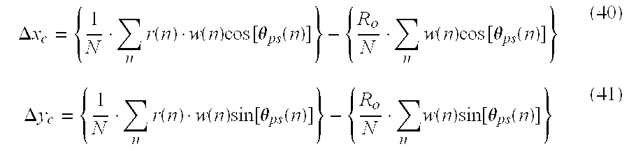
Consider a linear DMNPA that has gain offsets along the coordinate axes that are denoted by Δxc and Δyc. The trajectory of ydet is represented in polar form, wherein an instantaneous radius r is equal to γdet. A phase of the trajectory of γdet is not equal to a phase of the probing signal except when the gain offsets are zero. The phase difference, denoted by δθ, is assumed to be small.
Estimation of Δxc and Δyc involves minimizing the variance of r=γdet. For the case of a sampled signal, the following cost function is minimized: J = n w ( n ) · { [ x 2 ( n ) + y 2 ( n ) ] 0.5 - R o } 2 ( 35 )
Figure US06566948-20030520-M00009
wherein n is a sample index (sample obtained at time t=nT), w(n) is a weight assigned to sample n, r(n)=γdet(n), Ro=E{γdet}, and x ( n ) = r ( n ) · cos [ θ ps ( n ) + δ θ ] - Δ x c ( 36 ) y ( n ) = r ( n ) · sin [ θ ps ( n ) + δ θ ] - Δ y c ( 37 ) θ ps ( n ) = n · 2 π N ( 38 ) sin ( δ θ ) = 1 r ( n ) · { Δ x c · sin [ θ ps ( n ) ] + Δ y c · cos [ θ ps ( n ) ] } ( 39 )
Figure US06566948-20030520-M00010
If it is assumed that δθ is small (i.e., Δxc and Δyc are approximately zero), Δ x c = { 1 N · n r ( n ) · w ( n ) cos [ θ ps ( n ) ] } - { R o N · n w ( n ) cos [ θ ps ( n ) ] } ( 40 ) Δ y c = { 1 N · n r ( n ) · w ( n ) sin [ θ ps ( n ) ] } - { R o N · n w ( n ) sin [ θ ps ( n ) ] } ( 41 )
Figure US06566948-20030520-M00011
It is possible to relate EQ (40) and EQ (41) to the first error measurement: Γ θ = 1 N · n γ det · w ( n ) · - j θ ps ( n ) [ Δ x c - j · Δ y c ] + Γ bias ( 42 )
Figure US06566948-20030520-M00012
where Γ bias = R o N · n w ( n ) · - j θ ps ( n ) ( 43 )
Figure US06566948-20030520-M00013
If Γbias is zero, the gain offsets can be computed without knowledge of Ro.
There are many probing signals that have Γbias=0. One such set of signals is a sine wave whose frequency is altered, even reversed, every 2π rotations around the trajectory. That is, frequency changes or reversals are permitted at a single location on the trajectory.
EQ (43) only requires that the weighted average of the sample points be zero. That is, between samples, the probing signal is not constrained. In general, however, it is preferable to keep the detector error signal γdet constant both at and between sample points in order to avoid stimulating any memory effects within the response of the diode 212. An alternative, and more general, approach for estimating the gain offsets is to estimate and subtract Γbias from the first error measurement, Γθ. EQ (43) dictates that an estimate of Ro be made. With an estimate of Ro, direction reversals are not restricted to a single location on the trajectory. As a result, even a partial trajectory (i.e., an arc) can be used as a probing signal.
Although preferred embodiment(s) of the present invention have been illustrated in the accompanying Drawings and described in the foregoing Description, it will be understood that the present invention is not limited to the embodiment(s) disclosed, but is capable of numerous rearrangements, modifications, and substitutions without departing from the scope of the present invention as set forth and defined by the following claims.

Claims (29)

I claim:
1. A method of reducing non-linearities of a circuit, the method comprising:
providing an input signal, wherein the input signal comprises a constant component and a time-varying component,
pre-distorting the input signal;
inputting the pre-distorted input signal to the circuit;
obtaining an output signal from the circuit;
subtracting a carrier signal from the output signal, thereby yielding an error signal;
determining an envelope of the error signal;
demodulating the envelope of the error signal using a demodulating signal related to the input signal;
adjusting parameters of the pre-distorted input signal with reference to the demodulated converted error signal, thereby causing an amplitude of the envelope of the error signal to approach a constant value.
2. The method of claim 1, wherein the step of demodulating comprises performing a digital Fourier transform (DFT) on the envelope of the error signal.
3. The method of claim 1, wherein the step of determining the envelope of the error signal is performed by a diode.
4. The method of claim 2, wherein the envelope of the error signal comprises:
a constant component;
a fundamental tone; and
a second harmonic tone.
5. The method of claim 1, wherein the step of adjusting comprises varying a phase of the constant component of the pre-distorted input signal.
6. The method of claim 1, wherein the step of adjusting comprises using a Kalman filter to estimate nonlinear and IQ error parameters based at least in part on a set of second harmonic tone measurements at a plurality of pre-distorted signal phase shifts.
7. The method of claim 4, wherein the DFT at the fundamental tone yields a complex value approximately proportional to a gain imbalance between the output signal and the carrier signal.
8. The method of claim 4, wherein the DFT at the first harmonic tone is used to balance gain between the output signal and the carrier signal.
9. The method of claim 1, wherein the pre-distorted input signal excites at least one non-linear mode of the signal-generation circuit.
10. The method of claim 1, wherein the step of adjusting comprises causing the error signal to have substantially no time-varying component.
11. The method of claim 1, further comprising low-pass filtering the demodulated envelope of the error signal prior to the step of converting.
12. The method of claim 1, wherein the constant value is zero.
13. A system for reducing non-linearities comprising:
an input-signal-generation circuit adapted to generate an input signal having a constant component and a time-varying component;
a carrier-signal-generation circuit adapted to generate a carrier signal;
a signal-generation circuit comprising:
an input connected to the input-signal-generation circuit and adapted to receive the input signal;
a modulator connected to the carrier-signal-generation circuit and adapted to modulate the input signal with the carrier signal;
an amplifier connected to the modulator and adapted to amplify the modulated input signal; and
an output connected to the amplifier and adapted to output the modulated amplified input signal;
a pre-distorter adapted to adjust signal parameters and connected to the signal-generation circuit;
a measurement circuit connected to the carrier-signal-generation circuit and to the output and adapted to yield an envelope of an error signal, the envelope comprising a function of an imbalance of the measurement circuit; and
wherein pre-distorter parameter adjustments cause an amplitude of the envelope of the error signal to approach a constant value, thereby reducing non-linearities of the signal-generation circuit.
14. The system of claim 13, wherein the measurement circuit comprises a diode.
15. The system of claim 14, wherein the diode yields the envelope of the error signal.
16. The system of claim 13, wherein the carrier signal and the output signal are aligned as to gain and at least one of phase and time.
17. The system of claim 13, wherein the measurement circuit comprises a demodulation element, the demodulation element being adapted to demodulate the envelope of the error signal using a signal related to the input signal.
18. The system of claim 13, wherein the measurement circuit comprises a low-pass filter adapted to low-pass filter the envelope of the error signal following demodulation of the envelope of the error signal.
19. The system of claim 18, wherein the low-pass filter is implemented via a digital Fourier transform (DFT).
20. The system of claim 17, wherein the demodulation is performed via a digital Fourier transform (DFT).
21. The system of claim 20, wherein the envelope of the error signal comprises:
a constant component;
a fundamental tone; and
a second harmonic tone.
22. The system of claim 21, wherein the DFT at the second harmonic tone yields a complex value approximately proportional to deformations by the signal-generation circuit of the input signal.
23. The system of claim 21, wherein the DFT at the first harmonic tone is used to balance the measurement circuit.
24. The system of claim 21, wherein the DFT at the second harmonic tone is used to estimate non-linear-mode-producing third-order intermodulation distortion and in-phase-quadrature (IQ) errors.
25. The system of claim 13, wherein the pre-distorter parameter adjustments comprise varying a phase of the constant component of the pre-distorted input signal.
26. The system of claim 13, wherein the pre-distorter parameter adjustments comprise use of a Kalman filter to estimate nonlinear and IQ error parameters based at least in part on a set of second harmonic tone measurements at a plurality of pre-distorted signal phase shifts.
27. The system of claim 13, wherein the pre-distorted input signal exites at least one non-linear mode of the signal-generation circuit.
28. The system of claim 13, wherein the pre-distorter parameter adjustments cause the error signal to have substantially no time-varying component.
29. The system of claim 13, wherein the constant value is zero.
US10/084,702 2002-02-26 2002-02-26 Method and system for reducing non-linearities Expired - Lifetime US6566948B1 (en)

Priority Applications (3)

Application Number Priority Date Filing Date Title
US10/084,702 US6566948B1 (en) 2002-02-26 2002-02-26 Method and system for reducing non-linearities
EP02023149A EP1345319A3 (en) 2002-02-26 2002-10-15 Method and system for reducing non-linearities
JP2003046999A JP2003273753A (en) 2002-02-26 2003-02-25 Method and system for reducing nonlinearity

Applications Claiming Priority (1)

Application Number Priority Date Filing Date Title
US10/084,702 US6566948B1 (en) 2002-02-26 2002-02-26 Method and system for reducing non-linearities

Publications (1)

Publication Number Publication Date
US6566948B1 true US6566948B1 (en) 2003-05-20

Family

ID=22186678

Family Applications (1)

Application Number Title Priority Date Filing Date
US10/084,702 Expired - Lifetime US6566948B1 (en) 2002-02-26 2002-02-26 Method and system for reducing non-linearities

Country Status (3)

Country Link
US (1) US6566948B1 (en)
EP (1) EP1345319A3 (en)
JP (1) JP2003273753A (en)

Cited By (20)

* Cited by examiner, † Cited by third party
Publication number Priority date Publication date Assignee Title
EP1528779A1 (en) * 2003-10-29 2005-05-04 Nuovotel Properties A.V.V. System and method for frequency modulation in a modem
US20070222513A1 (en) * 2006-03-09 2007-09-27 Kossor Michael G Apparatus and method for processing of amplifier linearization signals
US20090243727A1 (en) * 2008-03-31 2009-10-01 Bockelman David E Compensating for non-linear capacitance effects in a power amplifier
WO2009126386A1 (en) * 2008-04-10 2009-10-15 Javelin Semiconductor, Inc. Providing pre-distortion to an input signal
US20100085119A1 (en) * 2008-03-31 2010-04-08 Anil Samavedam Generating A Process And Temperature Tracking Bias Voltage
WO2010136114A1 (en) * 2009-05-29 2010-12-02 University College Dublin - National University Of Ireland, Dublin Digital predistorter for rf power amplifiers
US20110074509A1 (en) * 2008-03-31 2011-03-31 Anil Samavedam Non-linear capacitance compensation
US20110121897A1 (en) * 2009-11-25 2011-05-26 Powerwave Technologies, Inc. Measurement and correction of residual nonlinearities in a digitally predistorted power amplifier
EP2575310A1 (en) * 2011-02-25 2013-04-03 Huawei Technologies Co., Ltd. Method and device for digital baseband predistortion
US20130307618A1 (en) * 2012-05-15 2013-11-21 Kiomars Anvari Linearizing a power amplifier
US20140294120A1 (en) * 2013-03-28 2014-10-02 Texas Intsruments Incorporated Dual loop digital predistortion for power amplifiers
US20150010107A1 (en) * 2008-08-11 2015-01-08 Lg Electronics Inc. Method and apparatus for information transmission in a radio communication system
US8964686B2 (en) 2009-02-11 2015-02-24 Lg Electronics Inc. Operation of terminal for multi-antenna transmission
US9031004B2 (en) 2008-11-14 2015-05-12 Lg Electronics Inc. Method and apparatus for information transmission in wireless communication system
US9191931B2 (en) 2008-08-11 2015-11-17 Lg Electronics Inc. Method and apparatus for the transmission of a control signal in a radio communication system
EP2005579A4 (en) * 2006-04-10 2017-02-22 Telefonaktiebolaget LM Ericsson (publ) A method and apparatus for reducing frequency memory effects in rf power amplifiers
US9629152B2 (en) 2008-08-11 2017-04-18 Lg Electronics Inc. Method and apparatus of transmitting information in wireless communication system
US9698953B2 (en) 2008-11-14 2017-07-04 Lg Electronics Inc. Method and apparatus for signal transmission in wireless communication system
US9819412B1 (en) * 2016-05-04 2017-11-14 Inphi Corporation Transmitter gain imbalance and skew optimization for coherent transmitters
US9998216B2 (en) * 2016-05-09 2018-06-12 Fujitsu Limited Skew measurement in an optical coherent transponder

Families Citing this family (1)

* Cited by examiner, † Cited by third party
Publication number Priority date Publication date Assignee Title
EP2378658B1 (en) * 2006-06-27 2013-03-20 Telefonaktiebolaget L M Ericsson (publ) Switched mode power amplification

Citations (5)

* Cited by examiner, † Cited by third party
Publication number Priority date Publication date Assignee Title
US5049832A (en) 1990-04-20 1991-09-17 Simon Fraser University Amplifier linearization by adaptive predistortion
US5420536A (en) 1993-03-16 1995-05-30 Victoria University Of Technology Linearized power amplifier
US5650758A (en) 1995-11-28 1997-07-22 Radio Frequency Systems, Inc. Pipelined digital predistorter for a wideband amplifier
US5742201A (en) 1996-01-30 1998-04-21 Spectrian Polar envelope correction mechanism for enhancing linearity of RF/microwave power amplifier
US20010016354A1 (en) * 1999-06-22 2001-08-23 Angel Cebolla Ramirez Regulated expression of cloned genes using a cascade genetic circuit

Family Cites Families (4)

* Cited by examiner, † Cited by third party
Publication number Priority date Publication date Assignee Title
JPH1022844A (en) * 1996-07-05 1998-01-23 Fujitsu Ltd Nonlinear distortion detection circuit and nonlinear distortion compensation circuit for transmitter
US6232835B1 (en) * 1998-02-13 2001-05-15 Nortel Networks Limited System and method of linearizing the gain error of a power amplifier
US6236837B1 (en) * 1998-07-30 2001-05-22 Motorola, Inc. Polynomial Predistortion linearizing device, method, phone and base station
ATE522023T1 (en) * 2000-01-07 2011-09-15 Powerwave Technologies Inc CARRIER SUPPRESSION MECHANISM FOR A SAMPLING DETECTOR FOR MEASURING AND CORRECTING THE DISTORTION OF THE RF POWER AMPLIFIER

Patent Citations (5)

* Cited by examiner, † Cited by third party
Publication number Priority date Publication date Assignee Title
US5049832A (en) 1990-04-20 1991-09-17 Simon Fraser University Amplifier linearization by adaptive predistortion
US5420536A (en) 1993-03-16 1995-05-30 Victoria University Of Technology Linearized power amplifier
US5650758A (en) 1995-11-28 1997-07-22 Radio Frequency Systems, Inc. Pipelined digital predistorter for a wideband amplifier
US5742201A (en) 1996-01-30 1998-04-21 Spectrian Polar envelope correction mechanism for enhancing linearity of RF/microwave power amplifier
US20010016354A1 (en) * 1999-06-22 2001-08-23 Angel Cebolla Ramirez Regulated expression of cloned genes using a cascade genetic circuit

Non-Patent Citations (1)

* Cited by examiner, † Cited by third party
Title
Martin Weiss, "Check Amplifier Dynamic Behavior With True Test Signals", Microwaves & RF, Dec. 2000, pp. 47-54.

Cited By (42)

* Cited by examiner, † Cited by third party
Publication number Priority date Publication date Assignee Title
WO2005050938A1 (en) * 2003-10-29 2005-06-02 Nuovotel Properties A.V.V. System and method for frequency modulation in a modem
EP1528779A1 (en) * 2003-10-29 2005-05-04 Nuovotel Properties A.V.V. System and method for frequency modulation in a modem
US20070222513A1 (en) * 2006-03-09 2007-09-27 Kossor Michael G Apparatus and method for processing of amplifier linearization signals
US7856105B2 (en) 2006-03-09 2010-12-21 Andrew Llc Apparatus and method for processing of amplifier linearization signals
EP2005579A4 (en) * 2006-04-10 2017-02-22 Telefonaktiebolaget LM Ericsson (publ) A method and apparatus for reducing frequency memory effects in rf power amplifiers
US8219049B2 (en) 2008-03-31 2012-07-10 Javelin Semiconductor, Inc. Generating a process and temperature tracking bias voltage
US20100085119A1 (en) * 2008-03-31 2010-04-08 Anil Samavedam Generating A Process And Temperature Tracking Bias Voltage
US20110074509A1 (en) * 2008-03-31 2011-03-31 Anil Samavedam Non-linear capacitance compensation
US20090243727A1 (en) * 2008-03-31 2009-10-01 Bockelman David E Compensating for non-linear capacitance effects in a power amplifier
US8787850B2 (en) * 2008-03-31 2014-07-22 Avago Technologies General Ip (Singapore) Pte. Ltd. Compensating for non-linear capacitance effects in a power amplifier
US8344808B2 (en) 2008-03-31 2013-01-01 Javelin Semiconductor, Inc. Non-linear capacitance compensation
US9065405B2 (en) 2008-03-31 2015-06-23 Avago Technologies General Ip (Singapore) Pte. Ltd. Compensating for non-linear capacitance effects in a power amplifier
US8907727B2 (en) 2008-03-31 2014-12-09 Avago Technologies General Ip (Singapore) Pte. Ltd. Non-linear capacitance compensation
US20090256631A1 (en) * 2008-04-10 2009-10-15 Bockelman David E Providing pre-distortion to an input signal
WO2009126386A1 (en) * 2008-04-10 2009-10-15 Javelin Semiconductor, Inc. Providing pre-distortion to an input signal
US7872528B2 (en) 2008-04-10 2011-01-18 Javelin Semiconductor, Inc. Providing pre-distortion to an input signal
US9191931B2 (en) 2008-08-11 2015-11-17 Lg Electronics Inc. Method and apparatus for the transmission of a control signal in a radio communication system
US9094156B2 (en) 2008-08-11 2015-07-28 Lg Electronics Inc. Method and apparatus for information transmission in a radio communication system
US9629152B2 (en) 2008-08-11 2017-04-18 Lg Electronics Inc. Method and apparatus of transmitting information in wireless communication system
US9537621B2 (en) 2008-08-11 2017-01-03 Lg Electronics Inc. Method and apparatus for information transmission in a radio communication system
US9197383B2 (en) 2008-08-11 2015-11-24 Lg Electronics Inc. Method and apparatus for information transmission in a radio communication system
US8989304B2 (en) * 2008-08-11 2015-03-24 Lg Electronics Inc. Method and apparatus for information transmission in a radio communication system
US20150010107A1 (en) * 2008-08-11 2015-01-08 Lg Electronics Inc. Method and apparatus for information transmission in a radio communication system
US9949242B2 (en) 2008-11-14 2018-04-17 Lg Electronics Inc. Method and apparatus for information transmission in wireless communication system
US9698953B2 (en) 2008-11-14 2017-07-04 Lg Electronics Inc. Method and apparatus for signal transmission in wireless communication system
US9031004B2 (en) 2008-11-14 2015-05-12 Lg Electronics Inc. Method and apparatus for information transmission in wireless communication system
US9674824B2 (en) 2008-11-14 2017-06-06 Lg Electronics Inc. Method and apparatus for information transmission in wireless communication system
US9288806B2 (en) 2008-11-14 2016-03-15 Lg Electronics Inc. Method and apparatus for information transmission in wireless communication system
US9214997B2 (en) 2009-02-11 2015-12-15 Lg Electronics Inc. Operation of terminal for multi-antenna transmission
US8964686B2 (en) 2009-02-11 2015-02-24 Lg Electronics Inc. Operation of terminal for multi-antenna transmission
WO2010136114A1 (en) * 2009-05-29 2010-12-02 University College Dublin - National University Of Ireland, Dublin Digital predistorter for rf power amplifiers
US20110121897A1 (en) * 2009-11-25 2011-05-26 Powerwave Technologies, Inc. Measurement and correction of residual nonlinearities in a digitally predistorted power amplifier
US8354884B2 (en) 2009-11-25 2013-01-15 Powerwave Technologies, Inc. Measurement and correction of residual nonlinearities in a digitally predistorted power amplifier
EP2575310A4 (en) * 2011-02-25 2013-10-16 Huawei Tech Co Ltd Method and device for digital baseband predistortion
EP2575310A1 (en) * 2011-02-25 2013-04-03 Huawei Technologies Co., Ltd. Method and device for digital baseband predistortion
US8855233B2 (en) 2011-02-25 2014-10-07 Huawei Technologies Co., Ltd. Method and apparatus for implementing digital baseband predistortion
US20130307618A1 (en) * 2012-05-15 2013-11-21 Kiomars Anvari Linearizing a power amplifier
US8779851B2 (en) * 2012-05-15 2014-07-15 Integrated Device Technology, Inc. Linearizing a power amplifier
US20140294120A1 (en) * 2013-03-28 2014-10-02 Texas Intsruments Incorporated Dual loop digital predistortion for power amplifiers
US9001928B2 (en) * 2013-03-28 2015-04-07 Texas Instruments Incorporated Transmitter first/second digital predistortion and first/second adaption circuitry with feedback
US9819412B1 (en) * 2016-05-04 2017-11-14 Inphi Corporation Transmitter gain imbalance and skew optimization for coherent transmitters
US9998216B2 (en) * 2016-05-09 2018-06-12 Fujitsu Limited Skew measurement in an optical coherent transponder

Also Published As

Publication number Publication date
EP1345319A2 (en) 2003-09-17
JP2003273753A (en) 2003-09-26
EP1345319A3 (en) 2005-07-06

Similar Documents

Publication Publication Date Title
US6566948B1 (en) Method and system for reducing non-linearities
US6593812B2 (en) Automatic optimization of linearity for envelope feedback RF amplifier linearization
EP1224733B1 (en) Adaptive linearization of power amplifiers
US6987954B2 (en) Feedback compensation detector for a direct conversion transmitter
US8150335B2 (en) Apparatus and method for adaptive cartesian transmitter linearization and wireless transmitter employing the same
RU2336628C2 (en) Device and method of amplifier pre-distortion and autocalibration
US8442460B2 (en) Method for compensating signal distortions in composite amplifiers
US4878030A (en) Linearizer for microwave amplifier
US7539268B2 (en) Transmission/reception arrangement and method for reducing nonlinearities in output signals from a transmission/reception arrangement
US7145962B2 (en) Predistortion digital linearizer and gain controlling method thereof
US8326239B1 (en) Power amplifier linearization using digital predistortion
US7415250B2 (en) Distortion compensating amplifier
US20100074367A1 (en) Adaptive combiner error calibration algorithms in all-digital outphasing transmitter
US20040166813A1 (en) Cartesian loop systems with digital processing
JP6340207B2 (en) Nonlinear distortion detector and distortion compensation power amplifier
US7120561B2 (en) Phase-error based signal alignment
JP3144649B2 (en) Distortion compensated quadrature modulator
JPH0531326B2 (en)
US8538349B2 (en) Method and device for pre-distorting an exciter and predistortion exciter
KR100417413B1 (en) Digital linear apparatus
Lohtia et al. Adaptive digital linearization of RF power amplifiers
Madhuwantha et al. Novel Calibration Technique for Wideband Transmitters using Constellation Mapping
CN112511175A (en) IQ mismatch estimation circuit, zero IF transmitter and method thereof
JP2006148781A (en) High frequency power amplifying device and its distortion compensation method
JP2003110370A (en) Distortion compensating device

Legal Events

Date Code Title Description
AS Assignment

Owner name: AGILENT TECHNOLOGIES, INC., COLORADO

Free format text: ASSIGNMENT OF ASSIGNORS INTEREST;ASSIGNOR:BRAITHWAITE, RICHARD NEIL;REEL/FRAME:012808/0579

Effective date: 20020401

STCF Information on status: patent grant

Free format text: PATENTED CASE

FPAY Fee payment

Year of fee payment: 4

FPAY Fee payment

Year of fee payment: 8

AS Assignment

Owner name: KEYSIGHT TECHNOLOGIES, INC., CALIFORNIA

Free format text: ASSIGNMENT OF ASSIGNORS INTEREST;ASSIGNOR:AGILENT TECHNOLOGIES, INC.;REEL/FRAME:033746/0714

Effective date: 20140801

FPAY Fee payment

Year of fee payment: 12