EP1344849A1 - ELECTROLYTIC COPPER PLATING METHOD, ELECTROLYTIC COPPER PLATING−USE PHOSPHORUS−CONTAINING COPPER ANODE AND SEMICONDUCTOR WAFER WITH LITTLE PARTICLES DEPOSITION PLATED BY USING THEM - Google Patents
ELECTROLYTIC COPPER PLATING METHOD, ELECTROLYTIC COPPER PLATING−USE PHOSPHORUS−CONTAINING COPPER ANODE AND SEMICONDUCTOR WAFER WITH LITTLE PARTICLES DEPOSITION PLATED BY USING THEM Download PDFInfo
- Publication number
- EP1344849A1 EP1344849A1 EP02745950A EP02745950A EP1344849A1 EP 1344849 A1 EP1344849 A1 EP 1344849A1 EP 02745950 A EP02745950 A EP 02745950A EP 02745950 A EP02745950 A EP 02745950A EP 1344849 A1 EP1344849 A1 EP 1344849A1
- Authority
- EP
- European Patent Office
- Prior art keywords
- anode
- copper
- phosphorous
- electrolytic copper
- copper plating
- Prior art date
- Legal status (The legal status is an assumption and is not a legal conclusion. Google has not performed a legal analysis and makes no representation as to the accuracy of the status listed.)
- Granted
Links
Images
Classifications
-
- C—CHEMISTRY; METALLURGY
- C25—ELECTROLYTIC OR ELECTROPHORETIC PROCESSES; APPARATUS THEREFOR
- C25D—PROCESSES FOR THE ELECTROLYTIC OR ELECTROPHORETIC PRODUCTION OF COATINGS; ELECTROFORMING; APPARATUS THEREFOR
- C25D7/00—Electroplating characterised by the article coated
- C25D7/12—Semiconductors
-
- C—CHEMISTRY; METALLURGY
- C25—ELECTROLYTIC OR ELECTROPHORETIC PROCESSES; APPARATUS THEREFOR
- C25D—PROCESSES FOR THE ELECTROLYTIC OR ELECTROPHORETIC PRODUCTION OF COATINGS; ELECTROFORMING; APPARATUS THEREFOR
- C25D17/00—Constructional parts, or assemblies thereof, of cells for electrolytic coating
- C25D17/10—Electrodes, e.g. composition, counter electrode
Definitions
- the present invention pertains to an electrolytic copper plating method and a phosphorous copper anode used in such electrolytic copper plating method capable of suppressing the generation of particles such as sludge produced on the anode side within the plating bath, and in particular capable of preventing the adhesion of particles to a semiconductor wafer, as well as to a semiconductor wafer having low particle adhesion plated with the foregoing method and anode.
- an electrolytic copper plate has been employed for forming copper wiring in a PWB (print wiring board) or the like, in recent years, it is being used for forming copper wiring of semiconductors.
- An electrolytic copper plate has a long history, and it has reached its present form upon accumulating numerous technical advancements. Nevertheless, when employing this electrolytic copper plate for forming copper wiring of semiconductors, a new problem arose which was not found in a PWB.
- phosphorous copper is used as the anode.
- an insoluble anode formed from the likes of platinum, titanium, or iridium oxide is used, the additive within the plating liquid would decompose upon being affected by anodic oxidization, and inferior plating will occur thereby.
- electrolytic copper or oxygen-free copper of a soluble anode a large amount of particles such as sludge is generated from metallic copper or copper oxide caused by the disproportionation reaction of monovalent copper during dissolution, and the object to be plated will become contaminated as a result thereof.
- a black film composed of copper phosphide and copper chloride is formed on the anode surface due to electrolysis, and it is thereby possible to suppress the generation of metallic copper or copper oxide caused by the disproportionation reaction of monovalent copper, and to control the generation of particles.
- a filter cloth referred to as an anode bag is ordinarily used to wrap the anode so as to prevent particles from reaching the plating liquid.
- the present invention aims to provide an electrolytic copper plating method and a phosphorous copper anode used in such electrolytic copper plating method capable of suppressing the generation of particles such as sludge produced on the anode side within the plating bath, and in particular capable of preventing the adhesion of particles to a semiconductor wafer, as well as to a semiconductor wafer having low particle adhesion plated with the foregoing method and anode.
- a semiconductor wafer and the like having low particle adhesion can be manufactured stably by improving the electrode material, and suppressing the generation or particles in the anode.
- the present invention provides:
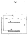
- Fig. 1 is a conceptual diagram of a device used in the electrolytic copper plating method of a semiconductor according to the present invention.
- Fig. 1 is a diagram illustrating an example of the device employed in the electrolytic copper plating method of a semiconductor wafer.
- This copper plating device comprises a tank 1 having copper sulfate plating liquid 2.
- An anode 4 composed of a phosphorous copper anode as the anode is used, and, as the cathode, for example, a semiconductor wafer is used as the object of plating.
- a black film composed of copper phosphide and copper chloride is formed on the surface, and this yields the function of suppressing the generation of particles such as sludge composed of metallic copper or copper oxide caused by the disproportionation reaction of monovalent copper during the dissolution of the anode.
- the generation speed of the black film is strongly influenced by the current density of the anode, crystal grain size, phosphorous content, and so on, and, higher the current density, smaller the crystal grain size, and higher the phosphorous content, the foregoing generation speed becomes faster, and, as a result, it has become evident that the black film tends to become thicker as a result thereof.
- the present invention proposes a phosphorous copper anode representing the foregoing optimum values.
- the phosphorous copper anode of the present invention makes the crystal grain size of the phosphorous copper anode 10 to 1500 ⁇ m, preferably 20 to 700 ⁇ m, when the anode current density during electrolysis is 3A/dm 2 or more, and makes the grain size of the phosphorous copper anode 5 to 1500 ⁇ m, preferably 10 to 700 ⁇ m, when the anode current density during electrolysis is less than 3A/dm 2 .
- the phosphorous content of the phosphorous copper anode be set between 50 and 2000wtppm as the appropriate composition ratio for suppressing the generation of particles.
- a black film layer with a thickness of 1000 ⁇ m or less and having copper phosphide or copper chloride as its principle component may be formed on the phosphorous copper anode surface upon electrolytic copper plating.
- the anode current density upon performing electrolytic copper plating is usually 1 to 5A/dm 2
- the subject is a new anode in which the black film has not been formed thereon
- electrolysis is performed at a high current density from the initial stages of such electrolysis, a black film having favorable adhesiveness cannot be obtained.
- the generation of sludge or the like can be reduced significantly, and it is further possible to prevent particles from reaching the semiconductor wafer and causing inferior plating upon such particles adhering to the semiconductor wafer.
- the electrolytic plate employing the phosphorous copper anode of the present invention is particularly effective in the plating of a semiconductor wafer, but is also effective for copper plating in other sectors where fine lines are on the rise, and may be employed as an effective method for reducing the inferior ratio of plating caused by particles.
- the phosphorous copper anode of the present invention yields an effect of suppressing the irruption of particles such as sludge composed of metallic copper or copper oxide, and significantly reducing the contamination of the object to be plated, but does not cause the decomposition of additives within the plating liquid or inferior plating resulting therefrom which occurred during the use of insoluble anodes in the past.
- the plating liquid As the plating liquid, an appropriate amount of copper sulfate: 10 to 70g/L (Cu), sulfuric acid: 10 to 300g/L, chlorine ion 20 to 100mg/L, additive: (CC-1220: 1mL/L or the like manufactured by Nikko Metal Plating) may be used. Moreover, it is desirable that the purity of the copper sulfate be 99.9% or higher.
- the plating temperature is 15 to 35°C
- cathode current density is 0.5 to 5.5A/dm 2
- anode current density is 0.5 to 5.5A/dm 2
- plating time is 0.5 to 100hr.
- phosphorous copper having a phosphorous content of 300 to 600wtppm was used as the anode, and a semiconductor was used as the cathode.
- the crystal grain size of these phosphorous copper anodes was 10 to 200 ⁇ m.
- copper sulfate 20 to 55g/L (Cu)
- sulfuric acid 10 to 200g/L
- additive [brightening agent, surface active agent] (Product Name CC-1220: manufactured by Nikko Metal Plating): 1mL/L were used.
- the purity of the copper sulfate within the plating liquid was 99.99%.
- the plating conditions were plating temperature 30°C, cathode current density 1.0 to 5.0A/dm 2 , anode current density 1.0 to 5.0A/dm 2 , and plating time 19 to 96hr.
- the foregoing conditions are shown in Table 1.
- the plating liquid was filtered with a filter of 0.2 ⁇ m, and the weight of the filtrate was measured thereby.
- the object to be plated was exchanged, plating was conducted for 3 minutes, and the existence of bums, clouding, swelling, abnormal deposition, foreign material adhesion and so on were observed visually.
- the amount of particles was less than 1mg in Examples 1 to 4, and the plate appearance was favorable.
- phosphorous copper having a phosphorous content of 500wtppm was used as the anode, and a semiconductor was used as the cathode.
- the crystal grain size of these phosphorous copper anodes was 200 ⁇ m.
- copper sulfate 55g/L (Cu)
- sulfuric acid 10g/L
- additive [brightening agent, surface active agent] (Product Name CC-1220: manufactured by Nikko Metal Plating): 1mL/L were used.
- the purity of the copper sulfate within the plating liquid was 99.99%.
- the plating conditions were plating temperature 30°C, cathode current density 1.0 to 5.0A/dm 2 , anode current density 1.0 to 5.0A/dm 2 , and plating time 24 to 48hr.
- Examples 5 to 8 in particular, illustrated are examples in which minute crystal layers having a crystal grain size of 5 ⁇ m and 10 ⁇ m were previously formed on the anode surface at a thickness of 100 ⁇ m, and a black film was also formed thereon at a thickness of 100 ⁇ m and 200 ⁇ m.
- the amount of particles was less than 1mg in Examples 5 to 8, and the plate appearance was favorable.
- a prescribed plate was acquired in a short period of time with a relatively low current density. This is considered to be because minute crystal layers having a crystal grain size of 5 ⁇ m and 10 ⁇ m were previously formed on the anode surface at a thickness of 100 ⁇ m, and a black film was also formed thereon at a thickness of 100 ⁇ m and 200 ⁇ m.
- phosphorous copper having a phosphorous content of 500wtppm was used as the anode, and a semiconductor was used as the cathode.
- the crystal grain size of these phosphorous copper anodes was 3 ⁇ m and 2000 ⁇ m, which are both outside the scope of the present invention.
- copper sulfate 55g/L (Cu)
- sulfuric acid 10g/L
- additive [brightening agent, surface active agent] (Product Name CC-1220: manufactured by Nikko Metal Plating): 1mL/L were used.
- the purity of the copper sulfate within the plating liquid was 99.99%.
- the plating conditions were plating temperature 30°C, cathode current density 1.0 to 5.0A/dm 2 , anode current density 1.0 to 5.0A/dm 2 , and plating time 19 to 96hr.
- the foregoing conditions are shown in Table 3.
- the present invention yields a superior effect in that it is capable of suppressing the generation of particles such as sludge produced on the anode side within the plating bath, and capable of significantly preventing the adhesion of particles to a semiconductor wafer.
Landscapes
- Chemical & Material Sciences (AREA)
- Engineering & Computer Science (AREA)
- Chemical Kinetics & Catalysis (AREA)
- Electrochemistry (AREA)
- Materials Engineering (AREA)
- Metallurgy (AREA)
- Organic Chemistry (AREA)
- Electroplating Methods And Accessories (AREA)
- Electrodes Of Semiconductors (AREA)
- Electroplating And Plating Baths Therefor (AREA)
Abstract
Description


Claims (14)
- An electrolytic copper plating method characterized in employing phosphorous copper as the anode upon performing electrolytic copper plating, and performing electrolytic copper plating upon making the crystal grain size of said phosphorous copper anode 10 to 1500 µ m when the anode current density during electrolysis is 3A/dm2 or more, and making the grain size of said phosphorous copper anode 5 to 1500 µ m when the anode current density during electrolysis is less than 3A/dm2.
- An electrolytic copper plating method characterized in employing phosphorous copper as the anode upon performing electrolytic copper plating, and performing electrolytic copper plating upon making the crystal grain size of said phosphorous copper anode 20 to 700 µ m when the anode current density during electrolysis is 3A/dm2 or more, and making the grain size of said phosphorous copper anode 10 to 700 µ m when the anode current density during electrolysis is less than 3A/dm2.
- An electrolytic copper plating method according to claim 1 or claim 2, wherein the phosphorous content of the phosphorous copper anode is 50 to 2000wtppm.
- An electrolytic copper plating method characterized in employing phosphorous copper as the anode upon performing electrolytic copper plating, and forming in advance a minute crystal layer having a crystal grain size of 1 to 100 µ m on the surface of the phosphorous copper anode.
- An electrolytic copper plating method according to each of claims 1 to 3, characterized in employing phosphorous copper as the anode upon performing electrolytic copper plating, and forming in advance a minute crystal layer having a crystal grain size of 1 to 100 µ m on the surface of the phosphorous copper anode.
- An electrolytic copper plating method according to each of claims 1 to 3 and claim 5, characterized in that the phosphorous copper anode surface has a black film with a thickness of 1000 µ m or less and having copper phosphide or copper chloride as its principle component.
- A phosphorous copper anode for electrolytic copper plating characterized in that phosphorous copper is used as the anode for performing electrolytic copper plating, and the crystal grain size of said phosphorous copper anode is 5 to 1500 µ m.
- A phosphorous copper anode for electrolytic copper plating characterized in that phosphorous copper is used as the anode for performing electrolytic copper plating, and the crystal grain size of said phosphorous copper anode is 10 to 700 µ m.
- A phosphorous copper anode for electrolytic copper plating according to claim 7 or claim 8, wherein the phosphorous content of the phosphorous copper anode is 50 to 2000wtppm.
- A phosphorous copper anode for electrolytic copper plating characterized in that phosphorous copper is used as the anode for performing electrolytic copper plating, and a minute crystal layer having a crystal grain size of 1 to 100 µ m is formed in advance on the surface of the phosphorous copper anode.
- A phosphorous copper anode for electrolytic copper plating according to each of claims 7 to 9, characterized in that phosphorous copper is used as the anode for performing electrolytic copper plating, and a minute crystal layer having a crystal grain size of 1 to 100 µm is formed in advance on the surface of the phosphorous copper anode.
- A phosphorous copper anode for electrolytic copper plating according to each of claims 7 to 9 and claim 11, characterized in that the phosphorous copper anode surface has a black film with a thickness of 1000 µ m or less and having copper phosphide or copper chloride as its principle component.
- An electrolytic copper plating method and a phosphorous copper anode for electrolytic copper plating according to each of claims 1 to 12, characterized in that the electrolytic copper plating is to be performed on a semiconductor wafer.
- A semiconductor wafer having low particle adhesion plated with the electrolytic copper plating method and the phosphorous copper anode for electrolytic copper plating according to each of claims 1 to 13.
Priority Applications (1)
| Application Number | Priority Date | Filing Date | Title |
|---|---|---|---|
| EP08168461A EP2019154A1 (en) | 2001-10-22 | 2002-07-11 | Electrolytic copper plating method, phosphorous copper anode for electrolytic copper plating method, and semiconductor wafer having low particle adhesion plated with said method and anode |
Applications Claiming Priority (3)
| Application Number | Priority Date | Filing Date | Title |
|---|---|---|---|
| JP2001323265A JP4076751B2 (en) | 2001-10-22 | 2001-10-22 | Electro-copper plating method, phosphor-containing copper anode for electrolytic copper plating, and semiconductor wafer plated with these and having less particle adhesion |
| JP2001323265 | 2001-10-22 | ||
| PCT/JP2002/007038 WO2003035943A1 (en) | 2001-10-22 | 2002-07-11 | Electrolytic copper plating method, electrolytic copper plating-use phosphorus-containing copper anode and semiconductor wafer with little particles deposition plated by using them |
Related Child Applications (2)
| Application Number | Title | Priority Date | Filing Date |
|---|---|---|---|
| EP08168461A Division EP2019154A1 (en) | 2001-10-22 | 2002-07-11 | Electrolytic copper plating method, phosphorous copper anode for electrolytic copper plating method, and semiconductor wafer having low particle adhesion plated with said method and anode |
| EP08168461A Division-Into EP2019154A1 (en) | 2001-10-22 | 2002-07-11 | Electrolytic copper plating method, phosphorous copper anode for electrolytic copper plating method, and semiconductor wafer having low particle adhesion plated with said method and anode |
Publications (3)
| Publication Number | Publication Date |
|---|---|
| EP1344849A1 true EP1344849A1 (en) | 2003-09-17 |
| EP1344849A4 EP1344849A4 (en) | 2007-12-26 |
| EP1344849B1 EP1344849B1 (en) | 2016-12-07 |
Family
ID=19140183
Family Applications (2)
| Application Number | Title | Priority Date | Filing Date |
|---|---|---|---|
| EP08168461A Withdrawn EP2019154A1 (en) | 2001-10-22 | 2002-07-11 | Electrolytic copper plating method, phosphorous copper anode for electrolytic copper plating method, and semiconductor wafer having low particle adhesion plated with said method and anode |
| EP02745950.2A Expired - Lifetime EP1344849B1 (en) | 2001-10-22 | 2002-07-11 | Electrolytic copper plating method, phosphorus copper anode for electrolytic copper plating method, and semiconductor wafer having low particle adhesion plated with said method and anode |
Family Applications Before (1)
| Application Number | Title | Priority Date | Filing Date |
|---|---|---|---|
| EP08168461A Withdrawn EP2019154A1 (en) | 2001-10-22 | 2002-07-11 | Electrolytic copper plating method, phosphorous copper anode for electrolytic copper plating method, and semiconductor wafer having low particle adhesion plated with said method and anode |
Country Status (7)
| Country | Link |
|---|---|
| US (1) | US7138040B2 (en) |
| EP (2) | EP2019154A1 (en) |
| JP (1) | JP4076751B2 (en) |
| KR (1) | KR100577519B1 (en) |
| CN (1) | CN100343423C (en) |
| TW (1) | TW562880B (en) |
| WO (1) | WO2003035943A1 (en) |
Families Citing this family (19)
| Publication number | Priority date | Publication date | Assignee | Title |
|---|---|---|---|---|
| JP3876253B2 (en) * | 2001-08-01 | 2007-01-31 | 日鉱金属株式会社 | Manufacturing method of high purity nickel |
| JP4011336B2 (en) * | 2001-12-07 | 2007-11-21 | 日鉱金属株式会社 | Electro-copper plating method, pure copper anode for electro-copper plating, and semiconductor wafer plated with these with less particle adhesion |
| JP4034095B2 (en) * | 2002-03-18 | 2008-01-16 | 日鉱金属株式会社 | Electro-copper plating method and phosphorous copper anode for electro-copper plating |
| CN1301910C (en) * | 2002-09-05 | 2007-02-28 | 日矿金属株式会社 | High-purity copper sulfate and preparation method thereof |
| US7704368B2 (en) * | 2005-01-25 | 2010-04-27 | Taiwan Semiconductor Manufacturing Co. Ltd. | Method and apparatus for electrochemical plating semiconductor wafers |
| JP2007262456A (en) * | 2006-03-27 | 2007-10-11 | Hitachi Cable Ltd | Copper ball for positive electrode of copper plating, plating apparatus, copper plating method, and printed circuit board manufacturing method |
| EP2213772B1 (en) * | 2007-11-01 | 2016-08-17 | JX Nippon Mining & Metals Corporation | Phosphorus-containing copper anode |
| JP4554662B2 (en) * | 2007-11-21 | 2010-09-29 | 日鉱金属株式会社 | Phosphorus copper anode for electrolytic copper plating and method for producing the same |
| JP5499933B2 (en) * | 2010-01-12 | 2014-05-21 | 三菱マテリアル株式会社 | Phosphorous copper anode for electrolytic copper plating, method for producing the same, and electrolytic copper plating method |
| JP5376168B2 (en) * | 2010-03-30 | 2013-12-25 | 三菱マテリアル株式会社 | High purity copper anode for electrolytic copper plating, manufacturing method thereof, and electrolytic copper plating method |
| JP5668915B2 (en) * | 2010-09-06 | 2015-02-12 | 三菱マテリアル株式会社 | Method for producing phosphorus-containing copper anode material for plating, in which phosphorus component is uniformly dispersed and having a fine uniform crystal structure, and phosphorus-containing copper anode material for plating |
| JP5590328B2 (en) * | 2011-01-14 | 2014-09-17 | 三菱マテリアル株式会社 | Phosphorus-containing copper anode for electrolytic copper plating and electrolytic copper plating method using the same |
| JP5626582B2 (en) * | 2011-01-21 | 2014-11-19 | 三菱マテリアル株式会社 | Phosphorus copper anode for electrolytic copper plating and electrolytic copper plating method using the same |
| JP2014237865A (en) * | 2013-06-06 | 2014-12-18 | 株式会社荏原製作所 | Electrolytic copper plating apparatus |
| JP6619942B2 (en) * | 2015-03-06 | 2019-12-11 | Jx金属株式会社 | Copper anode or phosphorus-containing copper anode used for electrolytic copper plating on semiconductor wafer and method for producing copper anode or phosphorus-containing copper anode |
| CN105586630A (en) * | 2015-12-23 | 2016-05-18 | 南通富士通微电子股份有限公司 | Method for improving quality of black film of copper and phosphorus anode in semiconductor packaging |
| CN107217295A (en) * | 2017-05-27 | 2017-09-29 | 佛山市承安铜业有限公司 | A kind of method for studying phosphorus-copper anode film forming situation |
| JP2017186677A (en) * | 2017-05-29 | 2017-10-12 | 株式会社荏原製作所 | Electrolytic copper plating equipment |
| JP6960363B2 (en) | 2018-03-28 | 2021-11-05 | Jx金属株式会社 | Co-anode, electric Co-plating method using Co-anode and evaluation method of Co-anode |
Family Cites Families (8)
| Publication number | Priority date | Publication date | Assignee | Title |
|---|---|---|---|---|
| JP3833035B2 (en) | 2000-01-07 | 2006-10-11 | 株式会社荏原製作所 | Substrate plating equipment |
| JP4394234B2 (en) | 2000-01-20 | 2010-01-06 | 日鉱金属株式会社 | Copper electroplating solution and copper electroplating method |
| US6503375B1 (en) | 2000-02-11 | 2003-01-07 | Applied Materials, Inc | Electroplating apparatus using a perforated phosphorus doped consumable anode |
| KR20010107766A (en) * | 2000-05-26 | 2001-12-07 | 마에다 시게루 | Substrate processing apparatus and substrate plating apparatus |
| JP3874609B2 (en) | 2000-12-04 | 2007-01-31 | 株式会社荏原製作所 | Plating method |
| US6531039B2 (en) * | 2001-02-21 | 2003-03-11 | Nikko Materials Usa, Inc. | Anode for plating a semiconductor wafer |
| JP4123330B2 (en) * | 2001-03-13 | 2008-07-23 | 三菱マテリアル株式会社 | Phosphorus copper anode for electroplating |
| JP4034095B2 (en) * | 2002-03-18 | 2008-01-16 | 日鉱金属株式会社 | Electro-copper plating method and phosphorous copper anode for electro-copper plating |
-
2001
- 2001-10-22 JP JP2001323265A patent/JP4076751B2/en not_active Expired - Lifetime
-
2002
- 2002-07-11 EP EP08168461A patent/EP2019154A1/en not_active Withdrawn
- 2002-07-11 KR KR1020037008562A patent/KR100577519B1/en not_active Expired - Lifetime
- 2002-07-11 US US10/362,152 patent/US7138040B2/en not_active Expired - Lifetime
- 2002-07-11 EP EP02745950.2A patent/EP1344849B1/en not_active Expired - Lifetime
- 2002-07-11 WO PCT/JP2002/007038 patent/WO2003035943A1/en not_active Ceased
- 2002-07-11 CN CNB028015223A patent/CN100343423C/en not_active Expired - Lifetime
- 2002-10-04 TW TW091122954A patent/TW562880B/en not_active IP Right Cessation
Also Published As
| Publication number | Publication date |
|---|---|
| WO2003035943A1 (en) | 2003-05-01 |
| CN1529774A (en) | 2004-09-15 |
| JP2003129295A (en) | 2003-05-08 |
| KR20030063466A (en) | 2003-07-28 |
| TW562880B (en) | 2003-11-21 |
| EP2019154A1 (en) | 2009-01-28 |
| JP4076751B2 (en) | 2008-04-16 |
| US20040007474A1 (en) | 2004-01-15 |
| US7138040B2 (en) | 2006-11-21 |
| KR100577519B1 (en) | 2006-05-10 |
| EP1344849B1 (en) | 2016-12-07 |
| CN100343423C (en) | 2007-10-17 |
| EP1344849A4 (en) | 2007-12-26 |
Similar Documents
| Publication | Publication Date | Title |
|---|---|---|
| US8252157B2 (en) | Electrolytic copper plating method, phosphorous copper anode for electrolytic copper plating, and semiconductor wafer having low particle adhesion plated with said method and anode | |
| US7138040B2 (en) | Electrolytic copper plating method, phosphorous copper anode for electrolytic plating method, and semiconductor wafer having low particle adhesion plated with said method and anode | |
| US7943033B2 (en) | Electrolytic copper plating method, pure copper anode for electrolytic copper plating, and semiconductor wafer having low particle adhesion plated with said method and anode | |
| EP2213772B1 (en) | Phosphorus-containing copper anode | |
| JP4607165B2 (en) | Electro copper plating method | |
| JP4064121B2 (en) | Electro-copper plating method using phosphorous copper anode | |
| JP4554662B2 (en) | Phosphorus copper anode for electrolytic copper plating and method for producing the same | |
| JP5234844B2 (en) | Electro-copper plating method, phosphor-containing copper anode for electrolytic copper plating, and semiconductor wafer plated with these and having less particle adhesion | |
| JP5179549B2 (en) | Electro copper plating method | |
| JP2003213498A (en) | Anode for electrolytic copper plating, method for producing the anode, method for electrolytic copper plating using the anode, and plated object with less adhesion of particles plated using the same |
Legal Events
| Date | Code | Title | Description |
|---|---|---|---|
| PUAI | Public reference made under article 153(3) epc to a published international application that has entered the european phase |
Free format text: ORIGINAL CODE: 0009012 |
|
| 17P | Request for examination filed |
Effective date: 20030314 |
|
| AK | Designated contracting states |
Kind code of ref document: A1 Designated state(s): AT BE BG CH CY CZ DE DK EE ES FI FR GB GR IE IT LI LU MC NL PT SE SK TR |
|
| AX | Request for extension of the european patent |
Extension state: AL LT LV MK RO SI |
|
| RAP1 | Party data changed (applicant data changed or rights of an application transferred) |
Owner name: NIKKO MATERIALS CO., LTD. |
|
| RAP1 | Party data changed (applicant data changed or rights of an application transferred) |
Owner name: NIPPON MINING & METALS CO., LTD. |
|
| A4 | Supplementary search report drawn up and despatched |
Effective date: 20071122 |
|
| 17Q | First examination report despatched |
Effective date: 20080505 |
|
| RAP1 | Party data changed (applicant data changed or rights of an application transferred) |
Owner name: JX NIPPON MINING & METALS CORPORATION |
|
| GRAP | Despatch of communication of intention to grant a patent |
Free format text: ORIGINAL CODE: EPIDOSNIGR1 |
|
| INTG | Intention to grant announced |
Effective date: 20160721 |
|
| GRAS | Grant fee paid |
Free format text: ORIGINAL CODE: EPIDOSNIGR3 |
|
| GRAA | (expected) grant |
Free format text: ORIGINAL CODE: 0009210 |
|
| AK | Designated contracting states |
Kind code of ref document: B1 Designated state(s): DE FR GB IT |
|
| REG | Reference to a national code |
Ref country code: GB Ref legal event code: FG4D |
|
| REG | Reference to a national code |
Ref country code: DE Ref legal event code: R096 Ref document number: 60248540 Country of ref document: DE |
|
| REG | Reference to a national code |
Ref country code: FR Ref legal event code: PLFP Year of fee payment: 16 |
|
| REG | Reference to a national code |
Ref country code: DE Ref legal event code: R097 Ref document number: 60248540 Country of ref document: DE |
|
| PLBE | No opposition filed within time limit |
Free format text: ORIGINAL CODE: 0009261 |
|
| REG | Reference to a national code |
Ref country code: FR Ref legal event code: CA Effective date: 20170912 |
|
| STAA | Information on the status of an ep patent application or granted ep patent |
Free format text: STATUS: NO OPPOSITION FILED WITHIN TIME LIMIT |
|
| 26N | No opposition filed |
Effective date: 20170908 |
|
| REG | Reference to a national code |
Ref country code: FR Ref legal event code: PLFP Year of fee payment: 17 |
|
| PGFP | Annual fee paid to national office [announced via postgrant information from national office to epo] |
Ref country code: FR Payment date: 20210611 Year of fee payment: 20 Ref country code: IT Payment date: 20210610 Year of fee payment: 20 |
|
| PGFP | Annual fee paid to national office [announced via postgrant information from national office to epo] |
Ref country code: GB Payment date: 20210616 Year of fee payment: 20 |
|
| PGFP | Annual fee paid to national office [announced via postgrant information from national office to epo] |
Ref country code: DE Payment date: 20210616 Year of fee payment: 20 |
|
| REG | Reference to a national code |
Ref country code: DE Ref legal event code: R071 Ref document number: 60248540 Country of ref document: DE |
|
| REG | Reference to a national code |
Ref country code: GB Ref legal event code: PE20 Expiry date: 20220710 |
|
| PG25 | Lapsed in a contracting state [announced via postgrant information from national office to epo] |
Ref country code: GB Free format text: LAPSE BECAUSE OF EXPIRATION OF PROTECTION Effective date: 20220710 |