EP1341231A2 - System and method for providing mechanical planarization of a sequential build up substrate for an integrated circuit package - Google Patents
System and method for providing mechanical planarization of a sequential build up substrate for an integrated circuit package Download PDFInfo
- Publication number
- EP1341231A2 EP1341231A2 EP03250539A EP03250539A EP1341231A2 EP 1341231 A2 EP1341231 A2 EP 1341231A2 EP 03250539 A EP03250539 A EP 03250539A EP 03250539 A EP03250539 A EP 03250539A EP 1341231 A2 EP1341231 A2 EP 1341231A2
- Authority
- EP
- European Patent Office
- Prior art keywords
- dielectric layer
- circuit elements
- external surface
- over
- functional circuit
- Prior art date
- Legal status (The legal status is an assumption and is not a legal conclusion. Google has not performed a legal analysis and makes no representation as to the accuracy of the status listed.)
- Withdrawn
Links
Images


Classifications
-
- H—ELECTRICITY
- H10—SEMICONDUCTOR DEVICES; ELECTRIC SOLID-STATE DEVICES NOT OTHERWISE PROVIDED FOR
- H10W—GENERIC PACKAGES, INTERCONNECTIONS, CONNECTORS OR OTHER CONSTRUCTIONAL DETAILS OF DEVICES COVERED BY CLASS H10
- H10W99/00—Subject matter not provided for in other groups of this subclass
-
- H—ELECTRICITY
- H05—ELECTRIC TECHNIQUES NOT OTHERWISE PROVIDED FOR
- H05K—PRINTED CIRCUITS; CASINGS OR CONSTRUCTIONAL DETAILS OF ELECTRIC APPARATUS; MANUFACTURE OF ASSEMBLAGES OF ELECTRICAL COMPONENTS
- H05K3/00—Apparatus or processes for manufacturing printed circuits
- H05K3/46—Manufacturing multilayer circuits
- H05K3/4644—Manufacturing multilayer circuits by building the multilayer layer by layer, i.e. build-up multilayer circuits
- H05K3/4652—Adding a circuit layer by laminating a metal foil or a preformed metal foil pattern
- H05K3/4655—Adding a circuit layer by laminating a metal foil or a preformed metal foil pattern by using a laminate characterized by the insulating layer
-
- H—ELECTRICITY
- H10—SEMICONDUCTOR DEVICES; ELECTRIC SOLID-STATE DEVICES NOT OTHERWISE PROVIDED FOR
- H10W—GENERIC PACKAGES, INTERCONNECTIONS, CONNECTORS OR OTHER CONSTRUCTIONAL DETAILS OF DEVICES COVERED BY CLASS H10
- H10W70/00—Package substrates; Interposers; Redistribution layers [RDL]
- H10W70/01—Manufacture or treatment
- H10W70/05—Manufacture or treatment of insulating or insulated package substrates, or of interposers, or of redistribution layers
-
- H—ELECTRICITY
- H05—ELECTRIC TECHNIQUES NOT OTHERWISE PROVIDED FOR
- H05K—PRINTED CIRCUITS; CASINGS OR CONSTRUCTIONAL DETAILS OF ELECTRIC APPARATUS; MANUFACTURE OF ASSEMBLAGES OF ELECTRICAL COMPONENTS
- H05K2201/00—Indexing scheme relating to printed circuits covered by H05K1/00
- H05K2201/01—Dielectrics
- H05K2201/0183—Dielectric layers
- H05K2201/0195—Dielectric or adhesive layers comprising a plurality of layers, e.g. in a multilayer structure
-
- H—ELECTRICITY
- H05—ELECTRIC TECHNIQUES NOT OTHERWISE PROVIDED FOR
- H05K—PRINTED CIRCUITS; CASINGS OR CONSTRUCTIONAL DETAILS OF ELECTRIC APPARATUS; MANUFACTURE OF ASSEMBLAGES OF ELECTRICAL COMPONENTS
- H05K2201/00—Indexing scheme relating to printed circuits covered by H05K1/00
- H05K2201/09—Shape and layout
- H05K2201/09209—Shape and layout details of conductors
- H05K2201/09654—Shape and layout details of conductors covering at least two types of conductors provided for in H05K2201/09218 - H05K2201/095
- H05K2201/09781—Dummy conductors, i.e. not used for normal transport of current; Dummy electrodes of components
-
- H—ELECTRICITY
- H05—ELECTRIC TECHNIQUES NOT OTHERWISE PROVIDED FOR
- H05K—PRINTED CIRCUITS; CASINGS OR CONSTRUCTIONAL DETAILS OF ELECTRIC APPARATUS; MANUFACTURE OF ASSEMBLAGES OF ELECTRICAL COMPONENTS
- H05K2201/00—Indexing scheme relating to printed circuits covered by H05K1/00
- H05K2201/09—Shape and layout
- H05K2201/09818—Shape or layout details not covered by a single group of H05K2201/09009 - H05K2201/09809
- H05K2201/09881—Coating only between conductors, i.e. flush with the conductors
-
- H—ELECTRICITY
- H05—ELECTRIC TECHNIQUES NOT OTHERWISE PROVIDED FOR
- H05K—PRINTED CIRCUITS; CASINGS OR CONSTRUCTIONAL DETAILS OF ELECTRIC APPARATUS; MANUFACTURE OF ASSEMBLAGES OF ELECTRICAL COMPONENTS
- H05K2203/00—Indexing scheme relating to apparatus or processes for manufacturing printed circuits covered by H05K3/00
- H05K2203/02—Details related to mechanical or acoustic processing, e.g. drilling, punching, cutting, using ultrasound
- H05K2203/0278—Flat pressure, e.g. for connecting terminals with anisotropic conductive adhesive
-
- H—ELECTRICITY
- H05—ELECTRIC TECHNIQUES NOT OTHERWISE PROVIDED FOR
- H05K—PRINTED CIRCUITS; CASINGS OR CONSTRUCTIONAL DETAILS OF ELECTRIC APPARATUS; MANUFACTURE OF ASSEMBLAGES OF ELECTRICAL COMPONENTS
- H05K3/00—Apparatus or processes for manufacturing printed circuits
- H05K3/46—Manufacturing multilayer circuits
- H05K3/4644—Manufacturing multilayer circuits by building the multilayer layer by layer, i.e. build-up multilayer circuits
- H05K3/4652—Adding a circuit layer by laminating a metal foil or a preformed metal foil pattern
-
- H—ELECTRICITY
- H10—SEMICONDUCTOR DEVICES; ELECTRIC SOLID-STATE DEVICES NOT OTHERWISE PROVIDED FOR
- H10W—GENERIC PACKAGES, INTERCONNECTIONS, CONNECTORS OR OTHER CONSTRUCTIONAL DETAILS OF DEVICES COVERED BY CLASS H10
- H10W72/00—Interconnections or connectors in packages
- H10W72/851—Dispositions of multiple connectors or interconnections
- H10W72/874—On different surfaces
- H10W72/884—Die-attach connectors and bond wires
-
- H—ELECTRICITY
- H10—SEMICONDUCTOR DEVICES; ELECTRIC SOLID-STATE DEVICES NOT OTHERWISE PROVIDED FOR
- H10W—GENERIC PACKAGES, INTERCONNECTIONS, CONNECTORS OR OTHER CONSTRUCTIONAL DETAILS OF DEVICES COVERED BY CLASS H10
- H10W90/00—Package configurations
- H10W90/701—Package configurations characterised by the relative positions of pads or connectors relative to package parts
- H10W90/751—Package configurations characterised by the relative positions of pads or connectors relative to package parts of bond wires
- H10W90/754—Package configurations characterised by the relative positions of pads or connectors relative to package parts of bond wires between a chip and a stacked insulating package substrate, interposer or RDL
Definitions
- the present invention is directed, in general, to substrates for integrated circuit packages and, more specifically, to a system and method for providing mechanical planarization of a sequential build up substrate used in the packaging of a semiconductor device.
- the ball grid array package style comprises a substrate made of fiberglass material, an integrated circuit made of silicon, and a protective material to protect the electrical connections between the integrated circuit and the substrate.
- FIGURE 1 illustrates a sectional side view of an exemplary prior art integrated circuit package 100.
- Integrated circuit package 100 comprises substrate 120, integrated circuit 130, and protective material 140.
- Substrate 120 comprises core layer 150, metal layer 160, and dielectric layer 170.
- electrical leads 180 connect integrated circuit 130 with metal layer 160.
- Sequential build up is a term used to describe a method of making a multi-layered substrate by sequentially plating layers of metal conductor and layers of dielectric material over a core layer.
- the sequential build up method is used to make substrates having conductor lines of very small width (e.g., twenty microns (20 ⁇ m) to fifty microns (50 ⁇ m) in width).
- Sequential build up substrates are used with integrated circuits that require high density routing.
- FIGURE 2 illustrates a sectional side view of an exemplary prior art sequential buildup (SBU) substrate 200.
- SBU substrate 200 comprises an underlying core substrate 210.
- a conventional lamination process is used to place first metal conductor layers 220 and 225 on core substrate 210.
- First metal conductor layers 220 and 225 form the power or ground planes of substrate 200.
- First dielectric layers 230 and 235 are applied by screening or roller on the first metal conductor layers 220 and 225.
- Circuit elements 240 and 245 e.g., conductor lines 240 and 245) are then placed on first dielectric layers 230 and 235 using a prior art metal plate, pattern and etch process.
- the circuit elements 240 and 245 are then covered with second dielectric layers 250 and 255. These layers are usually done in pairs as top and bottom layers for efficiency. However, the layers can also be built one side at a time.
- the external surface of second dielectric layer 250 that covers circuit elements 240 is not flat. Consequently, the external surface of third metal conductor layer 260 that is placed over second dielectric layer 250 is also not flat. This makes it difficult to make precise images on the external surface of third metal conductor layer 260. As a result of the presence of uneven surfaces of second dielectric layer 250 and of third metal conductor layer 260, substrates that are created by the "sequential build up" method are limited to two or three metal buildup layers.
- the present invention comprises an improved system and method for manufacturing a substrate for an integrated circuit package.
- Circuit elements are placed on a first dielectric layer of a substrate using a prior art metal plate, pattern and etch process. Then filler circuit elements are placed between functional circuit elements on the first dielectric layer of the substrate.
- a second dielectric layer is then placed over the functional circuit elements and the filler circuit elements and the first dielectric layer.
- a planarization plate with a heating element is then placed in contact with the uneven external surface of the second dielectric layer before it is cured. The planarization plate with a heating element is pressed onto the uneven portions of the external surface of the second dielectric layer to create a flat external surface on the second dielectric layer. Then, continued heating causes the dielectric layer to cure and harden.
- the flat external surface of the second dielectric layer After the flat external surface of the second dielectric layer has cooled, it is then covered with a metal conductor layer. Because the external surface of the second dielectric layer is flat, the external surface of the metal conductor layer that covers it will also be flat.
- the improved flatness of the second dielectric layer and consequently the improved flatness of the associated metal conductor layer permits more layers to be added before a critical cumulative surface roughness is reached which prevents the accurate photoimaging that is required to produce high quality sequential build up substrates.
- FIGURES 1 through 7, discussed below, and the various embodiments used to describe the principles of the present invention in this patent document are by way of illustration only and should not be construed in any way to limit the scope of the invention. Those skilled in the art will understand that the principles of the present invention may be implemented in any suitably arranged sequential buildup substrate.
- FIGURE 1 illustrates a sectional side view of an exemplary prior art integrated circuit package 100.
- Integrated circuit package 100 comprises substrate 120, integrated circuit 130, and protective material 140.
- Substrate 120 comprises core layer substrate 150, metal substrate layer 160, and dielectric substrate layer 170.
- electrical leads connect integrated circuit 130 with metal layer substrate 160.
- FIGURE 2 illustrates a sectional side view of an exemplary prior art sequential build up (SBU) substrate 200.
- SBU substrate 200 comprises an underlying core substrate 210.
- a conventional lamination process is used to place first metal conductor layer 220 on core substrate 210.
- First metal conductor layer 220 forms the power or ground plane for this side of substrate 200.
- a conventional lamination process is used to place a first dielectric layer 230 on the first metal conductor layer 220.
- Circuit elements 240 e.g., conductor lines 240
- the circuit elements 240 are then covered with a second dielectric layer 250.
- the external surface of second dielectric layer 250 that covers circuit elements 240 is not flat. Consequently, the external surface of third metal conductor layer 260 that is placed over the second dielectric layer 150 is also not flat. This makes it difficult to make precise images on the external surface of third metal conductor layer 260. As a result of the presence of uneven surfaces of second dielectric layer 250 and of third metal conductor layer 260, substrates that are created by the "sequential build up" method are limited to two or three metal buildup layers.
- a conventional lamination process may be used to place metal conductor layers and dielectric layers on a second side of SBU substrate 200.
- a conventional lamination process is used to place first metal conductor layer 225 on core substrate 210.
- First metal conductor layer 225 forms the power or ground plane for this side of substrate 200.
- a conventional lamination process is used to place a first dielectric layer 235 on the first metal conductor layer 225.
- Circuit elements 245 e.g., conductor lines 245) are then placed on first dielectric layer 235 using a prior art metal plate, pattern and etch process. The circuit elements 245 are then covered with a second dielectric layer 255.
- the external surface of second dielectric layer 255 that covers circuit elements 245 is not flat. Consequently, the external surface of third metal conductor layer 265 that is placed over second dielectric layer 255 is also not flat. This makes it difficult to make precise images on the external surface of third metal conductor layer 265. As a result of the presence of uneven surfaces of second dielectric layer 255 and of third metal conductor layer 265, substrates that are created by the "sequential build up" method are limited to two or three metal buildup layers.
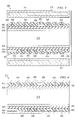
- FIGURE 3 illustrates a sectional side view of an exemplary SBU substrate 300 of the present invention.
- SBU substrate 300 comprises an underlying core substrate 310.
- a sequential build up process is used to place first metal conductor layer 320 on core substrate 310 and to place a first dielectric layer 330 on the first metal conductor layer 320.
- a sequential build up process is used to place first metal conductor layer 325 on core substrate 310 and to place a first dielectric layer 335 on the first metal conductor layer 325.
- Functional circuit elements 340 e.g., conductor lines 340
- filler circuit elements 350 are placed on first dielectric layer 330 using a prior art metal plate, pattern and etch process. Filler circuit elements 350 are placed on first dielectric layer 330 between functional circuit elements 340. The functional circuit elements 340 and the filler circuit elements 350 on first dielectric layer 330 are then covered with a second dielectric layer 360. Filler circuit elements 350 provide support for second dielectric layer 360 in areas in which functional circuit elements 340 are not present.
- circuit elements 345 e.g., conductor lines 345
- filler circuit elements 355 are placed on first dielectric layer 335 using a prior art metal plate, pattern and etch process. Filler circuit elements 355 are placed on first dielectric layer 335 between functional circuit elements 345. The functional circuit elements 345 and the filler circuit elements 355 on first dielectric layer 335 are then covered with a second dielectric layer 365. Filler circuit elements 355 provide support for second dielectric layer 365 in areas in which functional circuit elements 345 are not present.
- second dielectric layer 360 and second dielectric layer 365 are applied and then planarized to create a flat external surface on second dielectric layer 360 and to create a flat external surface on second dielectric layer 365.
- Second dielectric layer 360 and second dielectric layer 365 are applied in liquid form. Second dielectric layer 360 and second dielectric layer 365 are allowed to dry until they have solidified and are dry to touch. The external surface of second dielectric layer 360 is not flat due to the presence of the underlying functional circuit elements 340 and filler circuit elements 350. The external surface of second dielectric layer 365 is not flat due to the presence of the underlying functional circuit elements 345 and filler circuit elements 355.
- Planarization plate 370 is then placed in contact with the uneven external surface of second dielectric layer 360 and planarization plate 375 is then placed in contact with the uneven external surface of second dielectric layer 365.
- Planarization plate 370 contains heating element 372 so that planarization plate 370 is capable of heating second dielectric layer 360.
- Planarization plate 375 contains heating element 377 so that planarization plate 375 is capable of heating second dielectric layer 365.
- one or more heating elements may be provided that are separate from the planarization plates.
- heating element 372 may be located outside of planarization plate 370 and heating element 377 may be located outside of planarization plate 375.
- planarization plate 370 presses second dielectric layer 360
- the high portions (i.e., the elevated or protruding portions) of second dielectric layer 360 that are in contact with the surface of planarization plate 370 flatten and flow into the low portions or "valleys" in the surface of second dielectric layer 360.
- the high portions of second dielectric layer 360 fill up the low portions of second dielectric layer 360 so that a flat external surface may be formed on second dielectric layer 360.
- planarization plate 370 with respect to the external surface of second dielectric layer 360 is controlled by a conventional control mechanism (not shown) so that the surface 380 of planarization plate 370 may extend to but not extend beyond a control gap position (indicated in FIGURE 3 by dotted line 390).
- the location of the control gap position is chosen to select the final thickness of second dielectric layer 360. That is, the location of the control gap position will coincide with the final external surface of second dielectric layer 360.
- planarization plate 375 presses second dielectric layer 365
- the high portions of second dielectric layer 365 that are in contact with the surface of planarization plate 375 flatten and flow into the low portions or "valleys" in the surface of second dielectric layer 365.
- the high portions of second dielectric layer 365 fill up the low portions of second dielectric layer 365 so that a flat external surface may be formed on second dielectric layer 365.
- planarization plate 375 with respect to the external surface of second dielectric layer 365 is controlled by a conventional control mechanism (not shown) so that the surface 385 of planarization plate 375 may extend to but not extend beyond a control gap position (indicated in FIGURE 3 by dotted line 395).
- the location of the control gap position is chosen to select the final thickness of second dielectric layer 365. That is, the location of the control gap position will coincide with the final external surface of second dielectric layer 365.
- the two planes represented by dotted line 390 and by dotted line 395 are kept parallel with the surface area of SBU substrate 300 by conventional machine shop adjustment techniques.
- planarization plate 370 heats second dielectric layer 360, the dielectric material within second dielectric layer 360 flattens and hardens to form a flat external surface with respect to surface 380 of planarization plate 370.
- planarization plate 375 heats second dielectric layer 365, the dielectric material within second dielectric layer 365 flattens and hardens to form a flat external surface with respect to surface 385 of planarization plate 375.
- Planarization plate 370 is removed and the second dielectric layer 360 is allowed to cool.
- the heating element 372 of planarization plate 370 is turned off and the second dielectric layer 360 is allowed to cool while second dielectric layer 360 remains in contact with surface 380 of planarization plate 370. This sets a uniform thickness for second dielectric layer 360 in accordance with the location of the control gap position 390 as previously described.
- planarization plate 375 is removed and the second dielectric layer 365 is allowed to cool.
- the heating element 377 of planarization plate 375 is turned off and the second dielectric layer 365 is allowed to cool while second dielectric layer 365 remains in contact with surface 385 of planarization plate 375. This sets a uniform thickness for second dielectric layer 365 in accordance with the location of the control gap position 395 as previously described.
- planarization plate 370 and planarization plate 375 may simultaneously be placed in contact with their respective second dielectric layers 360 and 365. In this manner the top and bottom surfaces of substrate 300 may be simultaneously planarized.
- surface 380 of planarization plate 370 (and surface 385 of planarization plate 375) is machined to a high degree of flatness and sand blasted to a high degree of smoothness.
- a layer of non-stick material e.g., Teflon
- other techniques may be used such as impregnating surface 380 of planarization plate 370 and surface 385 of planarization plate 375 with non-stick material.
- FIGURE 4 illustrates a sectional side view of an advantageous embodiment of SBU substrate 300 of the present invention showing the result of applying an advantageous embodiment of the method of the present invention.
- SBU substrate 300 comprises second dielectric layer 360 having a flat exterior surface and second dielectric layer 365 having a flat exterior surface.
- a third metal conductor layer 400 has been applied to the flat exterior surface of second dielectric layer 360 and a third metal conductor layer 405 has been applied to the flat exterior surface of second dielectric layer 365.
- SBU substrate 300 of the present invention comprises third metal conductor layers, 400 and 405, that have flat external surfaces.
- the flatness of the external surfaces permits the third metal conductor layers, 400 and 405, to be etched to finer geometries than is possible in prior art SBU substrates that have layers with uneven external surfaces.
- the process described above may be repeated to add more layers.
- planarizing each dielectric layer after each metal etch process the external surface of the next deposited layer will be flatter than flat surfaces that may be achieved by prior art methods and can therefore be etched to finer geometries.
- FIGURE 5 illustrates a plan view of a portion 500 of an exemplary prior art SBU substrate 200 showing an exemplary substrate design.
- Functional circuit elements 240 of SBU substrate 200 are arranged in the exemplary substrate design as shown in FIGURE 5.
- the functional circuit elements 240 are represented by the dark shaded areas of portion 500.
- the substrate design of FIGURE 5 has a number of flat low areas or spaces between functional circuit elements 240. These flat low areas or spaces create uneven "gaps" between functional circuit elements 240. It is the presence of these "gaps" that create uneven surfaces during a sequential build up process in prior art SBU substrates.
- FIGURE 6 illustrates a plan view of a portion 600 of SBU substrate 300 of the present invention showing a substrate design identical to that shown in FIGURE 5.
- the functional circuit elements 340 are represented by the dark shaded areas of portion 600.
- FIGURE 6 also shows the placement of filler circuit elements 350 between functional circuit elements 340 of the present invention.
- the filler circuit elements 350 are represented by the light shaded areas of portion 600. The presence of filler circuit elements 350 between circuit elements 340 eliminates the "gaps" that would otherwise create uneven surfaces during the sequential build up process.
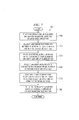
- FIGURE 7 illustrates a flow chart of an advantageous embodiment of a method of the present invention for providing mechanical planarization of a sequential build up substrate for an integrated circuit package.
- the steps of the method are generally denoted with reference numeral 700.
- first metal conductor layer 320 and first dielectric layer 330 have already been placed on underlying core substrate 310 of SBU substrate 300.
- Functional circuit elements 340 are then placed on the surface of first dielectric layer 330 (step 710).
- Filler circuit elements 350 are then placed between the functional circuit elements 340 on the surface of first dielectric layer 330 (step 720).
- second dielectric layer 360 is placed over functional circuit elements 340 and filler circuit elements 350 (step 730).
- the external surface of second dielectric layer 360 is uneven (i.e., not flat) due to the presence of functional circuit elements 340 and filler circuit elements 350.
- planarization plate 370 is placed in contact with the uneven external surface of second dielectric layer 360 (step 740). Heat from planarization plate 370 is then applied to the uneven external surface of second dielectric layer 360 to flatten the high portions of the second dielectric layer 360 to form a flat external surface (step 750). Lastly, metal conductor layer 400 is placed over the flat external surface of second dielectric surface 360 (step 760). This causes metal conductor layer 400 to have a flat external surface.
- the steps of the method may be repeated to add additional sequential build up layers to SBU substrate 300.
Landscapes
- Engineering & Computer Science (AREA)
- Manufacturing & Machinery (AREA)
- Microelectronics & Electronic Packaging (AREA)
- Production Of Multi-Layered Print Wiring Board (AREA)
Abstract
Description
Claims (19)
- A sequential buildup substrate comprising:a first dielectric layer;functional circuit elements placed on said first dielectric layer;filler circuit elements placed between said functional circuit elements on said first dielectric layer; anda second dielectric layer placed over said functional circuit elements and said filler circuit elements and said first dielectric layer wherein said second dielectric layer has a flat external surface.
- The sequential buildup substrate as set forth in Claim 1 further comprising a metal conductor layer placed over said flat external surface of said second dielectric layer.
- The sequential buildup substrate as set forth in Claim 2 wherein said metal conductor layer has a flat external surface.
- The sequential buildup substrate as set forth in Claim 1, 2 or 3 comprising a plurality of sequential buildup layers where each sequential buildup layer comprises:a first dielectric layer;functional circuit elements placed on said first dielectric layer;filler circuit elements placed between said functional circuit elements on said first dielectric layer;a second dielectric layer placed over said functional circuit elements and said filler circuit elements and said first dielectric layer wherein said second dielectric layer has a flat external surface; anda metal conductor layer placed over said flat external surface of said second dielectric layer.
- A sequential buildup substrate comprising:a core substrate;a first dielectric layer on a first side of said core substrate;a first set of functional circuit elements placed on said first dielectric layer;a first set of filler circuit elements placed between said first set of functional circuit elements on said first dielectric layer;a second dielectric layer on a second side of said core substrate;a second set of functional circuit elements placed on said second dielectric layer;a second set of filler circuit elements placed between said second set of functional circuit elements on said second dielectric layer;a third dielectric layer placed over said first set of functional circuit elements and over said first set of filler circuit elements and over said first dielectric layer wherein said third dielectric layer has a flat external surface; anda fourth dielectric layer placed over said second set of functional circuit elements and over said second set of filler circuit elements and over said second dielectric layer wherein said fourth dielectric layer has a flat external surface.
- The sequential buildup substrate as set forth in Claim 5 further comprising:a first metal conductor layer placed over said flat external surface of said third dielectric layer; anda second metal conductor layer placed over said flat external surface of said fourth dielectric layer.
- The sequential buildup substrate as set forth in Claim 6
wherein said first metal conductor layer has a flat external surface; and
wherein said second metal conductor layer has a flat external surface. - The sequential buildup substrate as set forth in Claim 5, 6 or 7 comprising a plurality of sequential buildup layers on a first side of said core substrate and a plurality of sequential buildup layers on a second side of said core substrate, where each sequential buildup layer comprises:a first dielectric layer;functional circuit elements placed on said first dielectric layer;filler circuit elements placed between said functional circuit elements on said first dielectric layer;a second dielectric layer placed over said functional circuit elements and said filler circuit elements and said first dielectric layer wherein said second dielectric layer has a flat external surface; anda metal conductor layer placed over said flat external surface of said second dielectric layer.
- In a sequential buildup substrate of the type comprising functional circuit elements placed on a first dielectric layer, a method for placing over said functional circuit elements a second dielectric layer having a flat external surface, said method comprising the steps of:placing filler circuit elements on said first dielectric layer between said functional circuit elements;placing a second dielectric layer over said functional circuit elements and over said filler circuit elements and over said first dielectric layer;placing a surface of a planarization plate in contact with an external surface of said second dielectric layer;heating said external surface of said second dielectric layer to flatten portions of said external surface of said second dielectric layer; andcooling said second dielectric layer to form a flat external surface on said second dielectric layer.
- The method as set forth in Claim 9 further comprising the step of:placing a metal conductor layer over said flat external surface of said second dielectric layer.
- The method as set forth in Claim 10 wherein said metal conductor layer has a flat external surface.
- The method as set forth in Claim 9, 10 or 11 further comprising the steps of:moving said planarization plate toward a control gap limit as said portions of said second dielectric layer flatten; andcausing said planarization plate to cease moving when said surface of said planarization plate that is in contact with said external surface of said second dielectric layer reaches said control gap limit.
- In a sequential buildup substrate of the type comprising a first set of functional circuit elements placed on a first dielectric layer on a first side of a core substrate and a second set of functional circuit elements placed on second dielectric layer on a second side of said core substrate, a method for placing over said first set of functional circuit elements a third dielectric layer having a flat external surface and placing over said second set of functional circuit elements a fourth dielectric layer having a flat external surface, said method comprising the steps of:placing a first set of filler circuit elements on said first dielectric layer between circuit elements of said first set of functional circuit elements;placing a second set of filler circuit elements on said second dielectric layer between circuit elements of said second set of functional circuit elements;placing a third dielectric layer over said first set of functional circuit elements and over said first set of filler circuit elements and over said first dielectric layer;placing a fourth dielectric layer over said second set of functional circuit elements and over said second set of filler circuit elements and over said second dielectric layer;placing a surface of a first planarization plate in contact with an external surface of said third dielectric layer;placing a surface of a second planarization plate in contact with an external surface of said fourth dielectric layer;heating said external surface of said third dielectric layer to flatten portions of said external surface of said third dielectric layer;heating said external surface of said fourth dielectric layer to flatten portions of said external surface of said fourth dielectric layer;cooling said third dielectric layer to form a flat external surface on said third dielectric layer; andcooling said fourth dielectric layer to form a flat external surface on said fourth dielectric layer.
- The method as set forth in Claim 13 further comprising the steps of:placing a first metal conductor layer over said flat external surface of said third dielectric layer; andplacing a second metal conductor layer over said flat external surface of said fourth dielectric layer.
- The method as set forth in Claim 13 or 14 wherein said first metal conductor layer has a flat external surface and said second metal conductor layer has a flat external surface.
- The method as set forth in Claim 13, 14 or 15 further comprising the steps of:moving said first planarization plate toward a first control gap limit as said portions of said third dielectric layer flatten;causing said first planarization plate to cease moving when said surface of said first planarization plate that is in contact with said external surface of said third dielectric layer reaches said first control gap limit;moving said second planarization plate toward a second control gap limit as said portions of said fourth dielectric layer flatten; andcausing said second planarization plate to cease moving when said surface of said second planarization plate that is in contact with said external surface of said fourth dielectric layer reaches said second control gap limit.
- The method as set forth in any of Claims 9 to 14 wherein said step of heating said external surface of said second, third and/or fourth dielectric layer to flatten portions of said external surface of said respective dielectric layer or layers comprises the step of:heating said external surface of said respective dielectric layer or layers with a heating element located within said second planarization plate.
- A method for providing mechanical planarization of a sequential build up package for an integrated circuit package of the type comprising functional circuit elements placed on a first dielectric layer, said method comprising the steps of:placing filler circuit elements on said first dielectric layer between said functional circuit elements;placing a second dielectric layer over said functional circuit elements and over said filler circuit elements;placing a surface of a planarization plate in contact with an external surface of said second dielectric layer;heating said external surface of said second dielectric layer to flatten portions of said external surface of said second dielectric layer;moving said planarization plate toward a control gap limit as said portions of said second dielectric layer flatten;causing said planarization plate to cease moving when said surface of said planarization plate that is in contact with said external surface of said second dielectric layer reaches said control gap limit;cooling said second dielectric layer to form a flat external surface on said second dielectric layer; andplacing a metal conductor layer over said flat external surface of said second dielectric layer, said metal conductor layer having a flat external surface.
- The method as set forth in Claim 18 further comprising the step of:creating a plurality of mechanically planarized sequential build up packages in said sequential buildup substrate by repeating the steps of Claim 19 for each mechanically planarized sequential build up package created in said sequential buildup substrate.
Applications Claiming Priority (2)
| Application Number | Priority Date | Filing Date | Title |
|---|---|---|---|
| US66422 | 2002-01-31 | ||
| US10/066,422 US6600227B1 (en) | 2002-01-31 | 2002-01-31 | System and method for providing mechanical planarization of a sequential build up substrate for an integrated circuit package |
Publications (2)
| Publication Number | Publication Date |
|---|---|
| EP1341231A2 true EP1341231A2 (en) | 2003-09-03 |
| EP1341231A3 EP1341231A3 (en) | 2006-07-19 |
Family
ID=27610484
Family Applications (1)
| Application Number | Title | Priority Date | Filing Date |
|---|---|---|---|
| EP20030250539 Withdrawn EP1341231A3 (en) | 2002-01-31 | 2003-01-29 | System and method for providing mechanical planarization of a sequential build up substrate for an integrated circuit package |
Country Status (3)
| Country | Link |
|---|---|
| US (1) | US6600227B1 (en) |
| EP (1) | EP1341231A3 (en) |
| JP (1) | JP2003234426A (en) |
Families Citing this family (2)
| Publication number | Priority date | Publication date | Assignee | Title |
|---|---|---|---|---|
| DE10253626A1 (en) * | 2002-11-15 | 2004-06-03 | Infineon Technologies Ag | Test structure for determining the electrical load capacity of contacts |
| US7775785B2 (en) * | 2006-12-20 | 2010-08-17 | Brewer Science Inc. | Contact planarization apparatus |
Family Cites Families (20)
| Publication number | Priority date | Publication date | Assignee | Title |
|---|---|---|---|---|
| JPH0642482B2 (en) * | 1984-11-15 | 1994-06-01 | 株式会社東芝 | Method for manufacturing semiconductor device |
| JPS63240045A (en) * | 1987-03-27 | 1988-10-05 | Matsushita Electric Ind Co Ltd | Semiconductor device |
| JPH0638551B2 (en) * | 1989-02-20 | 1994-05-18 | 松下電工株式会社 | Method for manufacturing multilayer wiring board |
| JPH0766552A (en) * | 1993-08-23 | 1995-03-10 | Hitachi Ltd | Wiring board manufacturing method |
| US5508233A (en) * | 1994-10-25 | 1996-04-16 | Texas Instruments Incorporated | Global planarization process using patterned oxide |
| US5821621A (en) * | 1995-10-12 | 1998-10-13 | Texas Instruments Incorporated | Low capacitance interconnect structure for integrated circuits |
| US5861342A (en) * | 1995-12-26 | 1999-01-19 | Vlsi Technology, Inc. | Optimized structures for dummy fill mask design |
| JP2973905B2 (en) * | 1995-12-27 | 1999-11-08 | 日本電気株式会社 | Method for manufacturing semiconductor device |
| US5783488A (en) * | 1996-01-31 | 1998-07-21 | Vlsi Technology, Inc. | Optimized underlayer structures for maintaining chemical mechanical polishing removal rates |
| US5798298A (en) * | 1996-02-09 | 1998-08-25 | United Microelectronics Corporation | Method of automatically generating dummy metals for multilevel interconnection |
| JPH10256707A (en) * | 1997-03-06 | 1998-09-25 | Ngk Spark Plug Co Ltd | Resin wiring board and method of manufacturing the same |
| JP3159108B2 (en) * | 1997-03-27 | 2001-04-23 | ヤマハ株式会社 | Semiconductor device and manufacturing method thereof |
| US6403385B1 (en) * | 1998-01-27 | 2002-06-11 | Advanced Micro Devices, Inc. | Method of inspecting a semiconductor wafer for defects |
| US6294456B1 (en) * | 1998-11-27 | 2001-09-25 | Taiwan Semiconductor Manufacturing Company | Method of prefilling of keyhole at the top metal level with photoresist to prevent passivation damage even for a severe top metal rule |
| US6274933B1 (en) * | 1999-01-26 | 2001-08-14 | Agere Systems Guardian Corp. | Integrated circuit device having a planar interlevel dielectric layer |
| US6218284B1 (en) * | 1999-02-01 | 2001-04-17 | United Microelectronics, Corp. | Method for forming an inter-metal dielectric layer |
| US6396089B1 (en) * | 1999-04-15 | 2002-05-28 | United Microelectronics Corp. | Semiconductor image sensor |
| JP3488839B2 (en) * | 1999-05-21 | 2004-01-19 | 株式会社野田スクリーン | Manufacturing method of printed wiring board |
| US6130149A (en) * | 1999-08-16 | 2000-10-10 | Taiwan Semiconductor Manufacturing Company | Approach for aluminum bump process |
| JP2002033581A (en) * | 2000-07-13 | 2002-01-31 | Mitsui Mining & Smelting Co Ltd | Manufacturing method of copper clad laminate |
-
2002
- 2002-01-31 US US10/066,422 patent/US6600227B1/en not_active Expired - Lifetime
-
2003
- 2003-01-29 EP EP20030250539 patent/EP1341231A3/en not_active Withdrawn
- 2003-01-31 JP JP2003023489A patent/JP2003234426A/en active Pending
Also Published As
| Publication number | Publication date |
|---|---|
| US20030141595A1 (en) | 2003-07-31 |
| EP1341231A3 (en) | 2006-07-19 |
| US6600227B1 (en) | 2003-07-29 |
| JP2003234426A (en) | 2003-08-22 |
Similar Documents
| Publication | Publication Date | Title |
|---|---|---|
| TWI250636B (en) | A semiconductor device and its fabrication method | |
| JP6624271B2 (en) | Mounting substrate wafer, multilayer ceramics substrate, mounting substrate, chip module, and method of manufacturing mounting substrate wafer | |
| TWI433626B (en) | Wiring substrate manufacturing method and printing mask | |
| US7633151B2 (en) | Integrated circuit package lid with a wetting film | |
| CN103199078A (en) | Multilayer electronic support structure with integrated structure constituent | |
| JPH11121645A (en) | Ceramic multilayer substrate and method of manufacturing the same | |
| CN101310374B (en) | Method for advanced solder bumping and system manufactured by said method | |
| US20060103024A1 (en) | Tiled construction of layered materials | |
| KR100782412B1 (en) | Transfer circuit forming method and circuit board manufacturing method | |
| JP4048019B2 (en) | Multilayer wiring board and manufacturing method thereof | |
| KR20010072143A (en) | Low-impedance high-density deposited-on-laminate structures having reduced stress | |
| CN112970102A (en) | Method of forming vias by micro-imprinting | |
| TWI732039B (en) | Manufacturing method of wiring board | |
| US6600227B1 (en) | System and method for providing mechanical planarization of a sequential build up substrate for an integrated circuit package | |
| US6808643B2 (en) | Hybrid interconnect substrate and method of manufacture thereof | |
| KR100970571B1 (en) | Contactor for semiconductor device test and manufacturing method | |
| KR101068466B1 (en) | Method for manufacturing unit substrate for lamination, multilayer substrate using unit substrate and method for manufacturing same | |
| JP4401527B2 (en) | Manufacturing method of semiconductor chip | |
| KR20130031592A (en) | Method for manuracturing printed circuit board with via and fine pitch circuit and printed circuit board by the same method | |
| WO2010104001A1 (en) | Method for manufacturing electronic device and apparatus for manufacturing electronic device | |
| KR20060070930A (en) | Manufacturing Method of Package Substrate | |
| CN116321677A (en) | Embedded circuit substrate and manufacturing method thereof | |
| CN215601549U (en) | Circuit board structure with support layers | |
| CN115863302A (en) | flat surface on the substrate | |
| JPH0638551B2 (en) | Method for manufacturing multilayer wiring board |
Legal Events
| Date | Code | Title | Description |
|---|---|---|---|
| PUAI | Public reference made under article 153(3) epc to a published international application that has entered the european phase |
Free format text: ORIGINAL CODE: 0009012 |
|
| AK | Designated contracting states |
Kind code of ref document: A2 Designated state(s): AT BE BG CH CY CZ DE DK EE ES FI FR GB GR HU IE IT LI LU MC NL PT SE SI SK TR |
|
| AX | Request for extension of the european patent |
Extension state: AL LT LV MK RO |
|
| PUAL | Search report despatched |
Free format text: ORIGINAL CODE: 0009013 |
|
| AK | Designated contracting states |
Kind code of ref document: A3 Designated state(s): AT BE BG CH CY CZ DE DK EE ES FI FR GB GR HU IE IT LI LU MC NL PT SE SI SK TR |
|
| AX | Request for extension of the european patent |
Extension state: AL LT LV MK RO |
|
| RIC1 | Information provided on ipc code assigned before grant |
Ipc: H01L 21/48 20060101AFI20060609BHEP |
|
| STAA | Information on the status of an ep patent application or granted ep patent |
Free format text: STATUS: THE APPLICATION HAS BEEN WITHDRAWN |
|
| 18W | Application withdrawn |
Effective date: 20061010 |