EP1341229A1 - Method for hermetic sealing of electronic parts - Google Patents
Method for hermetic sealing of electronic parts Download PDFInfo
- Publication number
- EP1341229A1 EP1341229A1 EP01997845A EP01997845A EP1341229A1 EP 1341229 A1 EP1341229 A1 EP 1341229A1 EP 01997845 A EP01997845 A EP 01997845A EP 01997845 A EP01997845 A EP 01997845A EP 1341229 A1 EP1341229 A1 EP 1341229A1
- Authority
- EP
- European Patent Office
- Prior art keywords
- solder
- electronic parts
- bonding
- cap
- sealing
- Prior art date
- Legal status (The legal status is an assumption and is not a legal conclusion. Google has not performed a legal analysis and makes no representation as to the accuracy of the status listed.)
- Withdrawn
Links
Images

Classifications
-
- B—PERFORMING OPERATIONS; TRANSPORTING
- B23—MACHINE TOOLS; METAL-WORKING NOT OTHERWISE PROVIDED FOR
- B23K—SOLDERING OR UNSOLDERING; WELDING; CLADDING OR PLATING BY SOLDERING OR WELDING; CUTTING BY APPLYING HEAT LOCALLY, e.g. FLAME CUTTING; WORKING BY LASER BEAM
- B23K35/00—Rods, electrodes, materials, or media, for use in soldering, welding, or cutting
- B23K35/22—Rods, electrodes, materials, or media, for use in soldering, welding, or cutting characterised by the composition or nature of the material
- B23K35/24—Selection of soldering or welding materials proper
- B23K35/30—Selection of soldering or welding materials proper with the principal constituent melting at less than 1550°C
- B23K35/3013—Au as the principal constituent
-
- H—ELECTRICITY
- H10—SEMICONDUCTOR DEVICES; ELECTRIC SOLID-STATE DEVICES NOT OTHERWISE PROVIDED FOR
- H10W—GENERIC PACKAGES, INTERCONNECTIONS, CONNECTORS OR OTHER CONSTRUCTIONAL DETAILS OF DEVICES COVERED BY CLASS H10
- H10W76/00—Containers; Fillings or auxiliary members therefor; Seals
- H10W76/60—Seals
-
- H—ELECTRICITY
- H10—SEMICONDUCTOR DEVICES; ELECTRIC SOLID-STATE DEVICES NOT OTHERWISE PROVIDED FOR
- H10W—GENERIC PACKAGES, INTERCONNECTIONS, CONNECTORS OR OTHER CONSTRUCTIONAL DETAILS OF DEVICES COVERED BY CLASS H10
- H10W95/00—Packaging processes not covered by the other groups of this subclass
-
- B—PERFORMING OPERATIONS; TRANSPORTING
- B23—MACHINE TOOLS; METAL-WORKING NOT OTHERWISE PROVIDED FOR
- B23K—SOLDERING OR UNSOLDERING; WELDING; CLADDING OR PLATING BY SOLDERING OR WELDING; CUTTING BY APPLYING HEAT LOCALLY, e.g. FLAME CUTTING; WORKING BY LASER BEAM
- B23K2101/00—Articles made by soldering, welding or cutting
- B23K2101/36—Electric or electronic devices
-
- H—ELECTRICITY
- H10—SEMICONDUCTOR DEVICES; ELECTRIC SOLID-STATE DEVICES NOT OTHERWISE PROVIDED FOR
- H10W—GENERIC PACKAGES, INTERCONNECTIONS, CONNECTORS OR OTHER CONSTRUCTIONAL DETAILS OF DEVICES COVERED BY CLASS H10
- H10W70/00—Package substrates; Interposers; Redistribution layers [RDL]
- H10W70/60—Insulating or insulated package substrates; Interposers; Redistribution layers
- H10W70/67—Insulating or insulated package substrates; Interposers; Redistribution layers characterised by their insulating layers or insulating parts
- H10W70/68—Shapes or dispositions thereof
- H10W70/682—Shapes or dispositions thereof comprising holes having chips therein
-
- H—ELECTRICITY
- H10—SEMICONDUCTOR DEVICES; ELECTRIC SOLID-STATE DEVICES NOT OTHERWISE PROVIDED FOR
- H10W—GENERIC PACKAGES, INTERCONNECTIONS, CONNECTORS OR OTHER CONSTRUCTIONAL DETAILS OF DEVICES COVERED BY CLASS H10
- H10W70/00—Package substrates; Interposers; Redistribution layers [RDL]
- H10W70/60—Insulating or insulated package substrates; Interposers; Redistribution layers
- H10W70/67—Insulating or insulated package substrates; Interposers; Redistribution layers characterised by their insulating layers or insulating parts
- H10W70/68—Shapes or dispositions thereof
- H10W70/685—Shapes or dispositions thereof comprising multiple insulating layers
-
- H—ELECTRICITY
- H10—SEMICONDUCTOR DEVICES; ELECTRIC SOLID-STATE DEVICES NOT OTHERWISE PROVIDED FOR
- H10W—GENERIC PACKAGES, INTERCONNECTIONS, CONNECTORS OR OTHER CONSTRUCTIONAL DETAILS OF DEVICES COVERED BY CLASS H10
- H10W72/00—Interconnections or connectors in packages
- H10W72/071—Connecting or disconnecting
- H10W72/075—Connecting or disconnecting of bond wires
-
- H—ELECTRICITY
- H10—SEMICONDUCTOR DEVICES; ELECTRIC SOLID-STATE DEVICES NOT OTHERWISE PROVIDED FOR
- H10W—GENERIC PACKAGES, INTERCONNECTIONS, CONNECTORS OR OTHER CONSTRUCTIONAL DETAILS OF DEVICES COVERED BY CLASS H10
- H10W72/00—Interconnections or connectors in packages
- H10W72/50—Bond wires
- H10W72/531—Shapes of wire connectors
- H10W72/536—Shapes of wire connectors the connected ends being ball-shaped
-
- H—ELECTRICITY
- H10—SEMICONDUCTOR DEVICES; ELECTRIC SOLID-STATE DEVICES NOT OTHERWISE PROVIDED FOR
- H10W—GENERIC PACKAGES, INTERCONNECTIONS, CONNECTORS OR OTHER CONSTRUCTIONAL DETAILS OF DEVICES COVERED BY CLASS H10
- H10W72/00—Interconnections or connectors in packages
- H10W72/50—Bond wires
- H10W72/531—Shapes of wire connectors
- H10W72/5363—Shapes of wire connectors the connected ends being wedge-shaped
-
- H—ELECTRICITY
- H10—SEMICONDUCTOR DEVICES; ELECTRIC SOLID-STATE DEVICES NOT OTHERWISE PROVIDED FOR
- H10W—GENERIC PACKAGES, INTERCONNECTIONS, CONNECTORS OR OTHER CONSTRUCTIONAL DETAILS OF DEVICES COVERED BY CLASS H10
- H10W72/00—Interconnections or connectors in packages
- H10W72/50—Bond wires
- H10W72/541—Dispositions of bond wires
- H10W72/5449—Dispositions of bond wires not being orthogonal to a side surface of the chip, e.g. fan-out arrangements
-
- H—ELECTRICITY
- H10—SEMICONDUCTOR DEVICES; ELECTRIC SOLID-STATE DEVICES NOT OTHERWISE PROVIDED FOR
- H10W—GENERIC PACKAGES, INTERCONNECTIONS, CONNECTORS OR OTHER CONSTRUCTIONAL DETAILS OF DEVICES COVERED BY CLASS H10
- H10W72/00—Interconnections or connectors in packages
- H10W72/851—Dispositions of multiple connectors or interconnections
- H10W72/874—On different surfaces
- H10W72/884—Die-attach connectors and bond wires
-
- H—ELECTRICITY
- H10—SEMICONDUCTOR DEVICES; ELECTRIC SOLID-STATE DEVICES NOT OTHERWISE PROVIDED FOR
- H10W—GENERIC PACKAGES, INTERCONNECTIONS, CONNECTORS OR OTHER CONSTRUCTIONAL DETAILS OF DEVICES COVERED BY CLASS H10
- H10W72/00—Interconnections or connectors in packages
- H10W72/90—Bond pads, in general
- H10W72/951—Materials of bond pads
-
- H—ELECTRICITY
- H10—SEMICONDUCTOR DEVICES; ELECTRIC SOLID-STATE DEVICES NOT OTHERWISE PROVIDED FOR
- H10W—GENERIC PACKAGES, INTERCONNECTIONS, CONNECTORS OR OTHER CONSTRUCTIONAL DETAILS OF DEVICES COVERED BY CLASS H10
- H10W76/00—Containers; Fillings or auxiliary members therefor; Seals
- H10W76/10—Containers or parts thereof
- H10W76/17—Containers or parts thereof characterised by their materials
-
- H—ELECTRICITY
- H10—SEMICONDUCTOR DEVICES; ELECTRIC SOLID-STATE DEVICES NOT OTHERWISE PROVIDED FOR
- H10W—GENERIC PACKAGES, INTERCONNECTIONS, CONNECTORS OR OTHER CONSTRUCTIONAL DETAILS OF DEVICES COVERED BY CLASS H10
- H10W90/00—Package configurations
- H10W90/701—Package configurations characterised by the relative positions of pads or connectors relative to package parts
- H10W90/731—Package configurations characterised by the relative positions of pads or connectors relative to package parts of die-attach connectors
- H10W90/734—Package configurations characterised by the relative positions of pads or connectors relative to package parts of die-attach connectors between a chip and a stacked insulating package substrate, interposer or RDL
-
- H—ELECTRICITY
- H10—SEMICONDUCTOR DEVICES; ELECTRIC SOLID-STATE DEVICES NOT OTHERWISE PROVIDED FOR
- H10W—GENERIC PACKAGES, INTERCONNECTIONS, CONNECTORS OR OTHER CONSTRUCTIONAL DETAILS OF DEVICES COVERED BY CLASS H10
- H10W90/00—Package configurations
- H10W90/701—Package configurations characterised by the relative positions of pads or connectors relative to package parts
- H10W90/751—Package configurations characterised by the relative positions of pads or connectors relative to package parts of bond wires
- H10W90/754—Package configurations characterised by the relative positions of pads or connectors relative to package parts of bond wires between a chip and a stacked insulating package substrate, interposer or RDL
Definitions
- the present invention relates to a method of hermetically sealing electronic parts by which a container (base) having semiconductor devices placed thereon and a cap are bonded together via a solder. More particularly, it relates to a method of hermetic sealing that can reduce the leak rate to not more than one tenth of levels under conventional methods.
- solder sealing method As the hermetic sealing technology of semiconductor devices, the solder sealing method, seam welding method, laser sealing method, etc., are known, and these methods are appropriately used according to the scale of electronic parts to be manufactured, required sealing performance, etc.
- the solder sealing method involves soldering a cap to a base on which semiconductor devices are mounted, and sealing the semiconductor devices by covering them. Because it is unnecessary to limit container materials and their thickness unlike the seam welding method and because expensive bonding devices required by the laser sealing method are unnecessary, this solder sealing method has come into widespread use as a method that allows a high-level sealed state to be realized at appropriate cost.
- the invention was made in consideration of a situation as mentioned above, and it is the object of the invention to provide a hermetic sealing technique of electronic parts, which permits hermetic sealing by the solder sealing method at a lower leak rate and more efficiently than with conventional methods, and which does not cause leakage even in the trend toward smaller-size electronic parts in the future.
- the present inventors has made intensive investigations to solve the above-described problem and decided to review solder materials used in the conventional solder sealing method. This is because existing equipment can be used without a modification and addition of new equipment is unnecessary if a change is made only in the solder materials.
- solder materials used in the solder sealing method Sn-Pb-based solders (Sn-37 wt.% Pb) are mostly used and Au-Sn-based solders (Au-20 wt.% Sn) are sometimes used.
- the present inventors decided to use Au-Sn-based solders as the basic composition of solder materials. This is based on the conception that Pb, which is an element that presents a danger to the human body, is not a desirable material in view of the safety to workers and the standpoint of environmental conservation of the recent times.
- Au-Sn-based solders Au-20 wt. % Sn
- the inventors closely examined the bonded portions obtained by Au-20 wt.% Sn solders, and found out that the bonded portions obtained by the solder materials basically show an Au-Sn eutectic microstructure with a partial mixture of an Au-Sn alloy phase having a high concentration of Au (hereinafter referred to as an Au rich phase) . Because this Au rich phase is a kind of intermetallic compound and is hard, it has a higher melting point than the surrounding Au-Sn eutectic phase. At temperatures below the bonding temperature of a cap, therefore, this Au rich phase does not melt and remains as a hard phase.
- This nonuniformity of the solder layer is not a direct cause of leakage.
- the nonuniformity of the solder layer is remarkable, it might be thought that leakage occurs from portions of small solder layer thickness due to the deterioration of the solder layer resulting from use of electronic parts for a long time or due to a pressure difference that occurs in and outside electronic parts during a leak test.
- the amount of solder used also decreases and hence the effect of an Au rich phase becomes great. In this case, there is a fear that portions of defective bonding might be formed and that bonded portions whose air-tight state cannot be maintained even immediately after bonding might be formed.
- a method of hermetically sealing electronic parts that includes the step of bonding a base, on which semiconductor devices are mounted, and a cap together via a solder, in which this solder consists, by weight, of 78% or more but less than 79.5% Au, and the balance Sn.
- the Au content was slightly changed from those of conventionally used Au-Sn-based solders and by this slight change the microstructure of the solder during solidification can be almost converted to an Au-Sn eutectic structure.
- an Au rich phase is not formed in the solder layer during bonding and uniform thickness can be given to the solder layer.
- leakage does not occur during use for a long period or during a leak test.
- the content of Au of the solder to be used is limited to a narrow range of 78 wt.% or more but less than 79.5 wt.% is as follows.
- Au rich crystals are formed in large amounts when the Au content is not less than 79.5 wt.%, whereas Sn rich crystals begin to be formed when the Au content is less than 78 wt.% and, also in this case, the formation of Sn rich crystals has an adverse effect on bonded portions.
- Sn rich crystals are formed in small amounts. However, because the Sn rich crystals are fine, they do not make the solder layer thickness nonuniform if they are formed in small amounts.
- solder composition composed, by weight, of 78% or more but 79% or less Au, and the balance Sn, as the solder described in a second aspect of the present invention.
- the reason why the cap is plated with gold and why besides the solder composition is made narrower than the range described in Claim 1 is that the wettability of the cap is improved by plating the cap with gold and that, at the same time, the formation of an Au rich phase caused by this plating with gold is suppressed. That is, when the cap is plated with gold, the solder and the gold coating layer come into contact with each other and gold is diffused in the solder, resulting in an increase in the gold content of the solder. As a result, an Au rich phase may sometimes be formed.
- the Au coming from the coating layer is diffused into an Sn rich phase that is formed in a small amount due to this composition, whereby the microstructure of the solder is formed as an Au-Sn eutectic structure.
- the second aspect of the invention it is possible to ensure bonding strength by improving the wettability to the cap and, at the same time, it is possible to ensure a uniform solder layer thickness by suppressing the formation of an Au rich phase.
- Embodiment A 78.5 wt.% Au-21.5 wt.% Sn ingot obtained by a melting-casting process was rolled into a sheet and after that, a solder in square ring form was obtained through punching. This solder was employed to bond a cap to a base on which IC chips are mounted, whereby an IC package was produced.
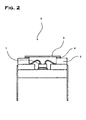
- a base 2 made of ceramics, on which an IC 1 is mounted, and a cap 3 made of Kovar and previously plated with Au was sandwiched a solder 4 after the above-described working, and they were heated in a conveyor furnace to 300°C, whereby the solder 4 was melted and bonded to obtain an IC package 5.
- the section of the IC package after bonding is shown in Fig. 2.
- Comparative example In contrast to the embodiment, an 80 wt.%-Au-20 wt.% Sn brazing material was produced and an IC package was produced.
- the method of producing the brazing material, method of working the brazing material and method of producing the IC package were the same as in the above embodiment.
- Example of experiment 1 (measurement of leak rate) :
- the IC packages produced in the above-described embodiment and comparative example were subjected to a helium leak test, which is a fine leak test.
- the leak rates of the IC packages produced in the embodiment and comparative example were compared and examined.
- the helium leak test was conducted by applying the IC packages thus produced to a helium detector, causing the helium molecules in the interior to leak out through drawing a vacuum in the exterior of the IC packages, and counting the leaking helium molecules.
- the leak rate (fraction defective) was 0.2% in the IC package produced with the use of the 80 wt.%-Au-20 wt.% Sn brazing material of the comparative example.
- the leak rate of the IC package produced in the embodiment was 0.1% and it was confirmed that the leak rate is improved from that of the hermetic sealing method of comparative example.
- Example of experiment 2 observation of microstructures of bonded portions
- the two bonded portions were observed under an SEM.
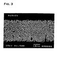
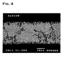
- the SEM photographs of the bonded portions of embodiment and comparative example are shown in Fig.s 3 and 4, respectively. From these SEM photographs it was ascertained that the bonded portion of the embodiment has a fine eutectic structure.
- coarse Au rich phases the white parts in Fig. 4 are present in the bonded portion of the comparative example. Because these Au rich phases have different sizes, it might be thought that they make the solder layer thickness during bonding nonuniform, though slightly, thereby causing leakage.
- the present invention makes it possible to hermetically seal electronic parts without generating an Au rich phase that makes the solder layer thickness after bonding non-uniform. This enables the leak rate of electronic parts to be lowered from levels of conventional ones, making it possible to efficiently manufacture electronic parts. Further in the future, the invention is adaptable for the miniaturization of electronic parts.
Landscapes
- Engineering & Computer Science (AREA)
- Mechanical Engineering (AREA)
- Piezo-Electric Or Mechanical Vibrators, Or Delay Or Filter Circuits (AREA)
- Wire Bonding (AREA)
- Ceramic Products (AREA)
Abstract
There is provided a method of hermetically sealing
electronic parts, comprising the step of bonding a base
having semiconductor devices mounted thereon and a cap
together via a solder. The solder is composed, by weight,
of 78% or more but less than 79.5% Au, and the balance Sn.
It is particularly preferred that the bonding is performed
with the use of a solder composition composed, by weight,
of 78% or more but 79% or less Au, and the balance Sn as the
solder and furthermore through plating the cap with gold.
Description
The present invention relates to a method of
hermetically sealing electronic parts by which a container
(base) having semiconductor devices placed thereon and a cap
are bonded together via a solder. More particularly, it
relates to a method of hermetic sealing that can reduce the
leak rate to not more than one tenth of levels under
conventional methods.
In various semiconductor devices, such as SAW filters
and quartz-crystal oscillators, if they are kept as they are,
there is a fear that due to the oxygen and humidity in the
air, their conductive patterns and pads might be corroded,
resulting in poor properties. Therefore, in order to
completely cut off these semiconductor devices from the
outside air, usually they are mounted on eleotronic apparatus
while being hermetically sealed in a metal or ceramic
container (package), the interior of which is in a vacuum
or is filled with He or N2.
As the hermetic sealing technology of semiconductor
devices, the solder sealing method, seam welding method,
laser sealing method, etc., are known, and these methods are
appropriately used according to the scale of electronic parts
to be manufactured, required sealing performance, etc.
Among others, the solder sealing method involves soldering
a cap to a base on which semiconductor devices are mounted,
and sealing the semiconductor devices by covering them.
Because it is unnecessary to limit container materials and
their thickness unlike the seam welding method and because
expensive bonding devices required by the laser sealing
method are unnecessary, this solder sealing method has come
into widespread use as a method that allows a high-level
sealed state to be realized at appropriate cost.
Incidentally, for electronic parts for which the
above-described sealed state is required, needless to say,
it is necessary that the semiconductor devices in the
interior be completely cut off from the outside air and be
used without a fear of the generation of leakage. In the
manufacturing processes of electronic parts by use of these
hermetic sealing techniques, a test called the fine leak test
is conducted in order to measure the leak rate of products.
This test enables even very minutes leaks of not more than
10-6 atm/cc·sec to be captured and defective parts that do
not meet this standard are rejected to guarantee the
reliability of electronic parts.
And even for electronic parts of which such a high
sealing property is required, through the use of the solder
sealing method it is possible to efficiently manufacture
electronic parts at a leak rate (fraction defective) of not
more than 0.2%. However, in order to further reduce the cost
of electronic parts, it is desirable that this leak rate be
capable of further reduced.
On the other hand, due to the continuing requirement
for smaller-size electronic apparatus of the recent years,
it is required that electronic parts to be mounted on these
electronic apparatus be also smaller in size. However, when
the size of electronic parts is reduced to meet this
requirement, the hermetically sealing the electronic parts
becomes difficult. When the requirement for a reduction in
the fraction defective is considered in addition to this
requirement for small size design, it can be said that also
for the solder sealing method, a method with a low rate of
poor sealing is sought for more readily.
The invention was made in consideration of a situation
as mentioned above, and it is the object of the invention
to provide a hermetic sealing technique of electronic parts,
which permits hermetic sealing by the solder sealing method
at a lower leak rate and more efficiently than with
conventional methods, and which does not cause leakage even
in the trend toward smaller-size electronic parts in the
future.
The present inventors has made intensive investigations
to solve the above-described problem and decided to review
solder materials used in the conventional solder sealing
method. This is because existing equipment can be used
without a modification and addition of new equipment is
unnecessary if a change is made only in the solder materials.
As the solder materials used in the solder sealing method,
Sn-Pb-based solders (Sn-37 wt.% Pb) are mostly used and
Au-Sn-based solders (Au-20 wt.% Sn) are sometimes used. The
present inventors decided to use Au-Sn-based solders as the
basic composition of solder materials. This is based on the
conception that Pb, which is an element that presents a danger
to the human body, is not a desirable material in view of
the safety to workers and the standpoint of environmental
conservation of the recent times.
And the inventors considered that in using Au-Sn-based
solders (Au-20 wt. % Sn) as solder materials, it is necessary
to change their compositions in order to ensure higher-reliability
sealing than before. This is because although
Au-20 wt. % Sn solders have the advantage that they have no
effect of sealing on the bonded portions of semiconductor
devices, leakage may sometimes occur, though not frequently,
because of their relatively low melting points of about
280°C.
And the inventors closely examined the bonded portions
obtained by Au-20 wt.% Sn solders, and found out that the
bonded portions obtained by the solder materials basically
show an Au-Sn eutectic microstructure with a partial mixture
of an Au-Sn alloy phase having a high concentration of Au
(hereinafter referred to as an Au rich phase) . Because this
Au rich phase is a kind of intermetallic compound and is hard,
it has a higher melting point than the surrounding Au-Sn
eutectic phase. At temperatures below the bonding
temperature of a cap, therefore, this Au rich phase does not
melt and remains as a hard phase. And because of diverse
sizes of this Au rich phase, even if a cap is bonded to a
base under uniform pressure, Au rich phases of various sizes
adhere to the bonded surfaces of the cap or base, with the
result that areas of small solder layer thickness and those
of large solder layer thickness are formed, leading to a
nonuniform thickness of the solder layer.
This nonuniformity of the solder layer is not a direct
cause of leakage. However, when the nonuniformity of the
solder layer is remarkable, it might be thought that leakage
occurs from portions of small solder layer thickness due to
the deterioration of the solder layer resulting from use of
electronic parts for a long time or due to a pressure
difference that occurs in and outside electronic parts during
a leak test. Also, it might be thought that when the sizes
of electronic parts are reduced in the future, the amount
of solder used also decreases and hence the effect of an Au
rich phase becomes great. In this case, there is a fear that
portions of defective bonding might be formed and that bonded
portions whose air-tight state cannot be maintained even
immediately after bonding might be formed.
When this effect of an Au rich phase is considered, it
is also conceivable that a high temperature at which the Au
rich phase can also be melted and at which the solder is a
complete liquid phase is used as the bonding temperature of
the cap, i.e., the heating temperature of the solder.
However, raising the bonding temperature results in an
adverse effect on the semiconductor devices in the interior
and, therefore, it cannot be said that this is an appropriate
means. Therefore, considering that a drastic review of
solder compositions is necessary for preventing an Au rich
phase from being formed in the melting and solidification
processes while keeping the bolding temperature in the same
range as before, the inventors conducted an investigation
and, as a result, they reached the present invention.
In the invention there is provided a method of
hermetically sealing electronic parts that includes the step
of bonding a base, on which semiconductor devices are mounted,
and a cap together via a solder, in which this solder consists,
by weight, of 78% or more but less than 79.5% Au, and the
balance Sn.
In the invention, the Au content was slightly changed
from those of conventionally used Au-Sn-based solders and
by this slight change the microstructure of the solder during
solidification can be almost converted to an Au-Sn eutectic
structure. As a result, an Au rich phase is not formed in
the solder layer during bonding and uniform thickness can
be given to the solder layer. As a result, leakage does not
occur during use for a long period or during a leak test.
As a result, it becomes possible to lower the leak ratio
(fraction defective) of bonded portions from conventional
levels and to efficiently manufacture electronic parts.
The reason why in the invention the content of Au of
the solder to be used is limited to a narrow range of 78 wt.%
or more but less than 79.5 wt.% is as follows. Au rich
crystals are formed in large amounts when the Au content is
not less than 79.5 wt.%, whereas Sn rich crystals begin to
be formed when the Au content is less than 78 wt.% and, also
in this case, the formation of Sn rich crystals has an adverse
effect on bonded portions. Also with the composition of the
invention, Sn rich crystals are formed in small amounts.
However, because the Sn rich crystals are fine, they do not
make the solder layer thickness nonuniform if they are formed
in small amounts.
Incidentally, in bonding techniques using solders as
in the solder sealing method, it is desirable to improve the
wettability of solders in order to ensure the bonding
strength of bonded members. In particular, as a material
for caps used in electronic parts, Kovar (brand name of a
54 wt.% Fe-29 wt.% Ni-17 wt.% Co alloy) is often used.
However, because Kovar is not wetted by solders, bonding
defects and solder exfoliation might occur if bonding is
performed by directly applying solders to a cap made of Kovar.
Therefore, in order to ensure the wettability of solders and
a uniform solder layer thickness by preventing the generation
of an Au rich phase in solders, it is desirable to perform
bonding by plating the cap with gold and by using a solder
composition composed, by weight, of 78% or more but 79% or
less Au, and the balance Sn, as the solder described in a
second aspect of the present invention.
The reason why the cap is plated with gold and why besides
the solder composition is made narrower than the range
described in Claim 1 is that the wettability of the cap is
improved by plating the cap with gold and that, at the same
time, the formation of an Au rich phase caused by this plating
with gold is suppressed. That is, when the cap is plated
with gold, the solder and the gold coating layer come into
contact with each other and gold is diffused in the solder,
resulting in an increase in the gold content of the solder.
As a result, an Au rich phase may sometimes be formed. For
this reason, by using an Au content of solder in the range,
by weight, of 78.5% or more and 79% or less, the Au coming
from the coating layer is diffused into an Sn rich phase that
is formed in a small amount due to this composition, whereby
the microstructure of the solder is formed as an Au-Sn
eutectic structure.
Therefore, according to the second aspect of the
invention, it is possible to ensure bonding strength by
improving the wettability to the cap and, at the same time,
it is possible to ensure a uniform solder layer thickness
by suppressing the formation of an Au rich phase.
The embodiment of the invention will be described below
in connection with the drawings.
Embodiment: A 78.5 wt.% Au-21.5 wt.% Sn ingot obtained by
a melting-casting process was rolled into a sheet and after
that, a solder in square ring form was obtained through
punching. This solder was employed to bond a cap to a base
on which IC chips are mounted, whereby an IC package was
produced. As shown in Fig. 1, between a base 2 made of
ceramics, on which an IC 1 is mounted, and a cap 3 made of
Kovar and previously plated with Au was sandwiched a solder
4 after the above-described working, and they were heated
in a conveyor furnace to 300°C, whereby the solder 4 was melted
and bonded to obtain an IC package 5. The section of the
IC package after bonding is shown in Fig. 2.
Comparative example: In contrast to the embodiment, an 80
wt.%-Au-20 wt.% Sn brazing material was produced and an IC
package was produced. The method of producing the brazing
material, method of working the brazing material and method
of producing the IC package were the same as in the above
embodiment.
Example of experiment 1 (measurement of leak rate) : The IC
packages produced in the above-described embodiment and
comparative example were subjected to a helium leak test,
which is a fine leak test. The leak rates of the IC packages
produced in the embodiment and comparative example were
compared and examined. Incidentally, the helium leak test
was conducted by applying the IC packages thus produced to
a helium detector, causing the helium molecules in the
interior to leak out through drawing a vacuum in the exterior
of the IC packages, and counting the leaking helium
molecules.
As a result, the leak rate (fraction defective) was 0.2%
in the IC package produced with the use of the 80 wt.%-Au-20
wt.% Sn brazing material of the comparative example. In
contrast to this, the leak rate of the IC package produced
in the embodiment was 0.1% and it was confirmed that the leak
rate is improved from that of the hermetic sealing method
of comparative example.
Example of experiment 2 (observation of microstructures of
bonded portions): Next, in order to investigate the
microstructures (solder layers) of the IC packages produced
in the embodiment and comparative example, the two bonded
portions were observed under an SEM. The SEM photographs
of the bonded portions of embodiment and comparative example
are shown in Fig.s 3 and 4, respectively. From these SEM
photographs it was ascertained that the bonded portion of
the embodiment has a fine eutectic structure. On the other
hand, it was ascertained that coarse Au rich phases (the white
parts in Fig. 4) are present in the bonded portion of the
comparative example. Because these Au rich phases have
different sizes, it might be thought that they make the solder
layer thickness during bonding nonuniform, though slightly,
thereby causing leakage.
As described above, the present invention makes it
possible to hermetically seal electronic parts without
generating an Au rich phase that makes the solder layer
thickness after bonding non-uniform. This enables the leak
rate of electronic parts to be lowered from levels of
conventional ones, making it possible to efficiently
manufacture electronic parts. Further in the future, the
invention is adaptable for the miniaturization of electronic
parts.
Claims (2)
- A method of hermetically sealing electronic parts, said method comprising the step of bonding a base having semiconductor devices mounted thereon and a cap together via a solder, wherein said bonding is performed with the use of said solder composition composed, by weight, of 78% or more but less than 79.5% Au, and the balance Sn.
- The method of hermetically sealing electronic parts according to Claim 1, wherein said bonding is performed through plating the cap with gold and with the use of said solder composition composed, by weight, of 78% or more but less than 79% Au, and the balance Sn.
Applications Claiming Priority (3)
| Application Number | Priority Date | Filing Date | Title |
|---|---|---|---|
| JP2000358744A JP2001176999A (en) | 2000-11-27 | 2000-11-27 | Hermetic sealing method for electronic components |
| JP2000358744 | 2000-11-27 | ||
| PCT/JP2001/010302 WO2002043141A1 (en) | 2000-11-27 | 2001-11-27 | Method for hermetic sealing of electronic parts |
Publications (2)
| Publication Number | Publication Date |
|---|---|
| EP1341229A1 true EP1341229A1 (en) | 2003-09-03 |
| EP1341229A4 EP1341229A4 (en) | 2005-08-24 |
Family
ID=18830592
Family Applications (1)
| Application Number | Title | Priority Date | Filing Date |
|---|---|---|---|
| EP01997845A Withdrawn EP1341229A4 (en) | 2000-11-27 | 2001-11-27 | METHOD FOR HERMETIC SEALING OF ELECTRONIC PARTS |
Country Status (7)
| Country | Link |
|---|---|
| US (1) | US6691911B2 (en) |
| EP (1) | EP1341229A4 (en) |
| JP (1) | JP2001176999A (en) |
| KR (1) | KR100501505B1 (en) |
| CN (1) | CN1394359A (en) |
| TW (1) | TW508683B (en) |
| WO (1) | WO2002043141A1 (en) |
Cited By (1)
| Publication number | Priority date | Publication date | Assignee | Title |
|---|---|---|---|---|
| CN102267022A (en) * | 2011-07-27 | 2011-12-07 | 重庆群崴电子材料有限公司 | Lead-free tin-gold alloy solder for photoelectric packaging and method for manufacturing lead-free tin-gold alloy solder |
Families Citing this family (16)
| Publication number | Priority date | Publication date | Assignee | Title |
|---|---|---|---|---|
| US6820797B2 (en) * | 2002-11-27 | 2004-11-23 | Agilent Technologies, Inc. | System and method for seal formation |
| DE602005005733T2 (en) | 2004-02-20 | 2009-05-28 | Tanaka Kikinzoku Kogyo K.K. | Joining method by means of an Au-Sn brazing material whose thickness i.a. depends on the Sn content |
| JP4769469B2 (en) * | 2004-02-20 | 2011-09-07 | 田中貴金属工業株式会社 | Bonding method using Au-Sn brazing material |
| JP4285753B2 (en) * | 2004-06-21 | 2009-06-24 | 田中貴金属工業株式会社 | Hermetic seal cover and method for manufacturing the same |
| JP4560830B2 (en) * | 2004-06-28 | 2010-10-13 | 三菱マテリアル株式会社 | Au-Sn alloy powder for solder paste |
| JP2007142054A (en) * | 2005-11-16 | 2007-06-07 | Sumitomo Metal Mining Co Ltd | Seal cover and manufacturing method thereof |
| JP4826735B2 (en) * | 2005-11-21 | 2011-11-30 | 三菱マテリアル株式会社 | Manufacturing method of Au-Sn alloy bump without incorporating large voids |
| US7910945B2 (en) * | 2006-06-30 | 2011-03-22 | Cree, Inc. | Nickel tin bonding system with barrier layer for semiconductor wafers and devices |
| US7855459B2 (en) * | 2006-09-22 | 2010-12-21 | Cree, Inc. | Modified gold-tin system with increased melting temperature for wafer bonding |
| US20100006336A1 (en) * | 2007-05-11 | 2010-01-14 | Tomohiro Shimada | Lid or case for sealed package and method for manufacturing the same |
| JP5145964B2 (en) * | 2008-01-18 | 2013-02-20 | 株式会社大真空 | Electronic component body housing member, electronic component, and method of manufacturing electronic component |
| CN101819076B (en) * | 2010-04-21 | 2011-07-27 | 中国电子科技集团公司第二十四研究所 | Sn/Au eutectic based chip partial vacuum packaging method of resonance type pressure sensor |
| JP5906811B2 (en) * | 2012-02-29 | 2016-04-20 | 沖電気工業株式会社 | Package and power amplifier |
| JP6477421B2 (en) | 2015-10-29 | 2019-03-06 | 三菱電機株式会社 | Semiconductor device |
| JP6915556B2 (en) * | 2018-01-24 | 2021-08-04 | 三菱マテリアル株式会社 | Bonding layer of semiconductor module, semiconductor module and its manufacturing method |
| US10574025B2 (en) * | 2018-01-26 | 2020-02-25 | Lightwave Logic Inc. | Hermetic capsule and method for a monolithic photonic integrated circuit |
Family Cites Families (21)
| Publication number | Priority date | Publication date | Assignee | Title |
|---|---|---|---|---|
| US3340602A (en) * | 1965-02-01 | 1967-09-12 | Philco Ford Corp | Process for sealing |
| US3648357A (en) * | 1969-07-31 | 1972-03-14 | Gen Dynamics Corp | Method for sealing microelectronic device packages |
| US4356047A (en) * | 1980-02-19 | 1982-10-26 | Consolidated Refining Co., Inc. | Method of making ceramic lid assembly for hermetic sealing of a semiconductor chip |
| US4418857A (en) * | 1980-12-31 | 1983-12-06 | International Business Machines Corp. | High melting point process for Au:Sn:80:20 brazing alloy for chip carriers |
| US4772935A (en) * | 1984-12-19 | 1988-09-20 | Fairchild Semiconductor Corporation | Die bonding process |
| JPS61204953A (en) * | 1985-03-08 | 1986-09-11 | Sumitomo Metal Mining Co Ltd | Hermetic sealing cover and manufacture thereof |
| US4746583A (en) * | 1986-11-21 | 1988-05-24 | Indium Corporation | Ceramic combined cover |
| US4833102A (en) * | 1987-03-17 | 1989-05-23 | National Semiconductor Corporation | Process of making a ceramic lid for use in a hermetic seal package |
| US4769272A (en) * | 1987-03-17 | 1988-09-06 | National Semiconductor Corporation | Ceramic lid hermetic seal package structure |
| GB8807729D0 (en) * | 1988-03-31 | 1988-05-05 | British Telecomm | Device mounting |
| JP3086086B2 (en) | 1992-10-19 | 2000-09-11 | 田中貴金属工業株式会社 | How to join lead pins to circuit terminals |
| JP2518508B2 (en) * | 1993-04-14 | 1996-07-24 | 日本電気株式会社 | Semiconductor device |
| US5465008A (en) * | 1993-10-08 | 1995-11-07 | Stratedge Corporation | Ceramic microelectronics package |
| US5550398A (en) * | 1994-10-31 | 1996-08-27 | Texas Instruments Incorporated | Hermetic packaging with optical |
| US5622305A (en) * | 1995-05-10 | 1997-04-22 | Lucent Technologies Inc. | Bonding scheme using group VB metallic layer |
| JP3593185B2 (en) * | 1995-07-21 | 2004-11-24 | Necトーキン株式会社 | Optoelectronic components |
| JPH09122969A (en) * | 1996-09-27 | 1997-05-13 | Tokuriki Honten Co Ltd | Au-sn brazing filler metal |
| US5770890A (en) * | 1997-02-25 | 1998-06-23 | Raytheon Company | Using a thermal barrier to provide a hermetic seal surface on aluminum nitride substrate electronic packages |
| KR19990029741A (en) * | 1997-09-29 | 1999-04-26 | 갈라스 윌리엄 이 | How to solder without flux using gold plated solder material and solder |
| US6303986B1 (en) * | 1998-07-29 | 2001-10-16 | Silicon Light Machines | Method of and apparatus for sealing an hermetic lid to a semiconductor die |
| SE512906C2 (en) * | 1998-10-02 | 2000-06-05 | Ericsson Telefon Ab L M | Procedure for soldering a semiconductor chip and RF power transistor for conducting it |
-
2000
- 2000-11-27 JP JP2000358744A patent/JP2001176999A/en active Pending
-
2001
- 2001-10-31 TW TW090127001A patent/TW508683B/en not_active IP Right Cessation
- 2001-11-27 CN CN01803410A patent/CN1394359A/en active Pending
- 2001-11-27 EP EP01997845A patent/EP1341229A4/en not_active Withdrawn
- 2001-11-27 US US10/149,746 patent/US6691911B2/en not_active Expired - Lifetime
- 2001-11-27 KR KR10-2002-7007912A patent/KR100501505B1/en not_active Expired - Lifetime
- 2001-11-27 WO PCT/JP2001/010302 patent/WO2002043141A1/en not_active Ceased
Cited By (1)
| Publication number | Priority date | Publication date | Assignee | Title |
|---|---|---|---|---|
| CN102267022A (en) * | 2011-07-27 | 2011-12-07 | 重庆群崴电子材料有限公司 | Lead-free tin-gold alloy solder for photoelectric packaging and method for manufacturing lead-free tin-gold alloy solder |
Also Published As
| Publication number | Publication date |
|---|---|
| WO2002043141A1 (en) | 2002-05-30 |
| US20020190106A1 (en) | 2002-12-19 |
| EP1341229A4 (en) | 2005-08-24 |
| KR20020063596A (en) | 2002-08-03 |
| TW508683B (en) | 2002-11-01 |
| US6691911B2 (en) | 2004-02-17 |
| CN1394359A (en) | 2003-01-29 |
| KR100501505B1 (en) | 2005-07-18 |
| JP2001176999A (en) | 2001-06-29 |
Similar Documents
| Publication | Publication Date | Title |
|---|---|---|
| US6691911B2 (en) | Method for hermetic sealing of electronic parts | |
| EP2157605B1 (en) | Electronic part apparatus and process for manufacturing the same | |
| CN101322242B (en) | Hermetic sealing cap, electronic device housing package, and method of manufacturing hermetic sealing cap | |
| US7166497B2 (en) | Electronic component package and method of manufacturing same | |
| JPH07226416A (en) | Semiconductor chip package and manufacturing method thereof | |
| CN101622706B (en) | Airtightly sealing cap, electronic component storing package and method for manufacturing electronic component storing package | |
| KR101686252B1 (en) | Au-Ga-In brazing filler metal | |
| US5829665A (en) | Fluxless soldering process | |
| EP1610380B1 (en) | Hermetic seal cover and manufacturing method thereof | |
| Kim et al. | Fluxless hermetic lid sealing using electroplated Sn-rich solder | |
| JPH10247696A (en) | Metallic lid for hermetic sealing of semiconductor package | |
| JP3214638B2 (en) | Ceramic lid for semiconductor package and method of manufacturing the same | |
| JP4267684B1 (en) | Lid for package sealing and manufacturing method thereof | |
| JP2011060926A (en) | Semiconductor apparatus | |
| JP4332047B2 (en) | Electronic equipment | |
| JP2004207539A (en) | Electronic component storage container and electronic device | |
| JP2003094194A (en) | Fixing method for soldering material and member of electronic part | |
| JP3091344B2 (en) | Ceramic lid for semiconductor package | |
| Zhou et al. | Failure Modes, Failure Mechanism and Reliability of Hermetic Packaging | |
| EP1591191A1 (en) | Joining method by Au-Sn brazing material, its thickness being i.a. dependent on the Sn-content | |
| JPH03108361A (en) | Semiconductor integrated circuit device | |
| JP2015166110A (en) | Connection material, connection method, semiconductor device, and semiconductor device manufacturing method | |
| JP2671603B2 (en) | Flux-free soldering method | |
| Dory et al. | Wafer Level Bonding of MEMS Devices Using Ceramic Lids | |
| JPH05208292A (en) | Multilayered solder material foil and production thereof |
Legal Events
| Date | Code | Title | Description |
|---|---|---|---|
| PUAI | Public reference made under article 153(3) epc to a published international application that has entered the european phase |
Free format text: ORIGINAL CODE: 0009012 |
|
| 17P | Request for examination filed |
Effective date: 20020826 |
|
| AK | Designated contracting states |
Kind code of ref document: A1 Designated state(s): AT BE CH CY DE DK ES FI FR GB GR IE IT LI LU MC NL PT SE TR |
|
| A4 | Supplementary search report drawn up and despatched |
Effective date: 20050712 |
|
| STAA | Information on the status of an ep patent application or granted ep patent |
Free format text: STATUS: THE APPLICATION HAS BEEN WITHDRAWN |
|
| 18W | Application withdrawn |
Effective date: 20070413 |