EP1341223A1 - Polishing progress monitoring method and device thereof, polishing device, semiconductor device production method, and semiconductor device - Google Patents
Polishing progress monitoring method and device thereof, polishing device, semiconductor device production method, and semiconductor device Download PDFInfo
- Publication number
- EP1341223A1 EP1341223A1 EP01981005A EP01981005A EP1341223A1 EP 1341223 A1 EP1341223 A1 EP 1341223A1 EP 01981005 A EP01981005 A EP 01981005A EP 01981005 A EP01981005 A EP 01981005A EP 1341223 A1 EP1341223 A1 EP 1341223A1
- Authority
- EP
- European Patent Office
- Prior art keywords
- polishing
- mentioned
- measuring light
- light
- wafer
- Prior art date
- Legal status (The legal status is an assumption and is not a legal conclusion. Google has not performed a legal analysis and makes no representation as to the accuracy of the status listed.)
- Granted
Links
Images


Classifications
-
- H—ELECTRICITY
- H10—SEMICONDUCTOR DEVICES; ELECTRIC SOLID-STATE DEVICES NOT OTHERWISE PROVIDED FOR
- H10P—GENERIC PROCESSES OR APPARATUS FOR THE MANUFACTURE OR TREATMENT OF DEVICES COVERED BY CLASS H10
- H10P52/00—Grinding, lapping or polishing of wafers, substrates or parts of devices
-
- B—PERFORMING OPERATIONS; TRANSPORTING
- B24—GRINDING; POLISHING
- B24B—MACHINES, DEVICES, OR PROCESSES FOR GRINDING OR POLISHING; DRESSING OR CONDITIONING OF ABRADING SURFACES; FEEDING OF GRINDING, POLISHING, OR LAPPING AGENTS
- B24B37/00—Lapping machines or devices; Accessories
- B24B37/04—Lapping machines or devices; Accessories designed for working plane surfaces
-
- B—PERFORMING OPERATIONS; TRANSPORTING
- B24—GRINDING; POLISHING
- B24B—MACHINES, DEVICES, OR PROCESSES FOR GRINDING OR POLISHING; DRESSING OR CONDITIONING OF ABRADING SURFACES; FEEDING OF GRINDING, POLISHING, OR LAPPING AGENTS
- B24B37/00—Lapping machines or devices; Accessories
- B24B37/005—Control means for lapping machines or devices
- B24B37/013—Devices or means for detecting lapping completion
-
- B—PERFORMING OPERATIONS; TRANSPORTING
- B24—GRINDING; POLISHING
- B24B—MACHINES, DEVICES, OR PROCESSES FOR GRINDING OR POLISHING; DRESSING OR CONDITIONING OF ABRADING SURFACES; FEEDING OF GRINDING, POLISHING, OR LAPPING AGENTS
- B24B37/00—Lapping machines or devices; Accessories
- B24B37/04—Lapping machines or devices; Accessories designed for working plane surfaces
- B24B37/042—Lapping machines or devices; Accessories designed for working plane surfaces operating processes therefor
-
- B—PERFORMING OPERATIONS; TRANSPORTING
- B24—GRINDING; POLISHING
- B24B—MACHINES, DEVICES, OR PROCESSES FOR GRINDING OR POLISHING; DRESSING OR CONDITIONING OF ABRADING SURFACES; FEEDING OF GRINDING, POLISHING, OR LAPPING AGENTS
- B24B49/00—Measuring or gauging equipment for controlling the feed movement of the grinding tool or work; Arrangements of indicating or measuring equipment, e.g. for indicating the start of the grinding operation
- B24B49/02—Measuring or gauging equipment for controlling the feed movement of the grinding tool or work; Arrangements of indicating or measuring equipment, e.g. for indicating the start of the grinding operation according to the instantaneous size and required size of the workpiece acted upon, the measuring or gauging being continuous or intermittent
- B24B49/04—Measuring or gauging equipment for controlling the feed movement of the grinding tool or work; Arrangements of indicating or measuring equipment, e.g. for indicating the start of the grinding operation according to the instantaneous size and required size of the workpiece acted upon, the measuring or gauging being continuous or intermittent involving measurement of the workpiece at the place of grinding during grinding operation
-
- B—PERFORMING OPERATIONS; TRANSPORTING
- B24—GRINDING; POLISHING
- B24B—MACHINES, DEVICES, OR PROCESSES FOR GRINDING OR POLISHING; DRESSING OR CONDITIONING OF ABRADING SURFACES; FEEDING OF GRINDING, POLISHING, OR LAPPING AGENTS
- B24B49/00—Measuring or gauging equipment for controlling the feed movement of the grinding tool or work; Arrangements of indicating or measuring equipment, e.g. for indicating the start of the grinding operation
- B24B49/12—Measuring or gauging equipment for controlling the feed movement of the grinding tool or work; Arrangements of indicating or measuring equipment, e.g. for indicating the start of the grinding operation involving optical means
-
- H—ELECTRICITY
- H10—SEMICONDUCTOR DEVICES; ELECTRIC SOLID-STATE DEVICES NOT OTHERWISE PROVIDED FOR
- H10P—GENERIC PROCESSES OR APPARATUS FOR THE MANUFACTURE OR TREATMENT OF DEVICES COVERED BY CLASS H10
- H10P52/00—Grinding, lapping or polishing of wafers, substrates or parts of devices
- H10P52/40—Chemomechanical polishing [CMP]
- H10P52/403—Chemomechanical polishing [CMP] of conductive or resistive materials
-
- H—ELECTRICITY
- H10—SEMICONDUCTOR DEVICES; ELECTRIC SOLID-STATE DEVICES NOT OTHERWISE PROVIDED FOR
- H10P—GENERIC PROCESSES OR APPARATUS FOR THE MANUFACTURE OR TREATMENT OF DEVICES COVERED BY CLASS H10
- H10P52/00—Grinding, lapping or polishing of wafers, substrates or parts of devices
- H10P52/40—Chemomechanical polishing [CMP]
- H10P52/402—Chemomechanical polishing [CMP] of semiconductor materials
Definitions
- the present invention relates to a polishing state monitoring method and device, polishing apparatus, semiconductor device manufacturing method and semiconductor device which are suitable for use in the flattening polishing, etc., of semiconductor devices in a method for manufacturing semiconductor devices such as ULSIs.
- CMP chemical mechanical polishing
- a polishing apparatus which performs polishing by CMP is equipped with a polishing body and a holding part that holds the object of polishing; the above-mentioned object of polishing is polished by applying a load between the above-mentioned polishing body and the above-mentioned object of polishing, and causing relative motion between the above-mentioned polishing body and the above-mentioned object of polishing, in a state in which a polishing agent is interposed between the above-mentioned polishing body and the above-mentioned object of polishing.
- monitoring of the polishing state during the polishing process is a problem; there is a great need for such monitoring in order to make the process more efficient.
- polishing state monitoring devices that perform monitoring of the polishing state by means of such optical measurements, the wafer that constitutes the object of polishing is illuminated with measuring light during CMP, and the film thickness, amount of polishing or polishing endpoint is detected during polishing according to variations in the reflectivity or variations in the spectroscopic reflectivity.
- the above-mentioned measuring light is supplied to the next wafer that is to be polished, so that illumination with a fixed quantity of light is constantly continued. Accordingly, even after the completion of the polishing of a wafer has been detected, this wafer continues to be illuminated by a fixed quantity of the above-mentioned measuring light until the wafer is moved from the polishing position (the position where the wafer is illuminated with the above-mentioned measuring light).
- the acquisition of a reference signal and the measurement of dark noise might be performed prior to the polishing of the object of polishing such as a wafer in order to improve the monitoring precision of the polishing state (although this is not seen in the prior art).
- the acquisition of a reference signal might be accomplished by conveying a reference mirror which has the same size as the wafer, etc., and which has specified reflection characteristics to the polishing position by means of (for example) the conveying apparatus that conveys the wafer, etc., to the polishing position, and by illuminating this reference mirror with the measuring light.
- the monitoring precision of the polishing state can be improved by comparing this reference signal with the measurement signal obtained by illuminating the object of polishing with the measuring light.
- the measurement of dark noise might be accomplished by conveying a dark noise measuring member that has the same size as the wafer, etc., and that shows more or less complete absorption of light to the polishing position by means of (for example) the conveying apparatus that conveys the wafer, etc., to the polishing position, and by illuminating this dark noise measuring member with the measuring light.
- the signal obtained from the detector in this state indicates noise (dark noise) consisting of both noise caused by stray light in the optical system (flare noise, etc.) and noise of the electrical system such as the detector. If dark noise is thus measured beforehand, the monitoring precision of the polishing state is improved by subtracting the dark noise component from the measurement signal obtained by illuminating the object of polishing with the measuring light, and thus removing the noise component. Furthermore, such acquisition of a reference signal and measurement of dark noise are performed periodically at an appropriate frequency.
- a reference mirror or dark noise measuring member that has the same size as the wafer, etc., may be conveyed to the polishing position instead of the object of polishing (such as a wafer) using the conveying apparatus that is used for the wafer, etc.
- the conveying of the object of polishing to or from the polishing position and the acquisition of a reference signal or measurement of dark noise cannot be performed in parallel; accordingly, there is a danger that the polishing throughput will drop.
- one object of the present invention is to provide a polishing state monitoring method and device which make it possible to reduce or eliminate the effect of the measuring light used for the monitoring of the polishing state on the object of polishing, and a polishing apparatus using this monitoring method and device.
- another object of the present invention is to provide, on one hand, a semiconductor device manufacturing method which makes it possible to improve the yield by reducing or eliminating the likelihood of problems occurring such as the oxidation of the Cu film caused by the measuring light used for the monitoring of the polishing state, and which thus makes it possible to manufacture semiconductor devices at a lower cost than in conventional semiconductor device manufacturing methods, and also to provide, on the other hand, a low-cost semiconductor device.
- another object of the present invention is to provide a polishing state monitoring device in which the conveying of the object of polishing to or from the polishing position and the acquisition of a reference signal or measurement of dark noise can be performed in parallel, so that the polishing throughput can be improved.
- the polishing state monitoring method that constitutes a first aspect of the present invention is a polishing state monitoring method in which the object of polishing is illuminated with measuring light, and the polishing state of the above-mentioned object of polishing is monitored during the polishing of this object of polishing on the basis of the light obtained from the above-mentioned object of polishing as a result of illumination with the above mentioned measuring light, wherein the above-mentioned measuring light is blocked or reduced with respect to the above-mentioned object of polishing after the polishing endpoint of the above-mentioned object of polishing has been detected.
- the measuring light that is used to monitor the polishing state is blocked or reduced with respect to the object of polishing after the polishing endpoint of the object of polishing has been detected; accordingly, the effect of the measuring light that is used to monitor the polishing state on the object of polishing can be reduced or eliminated.
- the polishing state monitoring method that constitutes a second aspect of the present invention is the above-mentioned first aspect, wherein a first period during which the above-mentioned object of polishing is illuminated with the above-mentioned measuring light, and a second period during which the above-mentioned measuring light is blocked or reduced with respect to the above ⁇ mentioned object of polishing, are repeated during the monitoring of the above-mentioned polishing state.
- the measuring light has a deleterious effect on the object of polishing if the object of polishing is illuminated with this measuring light. Even in such cases, if the above-mentioned second aspect of the present invention is used, the above-mentioned first and second periods are repeated, so that the overall quantity of light with which the object of polishing is illuminated during the monitoring of the polishing state is reduced; accordingly, the effect of the measuring light on the object of polishing can be greatly reduced.
- the object of polishing is not constantly illuminated with a fixed quantity of measuring light during the monitoring of the polishing state; however, if the repeating periods of the above-mentioned first and second periods are set at appropriately short values, the polishing state can be monitored substantially in real time.
- the polishing state monitoring method that constitutes a third aspect of the present invention is a polishing state monitoring method in which the object of polishing is illuminated with measuring light, and the polishing state of the above-mentioned object of polishing is monitored during the polishing of this object of polishing on the basis of the light obtained from the above-mentioned object of polishing as a result of illumination with the above-mentioned measuring light, wherein a first period during which the above-mentioned object of polishing is illuminated with the above-mentioned measuring light, and a second period during which the above-mentioned measuring light is blocked or reduced with respect to the above-mentioned object of polishing, are repeated during the monitoring of the above-mentioned polishing state.
- the measuring light be blocked or reduced with respect to the object of polishing after the polishing endpoint of the object of polishing has been detected.
- the effect of the measuring light on the object of polishing can be reduced compared to the above-mentioned conventional techniques even if the measuring light is not necessarily blocked or reduced with respect to the object of polishing following the polishing endpoint.
- the polishing state monitoring device that constitutes a fourth aspect of the present invention is a polishing state monitoring device in which the above-mentioned object of polishing is illuminated with measuring light, and the polishing state is monitored on the basis of the light that is obtained from the above-mentioned object of polishing as a result of illumination with the above-mentioned measuring light, wherein the apparatus is equipped with a first measuring light control part that blocks or reduces the above-mentioned measuring light with respect to the above-mentioned object of polishing in response to a polishing endpoint detection signal.
- the polishing state monitoring method based on the above-mentioned first aspect can be realized, and the effect of the measuring light that is used to monitor the polishing state on the object of polishing can be reduced or eliminated.
- the polishing state monitoring device that constitutes a fifth aspect of the present invention is the above-mentioned fourth aspect, where the above-mentioned first measuring light control part includes a control part that electrically controls the light-emitting state of the above-mentioned light source.
- the light source is electrically controlled; accordingly, a mechanical shutter mechanism of the type used in the sixth aspect described below is unnecessary, so that the construction is simplified, and costs are reduced.
- the light source is an LED such as a white LED
- the measuring light can be switched on and off with respect to the object of polishing by switching the current that flows through this LED on and off.
- the measuring light can be reduced with respect to the object of polishing by reducing the current that flows through this LED.
- the polishing state monitoring device that constitutes a sixth aspect of the present invention is the above-mentioned fourth aspect, wherein the above-mentioned first measuring light control part includes a mechanical shutter mechanism.
- the first measuring light control part is constructed using a mechanical shutter mechanism as in this sixth aspect, the measuring light with which the object of polishing is illuminated can be appropriately controlled even in cases where the light source used is a light source (e.g., a xenon lamp) in which there is a danger that problems in terms of useful life and response characteristics, etc., will arise if the light source is switched on and off by means of electrical control.
- the above-mentioned first measuring light control part may also be constructed using (for example) an electro-optical-type shutter such as a liquid crystal shutter.
- the polishing state monitoring device that constitutes a seventh aspect of the present invention is the above-mentioned sixth aspect, wherein the above-mentioned shutter mechanism includes a reference mirror that is used to obtain a reference signal as a light blocking member.
- the light blocking member of the shutter mechanism also serves as a reference mirror that is used to obtain a reference signal; accordingly, the reference mirror can be caused to advance into and withdraw from the light path of the measuring light by means of the movement mechanism that constitutes the above-mentioned shutter mechanism. Consequently, unlike the above-mentioned conventional polishing state monitoring device, the acquisition of a reference signal can be accomplished by causing a reference mirror to advance into and withdraw from the light path of the measuring light in parallel with the conveying of the object of polishing (such as a wafer) to and from the polishing positions. Accordingly, in the above-mentioned seventh aspect, the polishing throughput is improved. Furthermore, since the light blocking member of the shutter mechanism is also used as a reference mirror, the construction is simple, so that costs can be reduced.
- the polishing state monitoring device that constitutes an eighth aspect of the present invention is the above-mentioned sixth aspect, wherein the above-mentioned shutter mechanism includes a dark noise measuring member (used to measure dark noise) as a light blocking member.
- the light blocking member of the shutter mechanism also serves as a dark noise measuring member that is used to measure dark noise. Accordingly, the dark noise measuring member can be caused to advance into and withdraw from the light path of the measuring light by means of the moving mechanism that constitutes the above-mentioned shutter mechanism. Consequently, unlike the above-mentioned conventional polishing state monitoring device, dark noise can be measured by causing the dark noise measuring member to advance into and withdraw from the light path of the measuring light in parallel with the conveying of the object of polishing (such as a wafer) to and from the polishing position. Accordingly, in the above-mentioned eighth aspect, the polishing throughput is improved. Furthermore, since the light blocking member of the shutter mechanism is also used as a dark noise measuring member, the construction is simple, so that costs can be reduced.
- the polishing state monitoring device that constitutes a ninth aspect of the present invention is any of the above-mentioned fourth through eighth aspects, wherein the device is equipped with a second measuring light control part which causes a first period during which the above-mentioned object of polishing is illuminated with the above-mentioned measuring light, and a second period during which the above-mentioned measuring light is blocked or reduced with respect to the above-mentioned object of polishing, to be repeated during the monitoring of the above-mentioned polishing state.
- the polishing state monitoring method of the above-mentioned second aspect can be realized, so that the effect of the measuring light that is used to monitor the polishing state on the object of polishing can be further reduced.
- the polishing state monitoring device that constitutes a tenth aspect of the present invention is the above-mentioned ninth aspect, wherein at least a portion of the above-mentioned first measuring light control part and at least a portion of the above-mentioned second measuring light control part are used in common.
- the above-mentioned first and second measuring light control parts may also be constructed independently of each other; however, if at least portions of these control parts are constructed in common as in the above-mentioned tenth aspect, the construction is simplified, so that costs can be reduced.
- the polishing state monitoring device that constitutes an eleventh aspect of the present invention is a polishing state monitoring device in which the object of polishing is illuminated with measuring light, and the polishing state is monitored on the basis of the light obtained from the above-mentioned object of polishing as a result of this illumination with the above-mentioned measuring light, wherein the device is equipped with a measuring light control part which causes a first period during which the above-mentioned object of polishing is illuminated with the above-mentioned measuring light, and a second period during which the above-mentioned measuring light is blocked or reduced with respect to the above-mentioned object of polishing, to be repeated during the monitoring of the above-mentioned polishing state.
- the polishing state monitoring method of the above-mentioned third aspect can be realized, so that the effect of the measuring light used to monitor the polishing state on the object of polishing can be reduced compared to the above-mentioned conventional technique.
- the polishing state monitoring device that constitutes a twelfth aspect of the present invention is a polishing state monitoring device in which the object of polishing is illuminated with measuring light, and the polishing state is monitored on the basis of the light obtained from the above-mentioned object of polishing as a result of this illumination with the above-mentioned measuring light, wherein the device is equipped with a reference mirror which is used to obtain a reference signal, and a moving mechanism which causes the above-mentioned reference mirror to advance into and withdraw from the light path of the above-mentioned measuring light.
- the reference mirror can be caused to advance into and withdraw from the light path of the measuring light by means of the moving mechanism.
- the acquisition of a reference signal can be performed by causing the reference mirror to advance into and withdraw from the light path of the measuring light in parallel with the conveying of the object of polishing (such as a wafer) to or from the polishing position. Accordingly, the polishing throughput is improved by the above-mentioned twelfth aspect.
- the polishing state monitoring device that constitutes a thirteenth aspect of the present invention is a polishing state monitoring device in which the object of polishing is illuminated with measuring light, and the polishing state is monitored on the basis of the light obtained from the above-mentioned object of polishing as a result of this illumination with the above-mentioned measuring light, wherein the device is equipped with a dark noise measuring member that is used to measure dark noise, and a moving mechanism which causes the above-mentioned dark noise measuring member to advance into and withdraw from the light path of the above-mentioned measuring light.
- the dark noise measuring member can be caused to advance into and withdraw from the light path of the measuring light by the moving mechanism.
- dark noise can be measured by causing the dark noise measuring member to advance into and withdraw from the light path of the measuring light in parallel with the conveying of the object of polishing (such as a wafer) to or from the polishing position. Accordingly, the polishing throughput is improved by the above-mentioned thirteenth aspect.
- the polishing apparatus that constitutes a fourteenth aspect of the present invention is a polishing apparatus which is equipped with a polishing body and a holding part that holds the object of polishing, and in which the above-mentioned object of polishing is polished by applying a load between the above-mentioned polishing body and the above-mentioned object of polishing, and causing relative movement between the above-mentioned polishing body and the above-mentioned object of polishing, in a state in which a polishing agent is interposed between the above-mentioned polishing body and the above-mentioned object of polishing, wherein the apparatus is equipped with the polishing state monitoring device of any of the above-mentioned fourth through thirteenth aspects.
- the apparatus is equipped with the polishing state monitoring device of one of the fourth through thirteenth aspects, one or both of the following advantages can be obtained: specifically, the effect of the measuring light used to monitor the polishing state on the object of polishing can be reduced or eliminated, and/or the polishing throughput can be improved.
- the semiconductor device manufacturing method that constitutes a fifteenth aspect of the present invention is a method which has a process in which the surfaces of semiconductor wafers are flattened using the polishing apparatus of the above-mentioned fourteenth aspect.
- the polishing apparatus of the fourteenth aspect is equipped with the polishing state monitoring device of one of the above-mentioned fourth through thirteenth aspects. Accordingly, the following advantages are obtained: specifically, the problem of oxidation of the Cu film, etc., caused by the measuring light used to monitor the polishing state can be reduced or eliminated, so that the yield can be improved, and as a result, semiconductor devices can be manufactured at a lower cost than in conventional semiconductor device manufacturing methods. Furthermore, in the above-mentioned fifteenth aspect, the following advantage can be obtained instead of or in addition to the above-mentioned advantages: specifically, the polishing throughput can be improved, so that semiconductor devices can be manufactured at a lower cost than in conventional semiconductor device manufacturing methods.
- the semiconductor device that constitutes a sixteenth aspect of the present invention is a semiconductor device that is manufactured by the semiconductor device manufacturing method of the above-mentioned fifteenth aspect. If this sixteenth aspect is used, low-cost semiconductor devices can be provided.
- polishing state monitoring method and device polishing apparatus, semiconductor device manufacturing method and semiconductor device of the present invention will be described below with reference to the figures.
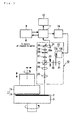
- Figure 1 is a schematic structural diagram which shows a polishing apparatus constituting a first working configuration of the present invention in model form.
- This polishing apparatus is equipped with a polishing member 1, an object of polishing holding part 3 (hereafter referred to as a "wafer holder") which holds (for example) a process wafer 2 having Cu as the object of polishing on the lower side of the polishing member 1, and a polishing agent supply part (not shown in the figures) which supplies a polishing agent (slurry) to the surface of the wafer 2.
- a polishing member 1 an object of polishing holding part 3 (hereafter referred to as a "wafer holder") which holds (for example) a process wafer 2 having Cu as the object of polishing on the lower side of the polishing member 1, and a polishing agent supply part (not shown in the figures) which supplies a polishing agent (slurry) to the surface of the wafer 2.
- the polishing member 1 has a polishing body (polishing pad) 6 disposed on the undersurface of a polishing platen 5, and can be caused to rotate (as indicated by the arrow in Figure 1), move upward and downward and swing to the left and right (reciprocating motion) by a mechanism not shown in the figures.
- a sheet-form foam polyurethane or a non-foam resin which has a groove structure in the surface can be used as the polishing body 6.
- the wafer 2 is held on the wafer holder 3, and the upper surface of the wafer 2 is the polished surface.
- the wafer holder 3 can be caused to rotate as indicated by the arrow in Figure 1 by a mechanism (not shown in the figures) using an electric motor as an actuator.
- the diameter of the polishing member 1 is set so that this diameter is smaller than the diameter of the wafer 2; thus the footprint of the apparatus as a whole is small.
- a portion of the wafer 2 can be temporarily exposed from the polishing member 1 by swinging the polishing member 1 during polishing.
- a window for illuminating the wafer 2 with the measuring light may be formed in the polishing member 1 in a universally known manner.
- the polishing member 1 is pressed against the upper surface of the wafer 2 on the wafer holder 3 by a specified pressure while the polishing member 1 rotates and swings.
- the wafer holder 3 is caused to rotate so that the wafer 2 is also caused to rotate, thus causing a relative movement to be performed between the wafer 2 and the polishing member 1.
- a polishing agent is supplied to the surface of the wafer 2 from a polishing agent supply part. This polishing agent diffuses over the surface of the wafer 2, and enters the space between the polishing body 6 and the wafer 2 as relative movement takes place between the polishing member 1 and the wafer 2, so that the polished surface of the wafer 2 is polished.
- this polishing apparatus has a polishing control part 9 which controls the motors of the respective parts that cause rotation and swinging, etc., of the polishing member 1 and rotation of the wafer holder 3.
- this polishing apparatus is also equipped with a measurement optical system 10 which constitutes a polishing state monitoring device, a signal processing part 11 which consists of a personal computer, etc., a display part 12 such as a CRT which displays the monitoring results, and a shutter mechanism control part 14 which controls a shutter mechanism 13 installed in the measurement optical system 10.
- a measurement optical system 10 which constitutes a polishing state monitoring device
- a signal processing part 11 which consists of a personal computer, etc.
- a display part 12 such as a CRT which displays the monitoring results
- a shutter mechanism control part 14 which controls a shutter mechanism 13 installed in the measurement optical system 10.
- the measurement optical system 10 illuminates the portion of the polished surface (upper surface) of the wafer 2 that is exposed from the polishing member 1 (hereafter referred to as the "exposed portion") with measuring light, and obtains a detection signal that relates to the reflected light received by a light receiving sensor that receives the light reflected by the polished surface of the wafer 2.
- This detection signal is input into the signal processing part 112 as a monitoring signal.
- the signal processing part 11 performs processing that monitors the polishing state.
- the signal processing part 11 causes the polishing state to be displayed by the display part 12, ascertains the polishing endpoint, and respectively sends a polishing endpoint detection signal to the polishing control part 9 and shutter mechanism control part 14 when the polishing endpoint is detected.
- the polishing control part 9 ends the polishing operation in response to this polishing endpoint detection signal.
- 21 indicates a white light source which has multiple wavelength components; for example, a white LED, xenon lamp or halogen lamp can be used as this light source.
- light from the light source 21 can be conducted by an optical fiber. If the light blocking member 13a of the shutter mechanism 13 (described later) is withdrawn from the light path, the light from the light source 21 is converted into a parallel light beam by a lens 22, and then passes through a visual field diaphragm 23, after which the light is caused to be incident on a beam splitter 24. The direction of this light is altered 90° by the beam splitter 24; the light then passes through relay lenses 25 and 26, and is again converted into a parallel light beam and directed onto the exposed portion of the polished surface of the wafer 2 as measuring light.
- the light reflected from the wafer 2 again passes through the relay lenses 26 and 25, and is caused to be incident on the beam splitter 24 as a parallel light beam.
- This light passes through the beam splitter 24, and is focused on the pinhole (this may also be a slit) 28a of a light blocking plate 28 by a lens 27.
- noise components such as scattered light and diffracted light are removed by the light blocking plate 28, and the light passing through the pinhole 28a (regular reflected light (zero-order light)) is projected via a lens 29 onto a diffraction grating (this may also be some other spectroscopic device such as a spectroscopic prism) 30 that is used as a spectroscopic device, so that the light is separated into a spectrum.
- the light that has been separated into a spectrum enters a linear sensor 31 used as a light receiving sensor, and the spectroscopic intensity (intensity at respective wavelengths, i.e., spectrum) is measured.
- the signal processing part 11 calculates the polishing state monitoring results for the wafer 2 on the basis of the spectroscopic intensity obtained from the linear sensor 31, causes these results to be displayed on the display part 12, ascertains the polishing endpoint, and respectively sends a polishing endpoint detection signal to the polishing control part 9 and shutter mechanism control part 14 when the polishing endpoint is detected.
- the film thickness of the layer that is being polished is calculated from characteristic quantities such as the positions (wavelength) of maxima and minima of the waveform of the spectroscopic intensity (corresponding to the spectroscopic reflectivity), and this film thickness is displayed on the display part 12 as the results of monitoring; furthermore, the polishing endpoint is detected according to whether or not this film thickness has reached a specified film thickness.
- the amount of polishing is determined from the initial thickness of the wafer 2 and the film thickness of the layer that is being polished (uppermost layer), and this value is displayed on the display part 12 as the results of monitoring.
- the calculation method used to determine the monitoring results from the spectroscopic intensity and the method used to detect the polishing endpoint are not limited to the examples described above; for example, other methods such as those disclosed in Japanese Patent Application Kokai No. H10-335288 and Japanese Patent Application Kokai No. H11-33901 may also be used.
- the measurement optical system 10 performs spectroscopic reflection measurements, and the signal processing part 11 monitors the polishing state on the basis of the spectroscopic reflection intensity.
- the present invention is not limited to such an arrangement; for example, it would also be possible to construct the device of the present invention so that the measurement optical system 10 performs measurements of reflected light that do not depend on spectroscopy (e.g., measurements of the reflectivity of light at a specified wavelength), and so that the polishing endpoint is detected on the basis of the reflectivity measured by the measurement optical system 10. This is also true of the respective working configurations described later.
- a mechanical shutter mechanism 13 is installed in the measurement optical system 10.
- the shutter mechanism 13 is constructed from a light blocking member 13a, and a motor 13b such as a stepping motor as a moving mechanism that causes the light blocking member 13a to advance into and withdraw from the light path between the light source 21 and the lens 22 (this mechanism may be installed at any location in the light path between the light source 21 and the wafer 2).
- this mechanism may be installed at any location in the light path between the light source 21 and the wafer 2).
- the light source 21 is driven so that the light source is continuously lit with a fixed quantity of light when the power supply is switched on.
- the shutter mechanism control part 14 controls the motor 13b so that the light blocking member 13a is withdrawn from the light path.
- the monitoring start command may be issued at the time that the polishing of the wafer 2 is initiated, or may be issued after a specified period of time has elapsed following the initiation of the polishing of the wafer 2.
- the shutter mechanism control part 14 controls the motor 13b so that the light blocking member 13a advances into the light path.
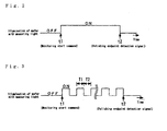
- the wafer 2 is illuminated with measuring light only during the period extending from the point in time t1 at which the monitoring start command is received to the point in time t2 at which the polishing endpoint detection signal is received.
- the shutter mechanism 13 and shutter mechanism control part 14 constitute a first measuring light control part which blocks the measuring light (or reduces the measuring light in cases where a light reducing filter is used instead of the light blocking member 13a) with respect to the wafer 2 in response to the polishing endpoint detection signaL
- the measuring light used to monitor the polishing state is blocked or reduced with respect to the wafer 2 after the polishing endpoint of the wafer 2 has been detected. Accordingly, the effect of the measuring light used to monitor the polishing state on the wafer 2 can be reduced or eliminated.
- the wafer 2 is continuously illuminated with a fixed quantity of measuring light during the monitoring of the polishing state (i.e., during the time period extending from the point in time t1 at which the monitoring start command is received to the point in time t2 at which the polishing endpoint detection signal is received).
- the system may also be arranged so that a first period T1 during which the wafer 2 is illuminated with the measuring light, and a second period T2 during which the measuring light is blocked (or reduced) with respect to the wafer 2, are repeated during the monitoring of the polishing state as shown in Figure 3.
- the system may be devised as follows: specifically, in response to a monitoring start command, the shutter mechanism control part 14 continues to cause the motor 13b to rotate continuously (here, the measuring light is chopped by the light blocking member 13a), and in response to the polishing endpoint detection signal, the shutter mechanism control part 14 stops the motor 13a so that the light blocking member 13a stops in a position in which this member has advanced into the light path.
- the system may be devised so that (for example) a position detector such as an encoder which detects the rotational position of the motor 13a is installed, detection of the light that is incident on the linear sensor 31 during the period T1 in which the light is not blocked by the light blocking member 13a is performed in synchronization with signals from the above-mentioned position detector, and data input of the light detection signal and calculations such as film thickness calculations and endpoint determination based on this data input are performed during the period T2 in which the light is blocked by the light blocking member 13a.
- a position detector such as an encoder which detects the rotational position of the motor 13a is installed
- detection of the light that is incident on the linear sensor 31 during the period T1 in which the light is not blocked by the light blocking member 13a is performed in synchronization with signals from the above-mentioned position detector
- data input of the light detection signal and calculations such as film thickness calculations and endpoint determination based on this data input are performed during the period T2 in which the light is blocked by the light blocking member 13
- the shutter mechanism 13 and shutter mechanism control part 14 also function as a second measuring light control part which causes a first period T1 during which the wafer 2 is illuminated with the measuring light, and a second period T2 during which the measuring light is blocked (or reduced) with respect to the wafer 2, to be repeated during the monitoring of the polishing state.
- Figure 4 is a schematic structural diagram which shows a polishing apparatus constituting a second working configuration of the present invention in model form.
- elements that are the same as in Figure 1, or that correspond to elements in Figure 1 are labeled with the same symbols, and a redundant description is omitted.
- the present working configuration differs from the above-mentioned first working configuration only in that a light source control part 34 is used instead of the shutter mechanism 13 and shutter mechanism control part 14.
- a light source which causes no problems in terms of useful life or response characteristics when switched on and off by electrical control e.g., a white LED, is used as the light source 21.
- the light source control part 34 electrically controls the light-emitting state of the light source 21 so that an illumination pattern of the measuring light with respect to the wafer 2 such as that shown in Figure 2 (which is similar to the above-mentioned first working configuration) is realized.
- the light source control part 34 may electrically control the light-emitting state of the light source 21 so that an illumination pattern of the measuring light with respect to the wafer 2 such as that shown in the above-mentioned Figure 3 is realized. Furthermore, it would also be possible to devise the system so that the emission of light by the light source 21 is not completely stopped in the OFF periods in Figures 2 and 3, but is instead reduced (reduced-light state).
- Figure 5 is a schematic structural diagram which shows a polishing apparatus constituting a third working configuration of the present invention in model form.
- elements that are the same as in Figure 1, or that correspond to elements in Figure 1 are labeled with the same symbols, and a redundant description is omitted.
- the present working configuration differs from the above-mentioned first working configuration.
- the shutter mechanism 13 and shutter mechanism control part 14 shown in Figure 1 are removed.
- a reference mirror 42 which has specified reflection characteristics and which is used to acquire a reference signal
- a motor 43 which is used as a moving mechanism that causes the reference mirror 42 to advance into and withdraw from the light path of the measuring light at a point closest to the wafer 2 among the positions of all of the optical elements, etc.
- a dark noise measuring member 44 which absorbs light more or less completely and which is used to measure dark noise
- a motor 45 which is used as a moving mechanism that causes the dark noise measuring member 44 to advance into and withdraw from the light path of the measuring light at a point closest to the wafer 2 among the positions of all of the optical elements, etc.
- a control part 41 which controls the motors 43 and 45, are added.
- the control part 41 receives a reference signal acquisition start command (ordinarily issued with an appropriate timing other than during the polishing of the wafer 2) from the polishing control part 9 via the signal processing part 11; in response to this command, the control part 41 controls the motor 43 so that the reference mirror 42 advances into the light path.
- the signal processing part 11 inputs a signal from the linear sensor 31 as a reference signal.
- This reference signal is used as a reference for comparison with the measurement signal from the linear sensor 31 that is obtained by illuminating the wafer 2 with the measuring light during the monitoring of the polishing state; the above-mentioned calculation of the film thickness, etc., is performed on the basis of this comparison.
- the control part 41 controls the motor 43 so that the reference mirror 42 is withdrawn from the light path.
- the control part 41 receives a dark noise measurement start command (ordinarily issued with an appropriate timing other than during the polishing of the wafer 2) from the polishing control part 9 via the signal processing part 11; in response to this command, the control part 41 controls the motor 45 so that the dark noise measuring member 44 advances into the light path.
- the signal processing part 11 inputs a signal from the linear sensor 31 as a dark noise measurement signal.
- This measurement signal is used to subtract the dark noise component from the measurement signal of the linear sensor 31 that is obtained by illuminating the wafer 2 with measuring light during the monitoring of the polishing state; the calculation of the above-mentioned film thickness, etc., is performed on the basis of the signal obtained by this subtraction. Then, in response to a dark noise measurement end command issued from the signal processing part 11 when the measurement of dark noise is ended, the control part 41 controls the motor 45 so that the dark noise measuring member 44 is withdrawn from the light path.
- the acquisition of a reference signal and the measurement of dark noise can be accomplished by respectively causing the reference mirror 42 and dark noise measuring member 44 to advance into and withdraw from the light path of the measuring light by means of the motors 43 and 45. Accordingly, in the present working configuration, the acquisition of a reference signal and the measurement of dark noise can be performed in parallel with the conveying of the wafer 2 to and from the polishing position, so that the polishing throughput is improved. Furthermore, in the present working configuration, the acquisition of a reference signal and the measurement of dark noise can be frequently performed while improving the polishing throughput; accordingly, the polishing state of the wafer 2 can be monitored on the basis of the most recent reference signal or dark noise, and the precision of the monitoring of the polishing state can therefore be improved.
- the wafer 2 could also be constantly illuminated with a fixed quantity of light both during the monitoring of the polishing state and after polishing is completed.
- the control part 41 may be constructed so that this control part 41 performs a control action similar to that of the shutter mechanism control part 14 in Figure 1.
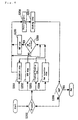
- FIG. 6 is a flow chart which illustrates a semiconductor device manufacturing process.
- the appropriate treatment step is first selected in step S200 from the steps S201 through S204 described below. The processing then proceeds to one of the steps S201 through S204 in accordance with this selection.
- Step S201 is an oxidation step in which the surface of the silicon wafer is oxidized.
- Step S202 is a CVD step in which an insulating film is formed on the surface of the silicon wafer by CVD, etc.
- Step S203 is an electrode formation step in which an electrode film is formed on the silicon wafer by vacuum evaporation, etc.
- Step S204 is an ion injection step in which ions are injected into the silicon wafer.
- Step S209 a judgement is made as to whether or not a CMP step is to be performed. In cases where such a step is not to be performed, the processing proceeds to step S206, while in cases where such a step is to be performed, the processing proceeds to step S205.
- Step S205 is a CMP step; in this step, the flattening of inter-layer insulating films or the formation of a damascene by polishing a metal film (Cu film, etc.) on the surface of a semiconductor device is performed using the polishing apparatus of the present invention.
- Step S206 is a photolithographic step.
- the silicon wafer is coated with a resist, circuit patterns are burned onto the silicon wafer by exposure using an exposure apparatus, and the exposed silicon wafer is developed.
- the next step S207 is an etching step in which the portions other than the developed resist image are removed by etching, the resist is then peeled away, and the resist that has become unnecessary following etching is removed.
- step S208 a judgement is made as to whether or not all of the necessary steps have been completed. If these steps have not bee been completed, the processing returns to step S200, and the subsequent steps are repeated, so that circuit patterns are formed on the silicon wafer. If it is judged in step S208 that all of the steps have been completed, the process is ended.
- the polishing apparatus of the present invention is used in the CMP step. Accordingly, the danger of problems such as oxidation of the Cu film, etc., caused by the measuring light used to monitor the polishing state is reduced or eliminated, so that the yield can be improved.
- the following advantage is obtained: namely, semiconductor devices can be manufactured at a lower cost than in conventional semiconductor device manufacturing methods.
- the following advantage is also obtained instead of or in addition to the above-mentioned advantage: namely, the polishing throughput can be improved, so that semiconductor devices can be manufactured at a lower cost than in conventional semiconductor device manufacturing methods.
- the present invention has the effect of achieving the manufacture of semiconductor devices at a lower cost than in conventional semiconductor device manufacturing methods.
- polishing apparatus of the present invention may also be used in the CMP steps of semiconductor device manufacturing processes other than the semiconductor device manufacturing process described above.
- the semiconductor device of the present invention is manufactured by the semiconductor device manufacturing method of the present invention. As a result, this semiconductor device can be manufactured at a lower cost than in conventional semiconductor device manufacturing methods, which has the effect of reducing the manufacturing cost of the semiconductor device.
- the present invention can be used (for example) to manufacture semiconductor devices and to polish wafers in the manufacturing process of such semiconductor devices.
Landscapes
- Engineering & Computer Science (AREA)
- Mechanical Engineering (AREA)
- Mechanical Treatment Of Semiconductor (AREA)
- Constituent Portions Of Griding Lathes, Driving, Sensing And Control (AREA)
- Finish Polishing, Edge Sharpening, And Grinding By Specific Grinding Devices (AREA)
- Length Measuring Devices By Optical Means (AREA)
- Testing Or Measuring Of Semiconductors Or The Like (AREA)
Abstract
Description
Claims (16)
- A polishing state monitoring method in which the object of polishing is illuminated with measuring light, and the polishing state of the above-mentioned object of polishing is monitored during the polishing of this object of polishing on the basis of the light obtained from the above-mentioned object of polishing as a result of illumination with the above-mentioned measuring light, wherein the above-mentioned measuring light is blocked or reduced with respect to the above-mentioned object of polishing after the polishing endpoint of the above-mentioned object of polishing has been detected.
- The polishing state monitoring method according to Claim 1, wherein a first period during which the above-mentioned object of polishing is illuminated with the above-mentioned measuring light, and a second period during which the above-mentioned measuring light is blocked or reduced with respect to the above-mentioned object of polishing, are repeated during the monitoring of the above-mentioned polishing state.
- A polishing state monitoring method in which the object of polishing is illuminated with measuring light, and the polishing state of the above-mentioned object of polishing is monitored during the polishing of this object of polishing on the basis of the light obtained from the above-mentioned object of polishing as a result of illumination with the above-mentioned measuring light, wherein a first period during which the above-mentioned object of polishing is illuminated with the above-mentioned measuring light, and a second period during which the above-mentioned measuring light is blocked or reduced with respect to the above-mentioned object of polishing, are repeated during the monitoring of the above-mentioned polishing state.
- A polishing state monitoring device in which the above-mentioned object of polishing is illuminated with measuring light, and the polishing state is monitored on the basis of the light that is obtained from the above-mentioned object of polishing as a result of illumination with the above-mentioned measuring light, wherein the device is equipped with a first measuring light control part that blocks or reduces the above-mentioned measuring light with respect to the above-mentioned object of polishing in response to a polishing endpoint detection signal.
- The polishing state monitoring device according to Claim 4, wherein the above-mentioned first measuring light control part includes a control part that electrically controls the light-emitting state of the above-mentioned light source.
- The polishing state monitoring device according to Claim 4, wherein the above-mentioned first measuring light control part includes a mechanical shutter mechanism.
- The polishing state monitoring device according to Claim 6, wherein the above-mentioned shutter mechanism includes a reference mirror that is used to obtain a reference signal as a light blocking member.
- The polishing state monitoring device according to Claim 6, wherein the above-mentioned shutter mechanism includes a dark noise measuring member (used to measure dark noise) as a light blocking member.
- The polishing state monitoring device according to any of Claims 4 through 8, wherein the device is equipped with a second measuring light control part which causes a first period during which the above-mentioned object of polishing is illuminated with the above-mentioned measuring light, and a second period during which the above-mentioned measuring light is blocked or reduced with respect to the above-mentioned object of polishing, to be repeated during the monitoring of the above-mentioned polishing state.
- The polishing state monitoring device according to Claim 9, wherein at least a portion of the above-mentioned first measuring light control part and at least a portion of the above-mentioned second measuring light control part are used in common.
- A polishing state monitoring device in which the object of polishing is illuminated with measuring light, and the polishing state is monitored on the basis of the light obtained from the above-mentioned object of polishing as a result of this illumination with the above-mentioned measuring light, wherein the device is equipped with a measuring light control part which causes a first period during which the above-mentioned object of polishing is illuminated with the above-mentioned measuring light, and a second period during which the above-mentioned measuring light is blocked or reduced with respect to the above-mentioned object of polishing, to be repeated during the monitoring of the above-mentioned polishing state.
- A polishing state monitoring device in which the object of polishing is illuminated with measuring light, and the polishing state is monitored on the basis of the light obtained from the above-mentioned object of polishing as a result of this illumination with the above-mentioned measuring light, wherein the device is equipped with a reference mirror which is used to obtain a reference signal, and a moving mechanism which causes the above·mentioned reference mirror to advance into and withdraw from the light path of the above-mentioned measuring light.
- A polishing state monitoring device in which the object of polishing is illuminated with measuring light, and the polishing state is monitored on the basis of the light obtained from the above-mentioned object of polishing as a result of this illumination with the above-mentioned measuring light, wherein the device is equipped with a dark noise measuring member that is used to measure dark noise, and a moving mechanism which causes the above-mentioned dark noise measuring member to advance into and withdraw from the light path of the above-mentioned measuring light.
- A polishing apparatus which is equipped with a polishing body and a holding part that holds the object of polishing, and in which the above-mentioned object of polishing is polished by applying a load between the above-mentioned polishing body and the above-mentioned object of polishing, and causing relative movement between the above-mentioned polishing body and the above-mentioned object of polishing, in a state in which a polishing agent is interposed between the above-mentioned polishing body and the above-mentioned object of polishing, wherein the apparatus is equipped with the polishing state monitoring device according to any of Claims 4 through 13.
- A semiconductor device manufacturing method which is characterized by the fact that this method has a process in which the surfaces of semiconductor wafers are flattened using the polishing apparatus according to Claim 14.
- A semiconductor device which is characterized by the fact that this device is manufactured by the semiconductor device manufacturing method according to Claim 15.
Applications Claiming Priority (3)
| Application Number | Priority Date | Filing Date | Title |
|---|---|---|---|
| JP2000367876 | 2000-12-04 | ||
| JP2000367876A JP4810728B2 (en) | 2000-12-04 | 2000-12-04 | Polishing condition monitoring method and apparatus, polishing apparatus, and semiconductor device manufacturing method |
| PCT/JP2001/009736 WO2002047141A1 (en) | 2000-12-04 | 2001-11-07 | Polishing progress monitoring method and device thereof, polishing device, semiconductor device production method, and semiconductor device |
Publications (3)
| Publication Number | Publication Date |
|---|---|
| EP1341223A1 true EP1341223A1 (en) | 2003-09-03 |
| EP1341223A4 EP1341223A4 (en) | 2005-06-08 |
| EP1341223B1 EP1341223B1 (en) | 2006-08-16 |
Family
ID=18838223
Family Applications (1)
| Application Number | Title | Priority Date | Filing Date |
|---|---|---|---|
| EP01981005A Expired - Lifetime EP1341223B1 (en) | 2000-12-04 | 2001-11-07 | Polishing progress monitoring device and polishing device |
Country Status (8)
| Country | Link |
|---|---|
| US (1) | US7481945B2 (en) |
| EP (1) | EP1341223B1 (en) |
| JP (1) | JP4810728B2 (en) |
| KR (1) | KR100834425B1 (en) |
| CN (1) | CN1208812C (en) |
| DE (1) | DE60122371T2 (en) |
| TW (1) | TW531471B (en) |
| WO (1) | WO2002047141A1 (en) |
Cited By (2)
| Publication number | Priority date | Publication date | Assignee | Title |
|---|---|---|---|---|
| WO2004043647A1 (en) * | 2002-11-08 | 2004-05-27 | Freescale Semiconductor, Inc. | Apparatus for and method of wafer grinding |
| WO2008027680A1 (en) * | 2006-08-28 | 2008-03-06 | Micron Technology, Inc. | Methods and tools for controlling the removal of material from microfeature workpieces |
Families Citing this family (17)
| Publication number | Priority date | Publication date | Assignee | Title |
|---|---|---|---|---|
| US7078344B2 (en) * | 2003-03-14 | 2006-07-18 | Lam Research Corporation | Stress free etch processing in combination with a dynamic liquid meniscus |
| JP4464642B2 (en) * | 2003-09-10 | 2010-05-19 | 株式会社荏原製作所 | Polishing state monitoring apparatus, polishing state monitoring method, polishing apparatus, and polishing method |
| KR101357290B1 (en) * | 2006-10-06 | 2014-01-28 | 가부시끼가이샤 도시바 | Processing end point detection method, polishing method, and polishing apparatus |
| JP5037974B2 (en) * | 2007-03-14 | 2012-10-03 | 株式会社岡本工作機械製作所 | Monitoring device and monitoring method for semiconductor substrate in polishing stage |
| JP2009129970A (en) * | 2007-11-20 | 2009-06-11 | Ebara Corp | Polishing apparatus and polishing method |
| US8579675B2 (en) | 2008-11-26 | 2013-11-12 | Applied Materials, Inc. | Methods of using optical metrology for feed back and feed forward process control |
| CN102136441B (en) * | 2010-01-26 | 2012-09-26 | 中芯国际集成电路制造(上海)有限公司 | Method for detecting chemical mechanical lapping terminal point |
| SG188414A1 (en) | 2010-11-12 | 2013-04-30 | Ev Group E Thallner Gmbh | Measurement means and method for measuring layer thicknesses and voids of a wafer stack |
| CN105737773B (en) * | 2010-11-12 | 2019-04-19 | Ev 集团 E·索尔纳有限责任公司 | Measurement device and method for measuring layer thickness and lattice defects of wafer stacks |
| US8535115B2 (en) * | 2011-01-28 | 2013-09-17 | Applied Materials, Inc. | Gathering spectra from multiple optical heads |
| US9393669B2 (en) * | 2011-10-21 | 2016-07-19 | Strasbaugh | Systems and methods of processing substrates |
| US9610669B2 (en) | 2012-10-01 | 2017-04-04 | Strasbaugh | Methods and systems for use in grind spindle alignment |
| US9457446B2 (en) | 2012-10-01 | 2016-10-04 | Strasbaugh | Methods and systems for use in grind shape control adaptation |
| CN110125793B (en) * | 2016-12-23 | 2021-02-26 | 浙江大学台州研究院 | Quartz wafer measurement and control method based on automatic resonant frequency search mechanism |
| CN107180751A (en) * | 2017-04-14 | 2017-09-19 | 天津华海清科机电科技有限公司 | Handle the control method of crystal column surface |
| CN111390698B (en) * | 2020-06-03 | 2020-09-01 | 宁波丞达精机有限公司 | Optical lens edging device and edging method |
| CN114029790B (en) * | 2021-11-25 | 2023-04-07 | 北京晶亦精微科技股份有限公司 | Wafer grinding method |
Family Cites Families (17)
| Publication number | Priority date | Publication date | Assignee | Title |
|---|---|---|---|---|
| US5433651A (en) * | 1993-12-22 | 1995-07-18 | International Business Machines Corporation | In-situ endpoint detection and process monitoring method and apparatus for chemical-mechanical polishing |
| JPH10229060A (en) * | 1997-02-13 | 1998-08-25 | Nikon Corp | Polishing amount measuring device |
| US6111634A (en) * | 1997-05-28 | 2000-08-29 | Lam Research Corporation | Method and apparatus for in-situ monitoring of thickness using a multi-wavelength spectrometer during chemical-mechanical polishing |
| JPH10335288A (en) | 1997-06-05 | 1998-12-18 | Sony Corp | Substrate polishing apparatus and polishing end point detection method |
| US6489624B1 (en) * | 1997-07-18 | 2002-12-03 | Nikon Corporation | Apparatus and methods for detecting thickness of a patterned layer |
| JP3327175B2 (en) | 1997-07-18 | 2002-09-24 | 株式会社ニコン | Detection unit and wafer polishing apparatus provided with the detection unit |
| US6142855A (en) * | 1997-10-31 | 2000-11-07 | Canon Kabushiki Kaisha | Polishing apparatus and polishing method |
| JPH11198033A (en) * | 1997-10-31 | 1999-07-27 | Canon Inc | Polishing apparatus and polishing method |
| JPH11251317A (en) * | 1998-03-04 | 1999-09-17 | Hitachi Ltd | Semiconductor device manufacturing method and manufacturing apparatus |
| US6271047B1 (en) * | 1998-05-21 | 2001-08-07 | Nikon Corporation | Layer-thickness detection methods and apparatus for wafers and the like, and polishing apparatus comprising same |
| US6361646B1 (en) * | 1998-06-08 | 2002-03-26 | Speedfam-Ipec Corporation | Method and apparatus for endpoint detection for chemical mechanical polishing |
| JP3141939B2 (en) * | 1998-11-26 | 2001-03-07 | 日本電気株式会社 | Metal wiring formation method |
| JP2000183002A (en) * | 1998-12-10 | 2000-06-30 | Okamoto Machine Tool Works Ltd | Wafer polishing end point detecting method and polishing end point detecting apparatus |
| JP2000183000A (en) * | 1998-12-14 | 2000-06-30 | Fujitsu Ltd | Semiconductor device manufacturing method, manufacturing apparatus, and inspection apparatus |
| JP2000315666A (en) * | 1999-04-28 | 2000-11-14 | Hitachi Ltd | Method for manufacturing semiconductor integrated circuit device |
| JP2000317826A (en) * | 1999-05-07 | 2000-11-21 | Okamoto Machine Tool Works Ltd | Substrate polishing end point detection method and polishing end point detection device |
| US6540587B1 (en) * | 2000-10-13 | 2003-04-01 | Lam Research Corporation | Infrared end-point detection system |
-
2000
- 2000-12-04 JP JP2000367876A patent/JP4810728B2/en not_active Expired - Fee Related
-
2001
- 2001-11-07 KR KR1020037005766A patent/KR100834425B1/en not_active Expired - Lifetime
- 2001-11-07 WO PCT/JP2001/009736 patent/WO2002047141A1/en not_active Ceased
- 2001-11-07 CN CNB018178979A patent/CN1208812C/en not_active Expired - Lifetime
- 2001-11-07 EP EP01981005A patent/EP1341223B1/en not_active Expired - Lifetime
- 2001-11-07 US US10/433,395 patent/US7481945B2/en not_active Expired - Lifetime
- 2001-11-07 DE DE60122371T patent/DE60122371T2/en not_active Expired - Lifetime
- 2001-12-04 TW TW090129901A patent/TW531471B/en not_active IP Right Cessation
Cited By (4)
| Publication number | Priority date | Publication date | Assignee | Title |
|---|---|---|---|---|
| WO2004043647A1 (en) * | 2002-11-08 | 2004-05-27 | Freescale Semiconductor, Inc. | Apparatus for and method of wafer grinding |
| WO2008027680A1 (en) * | 2006-08-28 | 2008-03-06 | Micron Technology, Inc. | Methods and tools for controlling the removal of material from microfeature workpieces |
| US7527545B2 (en) | 2006-08-28 | 2009-05-05 | Micron Technology, Inc. | Methods and tools for controlling the removal of material from microfeature workpieces |
| US7988529B2 (en) | 2006-08-28 | 2011-08-02 | Micron Technology, Inc. | Methods and tools for controlling the removal of material from microfeature workpieces |
Also Published As
| Publication number | Publication date |
|---|---|
| TW531471B (en) | 2003-05-11 |
| DE60122371D1 (en) | 2006-09-28 |
| EP1341223B1 (en) | 2006-08-16 |
| JP2002166360A (en) | 2002-06-11 |
| JP4810728B2 (en) | 2011-11-09 |
| WO2002047141A1 (en) | 2002-06-13 |
| EP1341223A4 (en) | 2005-06-08 |
| DE60122371T2 (en) | 2007-09-13 |
| CN1471725A (en) | 2004-01-28 |
| KR100834425B1 (en) | 2008-06-04 |
| US7481945B2 (en) | 2009-01-27 |
| KR20030059214A (en) | 2003-07-07 |
| US20040053500A1 (en) | 2004-03-18 |
| CN1208812C (en) | 2005-06-29 |
Similar Documents
| Publication | Publication Date | Title |
|---|---|---|
| US7481945B2 (en) | Polishing progress monitoring method and device thereof, polishing device, semiconductor device production method, and semiconductor device | |
| KR101011051B1 (en) | Method and apparatus for generating a library of spectra and high yield measurement system | |
| US6334807B1 (en) | Chemical mechanical polishing in-situ end point system | |
| KR101715726B1 (en) | Using optical metrology for feed back and feed forward process control | |
| US10948900B2 (en) | Display of spectra contour plots versus time for semiconductor processing system control | |
| US6307628B1 (en) | Method and apparatus for CMP end point detection using confocal optics | |
| JP5542802B2 (en) | Endpoint detection in chemical mechanical polishing using multiple spectra | |
| KR101504508B1 (en) | Use of spectra to determine polishing end points | |
| KR100465929B1 (en) | Method and apparatus for monitoring polishing state, polishing device, process wafer, semiconductor device, and method of manufacturing semiconductor device | |
| TWI465314B (en) | Establish a reference spectrum with environmental effect variation | |
| US20010003084A1 (en) | Method and system for endpoint detection | |
| US20050026542A1 (en) | Detection system for chemical-mechanical planarization tool | |
| KR19980019169A (en) | Polishing Method and Polishing Device (POLISHING METHOD APPARATUS) | |
| KR101361875B1 (en) | Method for detecting polishing end in cmp polishing device, cmp polishing device, and semiconductor device manufacturing method | |
| TW202035069A (en) | Polishing method and polishing apparatus | |
| WO2004090502A2 (en) | Whole-substrate spectral imaging system for cmp | |
| JP5376293B2 (en) | End point detection device and polishing device | |
| JP2000077371A (en) | Detection method, detection device, and polishing device | |
| JP2006032764A (en) | Polishing control method, polishing apparatus, and semiconductor device manufacturing method | |
| JP2003168666A (en) | Film layer state measuring method, film layer state measuring device, polishing apparatus, and semiconductor device manufacturing method | |
| KR20030024920A (en) | Method and apparatus for measuring a polishing condition | |
| JP2005322939A (en) | Wafer polishing method | |
| JP3681953B2 (en) | Film thickness measuring method and film thickness measuring apparatus | |
| WO2025072007A1 (en) | Finding substrate notch on substrate between platens in chemical mechanical polishing | |
| JP2001260016A (en) | Polishing state measuring apparatus and measuring method, polishing apparatus and semiconductor device manufacturing method |
Legal Events
| Date | Code | Title | Description |
|---|---|---|---|
| PUAI | Public reference made under article 153(3) epc to a published international application that has entered the european phase |
Free format text: ORIGINAL CODE: 0009012 |
|
| 17P | Request for examination filed |
Effective date: 20030603 |
|
| AK | Designated contracting states |
Kind code of ref document: A1 Designated state(s): AT BE CH CY DE DK ES FI FR GB GR IE IT LI LU MC NL PT SE TR |
|
| RBV | Designated contracting states (corrected) |
Designated state(s): AT BE CH CY DE FR GB LI NL |
|
| A4 | Supplementary search report drawn up and despatched |
Effective date: 20050426 |
|
| RIC1 | Information provided on ipc code assigned before grant |
Ipc: 7B 24B 49/04 B Ipc: 7B 24B 49/12 B Ipc: 7H 01L 21/304 B Ipc: 7H 01L 21/306 B Ipc: 7B 24B 37/04 A |
|
| GRAP | Despatch of communication of intention to grant a patent |
Free format text: ORIGINAL CODE: EPIDOSNIGR1 |
|
| RBV | Designated contracting states (corrected) |
Designated state(s): DE FR GB NL |
|
| RTI1 | Title (correction) |
Free format text: POLISHING PROGRESS MONITORING DEVICE AND POLISHING DEVICE |
|
| GRAS | Grant fee paid |
Free format text: ORIGINAL CODE: EPIDOSNIGR3 |
|
| GRAA | (expected) grant |
Free format text: ORIGINAL CODE: 0009210 |
|
| AK | Designated contracting states |
Kind code of ref document: B1 Designated state(s): DE FR GB NL |
|
| REG | Reference to a national code |
Ref country code: GB Ref legal event code: FG4D |
|
| REF | Corresponds to: |
Ref document number: 60122371 Country of ref document: DE Date of ref document: 20060928 Kind code of ref document: P |
|
| NLR4 | Nl: receipt of corrected translation in the netherlands language at the initiative of the proprietor of the patent | ||
| ET | Fr: translation filed | ||
| PLBE | No opposition filed within time limit |
Free format text: ORIGINAL CODE: 0009261 |
|
| STAA | Information on the status of an ep patent application or granted ep patent |
Free format text: STATUS: NO OPPOSITION FILED WITHIN TIME LIMIT |
|
| 26N | No opposition filed |
Effective date: 20070518 |
|
| PGFP | Annual fee paid to national office [announced via postgrant information from national office to epo] |
Ref country code: NL Payment date: 20091114 Year of fee payment: 9 |
|
| PGFP | Annual fee paid to national office [announced via postgrant information from national office to epo] |
Ref country code: GB Payment date: 20091104 Year of fee payment: 9 |
|
| REG | Reference to a national code |
Ref country code: NL Ref legal event code: V1 Effective date: 20110601 |
|
| GBPC | Gb: european patent ceased through non-payment of renewal fee |
Effective date: 20101107 |
|
| PG25 | Lapsed in a contracting state [announced via postgrant information from national office to epo] |
Ref country code: NL Free format text: LAPSE BECAUSE OF NON-PAYMENT OF DUE FEES Effective date: 20110601 |
|
| PG25 | Lapsed in a contracting state [announced via postgrant information from national office to epo] |
Ref country code: GB Free format text: LAPSE BECAUSE OF NON-PAYMENT OF DUE FEES Effective date: 20101107 |
|
| REG | Reference to a national code |
Ref country code: FR Ref legal event code: PLFP Year of fee payment: 15 |
|
| REG | Reference to a national code |
Ref country code: FR Ref legal event code: PLFP Year of fee payment: 16 |
|
| REG | Reference to a national code |
Ref country code: FR Ref legal event code: PLFP Year of fee payment: 17 |
|
| REG | Reference to a national code |
Ref country code: FR Ref legal event code: PLFP Year of fee payment: 18 |
|
| PGFP | Annual fee paid to national office [announced via postgrant information from national office to epo] |
Ref country code: DE Payment date: 20201028 Year of fee payment: 20 Ref country code: FR Payment date: 20201013 Year of fee payment: 20 |
|
| REG | Reference to a national code |
Ref country code: DE Ref legal event code: R071 Ref document number: 60122371 Country of ref document: DE |