EP1340990A2 - Verfahren zur Kreation eines zusammengesetzten Augendiagramms - Google Patents
Verfahren zur Kreation eines zusammengesetzten Augendiagramms Download PDFInfo
- Publication number
- EP1340990A2 EP1340990A2 EP03250186A EP03250186A EP1340990A2 EP 1340990 A2 EP1340990 A2 EP 1340990A2 EP 03250186 A EP03250186 A EP 03250186A EP 03250186 A EP03250186 A EP 03250186A EP 1340990 A2 EP1340990 A2 EP 1340990A2
- Authority
- EP
- European Patent Office
- Prior art keywords
- eye diagram
- channels
- data
- group
- composite
- Prior art date
- Legal status (The legal status is an assumption and is not a legal conclusion. Google has not performed a legal analysis and makes no representation as to the accuracy of the status listed.)
- Granted
Links
- 238000010586 diagram Methods 0.000 title claims abstract description 121
- 239000002131 composite material Substances 0.000 title claims abstract description 48
- 238000000034 method Methods 0.000 title claims description 28
- 238000012360 testing method Methods 0.000 claims description 9
- 238000005070 sampling Methods 0.000 claims description 2
- 101000911753 Homo sapiens Protein FAM107B Proteins 0.000 claims 2
- 102100026983 Protein FAM107B Human genes 0.000 claims 2
- 238000006467 substitution reaction Methods 0.000 claims 1
- 238000005259 measurement Methods 0.000 abstract description 55
- 230000000694 effects Effects 0.000 abstract description 8
- 230000007704 transition Effects 0.000 abstract description 7
- 238000009825 accumulation Methods 0.000 abstract description 2
- 239000000523 sample Substances 0.000 description 8
- 230000002688 persistence Effects 0.000 description 6
- 238000003491 array Methods 0.000 description 5
- 230000006870 function Effects 0.000 description 5
- 230000007246 mechanism Effects 0.000 description 3
- 238000009877 rendering Methods 0.000 description 3
- 238000004458 analytical method Methods 0.000 description 2
- 230000012447 hatching Effects 0.000 description 2
- 238000011835 investigation Methods 0.000 description 2
- 239000000463 material Substances 0.000 description 2
- 230000008569 process Effects 0.000 description 2
- 238000012545 processing Methods 0.000 description 2
- 239000007787 solid Substances 0.000 description 2
- OAICVXFJPJFONN-UHFFFAOYSA-N Phosphorus Chemical compound [P] OAICVXFJPJFONN-UHFFFAOYSA-N 0.000 description 1
- 238000013459 approach Methods 0.000 description 1
- 230000006399 behavior Effects 0.000 description 1
- 230000008859 change Effects 0.000 description 1
- 238000013480 data collection Methods 0.000 description 1
- 238000013500 data storage Methods 0.000 description 1
- 238000005516 engineering process Methods 0.000 description 1
- 230000000873 masking effect Effects 0.000 description 1
- 238000000691 measurement method Methods 0.000 description 1
- 238000012805 post-processing Methods 0.000 description 1
- 239000000126 substance Substances 0.000 description 1
- 230000003319 supportive effect Effects 0.000 description 1
- 230000008719 thickening Effects 0.000 description 1
Images

Classifications
-
- G—PHYSICS
- G01—MEASURING; TESTING
- G01R—MEASURING ELECTRIC VARIABLES; MEASURING MAGNETIC VARIABLES
- G01R31/00—Arrangements for testing electric properties; Arrangements for locating electric faults; Arrangements for electrical testing characterised by what is being tested not provided for elsewhere
- G01R31/28—Testing of electronic circuits, e.g. by signal tracer
- G01R31/317—Testing of digital circuits
- G01R31/31708—Analysis of signal quality
- G01R31/31711—Evaluation methods, e.g. shmoo plots
-
- G—PHYSICS
- G01—MEASURING; TESTING
- G01R—MEASURING ELECTRIC VARIABLES; MEASURING MAGNETIC VARIABLES
- G01R13/00—Arrangements for displaying electric variables or waveforms
- G01R13/02—Arrangements for displaying electric variables or waveforms for displaying measured electric variables in digital form
- G01R13/029—Software therefor
-
- G—PHYSICS
- G01—MEASURING; TESTING
- G01R—MEASURING ELECTRIC VARIABLES; MEASURING MAGNETIC VARIABLES
- G01R31/00—Arrangements for testing electric properties; Arrangements for locating electric faults; Arrangements for electrical testing characterised by what is being tested not provided for elsewhere
- G01R31/28—Testing of electronic circuits, e.g. by signal tracer
- G01R31/317—Testing of digital circuits
- G01R31/3181—Functional testing
- G01R31/319—Tester hardware, i.e. output processing circuits
- G01R31/31901—Analysis of tester Performance; Tester characterization
-
- G—PHYSICS
- G01—MEASURING; TESTING
- G01R—MEASURING ELECTRIC VARIABLES; MEASURING MAGNETIC VARIABLES
- G01R31/00—Arrangements for testing electric properties; Arrangements for locating electric faults; Arrangements for electrical testing characterised by what is being tested not provided for elsewhere
- G01R31/28—Testing of electronic circuits, e.g. by signal tracer
- G01R31/317—Testing of digital circuits
- G01R31/3181—Functional testing
- G01R31/319—Tester hardware, i.e. output processing circuits
- G01R31/31903—Tester hardware, i.e. output processing circuits tester configuration
- G01R31/31908—Tester set-up, e.g. configuring the tester to the device under test [DUT], down loading test patterns
- G01R31/3191—Calibration
-
- G—PHYSICS
- G01—MEASURING; TESTING
- G01R—MEASURING ELECTRIC VARIABLES; MEASURING MAGNETIC VARIABLES
- G01R31/00—Arrangements for testing electric properties; Arrangements for locating electric faults; Arrangements for electrical testing characterised by what is being tested not provided for elsewhere
- G01R31/28—Testing of electronic circuits, e.g. by signal tracer
- G01R31/317—Testing of digital circuits
- G01R31/3181—Functional testing
- G01R31/319—Tester hardware, i.e. output processing circuits
- G01R31/31903—Tester hardware, i.e. output processing circuits tester configuration
- G01R31/31912—Tester/user interface
-
- G—PHYSICS
- G01—MEASURING; TESTING
- G01R—MEASURING ELECTRIC VARIABLES; MEASURING MAGNETIC VARIABLES
- G01R31/00—Arrangements for testing electric properties; Arrangements for locating electric faults; Arrangements for electrical testing characterised by what is being tested not provided for elsewhere
- G01R31/28—Testing of electronic circuits, e.g. by signal tracer
- G01R31/317—Testing of digital circuits
- G01R31/3181—Functional testing
- G01R31/319—Tester hardware, i.e. output processing circuits
- G01R31/3193—Tester hardware, i.e. output processing circuits with comparison between actual response and known fault free response
- G01R31/31937—Timing aspects, e.g. measuring propagation delay
Definitions
- the subject matter of the present Application pertains to the measurement of eye diagrams in general, and is especially well suited for one eye diagram measurement technique in particular, which technique is also usable in a logic analyzer adapted to perform eye diagram measurements, or in a stand-alone circuit within an item of separate test equipment intended for that purpose.
- a tangible implementation of that technique has complexity beyond what is easily summarized and is capable of performing additional functions.
- a preferred implementation of that technique is the subject matter of a US Patent Application entitled METHOD AND APPARATUS FOR PERFORMING EYE DIAGRAM MEASUREMENTS bearing S/N 10/020,673 which was filed on 29 October 2001 by Richard A.
- Eye diagrams are a conventional format for representing parametric information about signals, and especially digital signals.
- 'Scopes and BERTs each have their own inherent (and different) types of circuit architecture that they use to create eye diagrams, and thus belong to the class of Eye Diagram Testers.
- EDA Eye Diagram Analyzer
- a modem eye diagram for a digital signal is not so much a trace formed continuously in the time domain, as it is an "eye" shape composed of closely spaced points (displayed dots, or illuminated pixels) representing many (probably at least thousands, easily millions, and perhaps orders of magnitude more) individual measurement samples taken upon separate instances of a signal occurring on a channel of interest. Each measurement sample contributes to a displayed dot.
- an infinite persistence continuous time domain trace for the signal of interest
- the vertical axis is voltage
- the horizontal axis represents the differences in time (i.e.,various offsets) between some reference event and the locations for the measurement samples.
- the reference event is generally an edge of a clock signal in the system under test, represents directly or through some fixed delay the expected point in time when the value of an applied data signal would be captured by some receiving circuit in an SUT (System Under Test), and is derived from an application of the SUT's clock to the Eye Diagram Analyzer.
- the time axis will generally have enough length to depict one complete eye-shape (cycle of a DUT signal) centered about the reference, with sometimes perhaps several additional eyes (cycles) before and after. In general, the number of cycles shown depends upon how the measurement is set up, and could be more than several.
- sample space The range over which the measurement points are varied is called a "sample space" and is defined during a measurement set-up operation. And in reality, we define the sample space and the resolution for neighboring measurement points first, start the measurement and then figure out later how to ascribe values to the pixels of the display.
- the "display” is, of course, an arbitrary graphic output device such as a printer or an X Window of some as yet unknown size in a window manager (e.g., X11) for a computer operating system.
- X11 window manager
- an eye diagram represents various combinations of circumstances that occurred in the data signal being characterized by the Eye Diagram Analyzer.
- the eye diagram trace itself is not a single time domain waveform (think: 'single valued function'), but is instead an accumulation of many such instances; it can present multiple voltage (Y axis) values for a given time value (X axis).
- the upper left-hand region of an eye might represent the combination of an adequate logical one at an adequately early time relative to the SUT's clock signal, and an eye diagram whose trace passes robustly through that region indicates to us that a signal of interest is generally achieving a proper onset of voltage at a proper time.
- An eye diagram is information about signal behavior at various time-voltage (X, Y) combinations.
- a simple system would be to indicate that the signal was "there” or that it wasn't. That is, respectively put either an illuminated pixel or a non-illuminated pixel at the various (X, Y) locations for the different instances of "there.” This is about what an analog oscilloscope would do if it were used to create an eye diagram for some signal. However, we would notice that some parts of the trace were brighter than others, and understand that this is a (somewhat useful) artifact caused by finite persistence on the one hand (old stuff goes away) and relative rates of occurrence on the other. That is, the display ends up having an intensity component at each pixel location.
- V will often expand into a whole series of parameters V R , V G , V B , ..., where each such parameter represents the intensity of an associated color.
- Masking measurements for example, essentially require that we formally decide ahead of time what is not of interest.
- the analyzer can apply the mask for us automatically and at great speed, but we will never know for sure that there was not some irregularity in there that met the mask criteria, and yet that would have been of interest to us anyway, if we had only seen it.
- the needed tool is to merge into one combined eye diagram presentation the data of separate "component" eye diagram measurements for a useful grouping of related signals. Perhaps this is as simple as taking all the signals together as one single group and producing a single combined eye diagram from the merged data. Say, for example, each separate signal would produce an eye diagram of the same general shape as the other. Then we might simply combine them as if they were being stacked on top of one another, so to speak. That is, create a resulting eye diagram that is the superposition of the component eye diagrams.
- the signals of interest might, for timing or other signal format reasons, be construed as being of some family in one group and of a different family in another group, and then individually considering the resulting two such separate combined eye diagrams, each of which corresponds to one of the groups.
- the operator can instruct the EDA to merge the data of individual eye diagrams for a specified plurality (family) of signals into one combined eye diagram.
- an eye diagram analyzer can assign a plurality of SUT data signals to be members of a labeled group of channels for an eye diagram analyzer. There may be a plurality of such groups.
- other measured data for those pixels within a group can be merged in either of two different modes to produce corresponding composite eye diagram presentations.
- a central issue is to decide how to combine V i from one component eye diagram with the corresponding V i of another component eye diagram. They are combined to produce a "density" D of some sort.
- a Normalized Signal Density Mode In a Normalized Signal Density Mode the number of hits at each measurement point is summed over all channels in the group, and then divided by the total number of clock cycles measured for the i th measurement point in that group to produce a measure Normalized Signal Density (NSD i ) associated with the corresponding i th pixel: (X i , Y i , NSD i ).
- NSD i Normalized Signal Density
- the resulting eye diagram includes a representation (the D i ) of an adjusted, or normalized, density of transitions at each point (X i , Y i ), relative to that group as a whole.
- D Average Signal Density
- the resulting eye diagram includes a representation (the D i ) of the average density of transitions at each point (X i , Y i ), relative to that group as a whole.
- the D i CD i associated with the corresponding i th pixel: (X i , Y i , D i ).
- the resulting eye diagram includes a representation (the D i ) at each (X i , Y i ) point of the degree of coincidence among, or a degree of similarity between, the channels in the group.
- the incorporated Application discloses using proper fractions as some associated value Z i of an i th measurement point (X i , Y i ) within the sample space of an eye diagram (and therein called a 'measurement region' as opposed to the present 'measurement point').
- the numerator of the fraction is the number of hits (instances where the signal passed through or sufficiently near the measurement point), while the denominator is the number of clock cycles for which the measurement took place.
- This manner of eye diagram addition is called the Channel Density Mode, and is more of a logic-type of combination, in that equal weight is given to events that happened at all, and the weighting is not based on their relative rates of occurrence.
- the rendering mechanism will handle this mode of composite eye diagram without difficulty if we simply arrange that the data structure has previously added fractions produced in accordance with the Channel Density Mode of merging original component eye diagrams.
- the Normalized Signal Density mode "puts it into perspective,” so to speak, while the Channel Density Mode exaggerates that situation to make it easier to spot.
- the Solid Color Mode variant really accentuates differences by suppressing intensity difference or color difference information, in favor of purely position indications, as if by a mere super imposing of traces upon one another.
- a powerful aspect about our approach in this matter is that the rendering mechanism in the eye diagram analyzer of the incorporated Application displays eye diagrams with a specified resolution in a specified array of pixels, given a collection of proper fractions in a data structure.
- That eye diagram analyzer to render a composite eye diagram using a density of a selected type, all we have to do is give it an instance of that same type of data structure, but that contains the appropriate new fractional summations.
- we might never bother to display the individual component eye diagrams although we could if we wanted to, and we just might, depending upon what seems to be going on in the System Under Test.
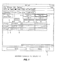
- FIG. 1 is associated with a user interface for the operator's control inputs, and is a simplified line drawing representation of a menu of choices in a SET-UP window that appears on a screen having a screen pointer and an associated mouse and keyboard (neither of which are shown).
- Figure 2 is a line drawing representation of a menu of choices in a RESULTS window, is also mouse driven, and pertains to the display of composite eye diagrams, where the rule for combining component eye diagrams has been selected or specified in yet some other window (not shown).
- window or menu at a higher level of abstraction (and which we have not shown, either) that indicates the SET-UP and RESULTS windows of Figures 1 and 2 as choices (i.e., that's how the SET-UP and RESULTS windows are entered).
- FIG. 1 illustrates a SET-UP window 1 including a Format tab 2 that has been selected to be the "front" tab (in accordance with well known Graphical User Interface [GUI] techniques).
- the Format tab 2 allows the definition of groups. This consists of specifying group names (5, 6 and 7, and which in this example are Groupl, Group2 and Group3, respectively), and the association of channels with those named groups.
- a legend "Pod Cl” appears in a box 3, beneath which are certain indicia, including a row of asterisks in box 9.
- Pod Cl of box 3 means the #1 probe pod installed in the C location.
- the row of asterisks in box 9 corresponds to a natural ordering of the DUT input signals associated with that probe pod, and indicates which ones have been assigned.
- the legend in box 8 indicates the channel assignment names that are associated with the row of asterisks.
- Group1 is sixteen bits from Pod Cl and that the names of the associated channels are C1[15], C1[14], ... C1[0].
- the least significant eight of DUT input signals for Group1 are also assigned to Group2 as C1[7:0].
- Group 3 is C2[7:0].
- There is a small data structure inside the EDA that records all such assignments of channels to groups. We shall be interested in Group 1, and now that we have seen how it was defined, we turn to Figure 2 to see how it is used.
- Figure 2 illustrates a RESULTS window 10 within which is displayed a composite eye diagram 11 for Group1. It is for Group1 because that is the choice that has been selected in box 12.
- the eye diagram 11 is of a particular type of composite (Normalized Signal Density, Average Signal Density, Channel Density) selected in accordance with a menu of such choices found in some convenient location, say, as part of the Measurements tab 15.
- that menu (which is a conventional drop down or other standard GUI type menu) could be a part of the Display tab 14, which in the figure is currently the tab in front.
- Also part of the Display tab 14 is a drop down menu for Display Mode whose current selection is designated by the legend "Gray Scale" in box 13.
- This structure saves the raw measurement data from scanning.
- Information for display is derived from this structure by interpolation. Description of data types u32 unsigned 32 bit integer (0 .. 4 294 967 295) i32 signed 32 bit integer (-2 147 483 648 .. 2 147 483 647) "allocated" memory assigned from a common memory pool by calling an allocation function
- the structure holds two 2-D arrays.
- the two arrays are the same size. Each is kRows by jCols. Array indices start at zero, following the C language convention:
- the cell [I, j] holds information acquired at (tMin + (j * tRes), vMin + (I * vRes)).
- Each cell in pNumClocks gives the number of clock cycles observed at that combination of (T, V) when the measurement was taken. A value of zero means no measurement was taken. If all cells in pNumClocks are zero, then no measurement has been made on this channel.
- Each cell in pNumCounts gives the number of clock cycles where signal activity was observed at that combination of (T, V) when the measurement was taken. This value is less than or equal to the value in the corresponding cell in pNumClocks.
- a CompositeScan structure holds the result of combining ChannelScan measurements from one or more unique channels.
- One useful utility structure is a bit set. BitSet holds the identity of the channel(s) making up the composite and the identity of the channel(s) contributing signal activity at each point in the composite.
- a BitSet structure holds a number (nBits) of one-bit flags. Each flag is either true (1) or false (0). For example, consider a BitSet that represents the channels of an instrument that have been measured. The nBits member is the number of channels in the instrument. The elements in pBits are all zero except for those which have been measured. More specifically, if the instrument has 17 channels and channels 1, 5, and 10 have been measured, then:
- the first two members, channels and channelsWithData, describe the origin of the data for the composite.
- the former gives the set of channels which were given for building the composite.
- the latter gives the set of channels that actually had data that needed to be combined into the composite.
- the nChannelsWithData member is simply for convenience. It equals the number of bits true in channelsWithData. This is the maximum number of channels that may contribute activity at any given point in the composite scan.
- the composite holds the result of merging the data from the channels in channelsWithData.
- the merge must take into account the (possibly) different values for tRes, vRes, tMin, and vMin in each ofthe source measurements. If these are the same for all, then the same values are used in the composite. If not, the smallest values of each are used. Then, the composite's kRows and j Cols are calculated such that the composite covers the largest time and voltage scan positions recorded in the source measurements.
- the composite Since the composite has a resolution in both time and volts at least as high as that of any source measurement, there is either none or one element in each source measurement that corresponds to each element in the composite.
- the actual set of contributing channels at each point is held in the array pContributors, which is a 2-D array of type BitSet.
- the array itself has the same number of rows and columns as the numCounts and numClocks arrays inside composite. Thus, there is a one-to-one correspondence between elements of pContributors, ChannelScan::numCounts, and ChannelScan: :numClocks.
- each BitSet in pContributors has only nChannelsWithData bits defined.
- Bit 0 corresponds to the lowest bit in the original set (bit 1 in this case), bit 1 to bit 5, and bit 2 to bit 10:
- Contributor bit number (bit number in pContributors) 16 0 - 15 0 - 14 0 - 13 0 - 12 0 - 11 0 - 10 1 2 9 0 - 8 0 - 7 0 - 6 0 - 5 1 1 4 0 - 3 0 - 2 0 - 1 1 0 0 0 0 - -
- the i'th bit is set if the i'th channel indicated in channelsWithData (starting from position 0) had a nonzero count at the corresponding position in its own pNumCounts array.
- CompositeScan is built from information in one or more existing ChannelScan structures. The goal is to create a new ChannelScan with the sum of the information in the source structures. There are these four steps:
- Step 1 Considering the entire collection of ChannelScan structures to be built into the CompositeScan:
- nChannelsWithData is zero, then no measured points exist in this collection. Create an empty composite and quit.
- Step 2 Considering only the collection of ChannelScan structures to be built into the CompositeScan that have one or more measured points:
- ceil(x) is the ceiling function, which returns the smallest integer greater than or equal to x.
- Step 3 Build the pNumCounts and pNumClockS arrays
Landscapes
- Physics & Mathematics (AREA)
- Engineering & Computer Science (AREA)
- General Physics & Mathematics (AREA)
- General Engineering & Computer Science (AREA)
- Nonlinear Science (AREA)
- Human Computer Interaction (AREA)
- Dc Digital Transmission (AREA)
- User Interface Of Digital Computer (AREA)
- Controls And Circuits For Display Device (AREA)
Applications Claiming Priority (2)
| Application Number | Priority Date | Filing Date | Title |
|---|---|---|---|
| US61918 | 2002-01-31 | ||
| US10/061,918 US6810346B2 (en) | 2002-01-31 | 2002-01-31 | Composite eye diagrams |
Publications (3)
| Publication Number | Publication Date |
|---|---|
| EP1340990A2 true EP1340990A2 (de) | 2003-09-03 |
| EP1340990A3 EP1340990A3 (de) | 2004-04-07 |
| EP1340990B1 EP1340990B1 (de) | 2006-09-27 |
Family
ID=27658520
Family Applications (1)
| Application Number | Title | Priority Date | Filing Date |
|---|---|---|---|
| EP03250186A Expired - Lifetime EP1340990B1 (de) | 2002-01-31 | 2003-01-13 | Verfahren zur Kreation eines zusammengesetzten Augendiagramms |
Country Status (4)
| Country | Link |
|---|---|
| US (1) | US6810346B2 (de) |
| EP (1) | EP1340990B1 (de) |
| CA (1) | CA2393717A1 (de) |
| DE (1) | DE60308572T2 (de) |
Cited By (2)
| Publication number | Priority date | Publication date | Assignee | Title |
|---|---|---|---|---|
| EP1528703A3 (de) * | 2003-10-31 | 2008-02-06 | Agilent Technologies, Inc. | Messwerkzeuge mit erzwungene Ausrichtung für zusammengesetzte Augendiagramme |
| EP3930222A1 (de) * | 2020-06-22 | 2021-12-29 | Juniper Networks, Inc. | Loopback-augenabtastungen für optischen sendeempfänger |
Families Citing this family (13)
| Publication number | Priority date | Publication date | Assignee | Title |
|---|---|---|---|---|
| WO2002097373A2 (en) * | 2001-05-31 | 2002-12-05 | Lecroy Corporation | Surface mapping and 3-d parametric analysis |
| US7154944B2 (en) * | 2002-10-31 | 2006-12-26 | Agilent Technologies, Inc. | Mask compliance testing using bit error ratio measurements |
| US6804633B2 (en) * | 2003-01-31 | 2004-10-12 | Agilent Technologies, Inc. | Fast eye diagram analyzer uses nearest neighbor transverse to quickly discover basic eye diagrams |
| US7284141B2 (en) * | 2004-02-05 | 2007-10-16 | Anritsu Company | Method of and apparatus for measuring jitter and generating an eye diagram of a high speed data signal |
| US7362836B2 (en) * | 2005-04-27 | 2008-04-22 | Agilent Technologies, Inc. | Method for selecting optimum sampling parameters for a plurality of data receivers having at least one sampling parameter in common |
| US7483477B2 (en) * | 2005-04-27 | 2009-01-27 | Agilent Technologies, Inc. | User interface for selection of sampling parameters in a logic analyzer whose data receivers are in groups each having a separate threshold that is common to the channels within each group |
| JP4955303B2 (ja) * | 2006-03-23 | 2012-06-20 | テクトロニクス・インコーポレイテッド | デジタル信号分析プログラム及び波形表示装置 |
| US9391794B2 (en) * | 2007-05-01 | 2016-07-12 | Mentor Graphics Corporation | Generating worst case test sequences for non-linearly driven channels |
| US7698669B1 (en) * | 2007-05-11 | 2010-04-13 | Altera Corporation | Method and system to evaluate operational characteristics of an electronic circuit |
| US8502821B2 (en) * | 2008-02-04 | 2013-08-06 | C Speed, Llc | System for three-dimensional rendering of electrical test and measurement signals |
| US20140276161A1 (en) * | 2013-03-15 | 2014-09-18 | GestlnTime, Inc. | Method and apparatus for displaying periodic signals generated by a medical device |
| US10216688B2 (en) * | 2016-05-27 | 2019-02-26 | Avago Technologies International Sales Pte. Limited | Systems and methods for accurate transfer margin communication |
| US20230130046A1 (en) * | 2021-10-27 | 2023-04-27 | Canon U.S.A., Inc. | Devices, systems, and methods for displaying stenosis measurements and calculations |
Family Cites Families (8)
| Publication number | Priority date | Publication date | Assignee | Title |
|---|---|---|---|---|
| US4381546A (en) * | 1979-03-02 | 1983-04-26 | Paradyne Corporation | System for the quantitative measurement of impairments in the communication channel of a quadrature amplitude modulation data communication system |
| EP0448322A3 (en) * | 1990-03-23 | 1992-11-25 | Tektronix, Inc. | Automatic extraction of pulseparametrics from multi-valued functions |
| US6151010A (en) | 1996-05-24 | 2000-11-21 | Lecroy, S.A. | Digital oscilloscope display and method therefor |
| US5959607A (en) | 1996-10-17 | 1999-09-28 | Hewlett-Packard Company | Trace coloring system and method for a signal measurement device having a color display |
| US6385252B1 (en) * | 1999-05-28 | 2002-05-07 | Lucent Technologies Inc. | High density multiple digital signal connection interface with reduced cross talk |
| US6728311B1 (en) * | 2000-04-04 | 2004-04-27 | Thomas Eugene Waschura | Apparatus and method for creating eye diagram |
| WO2001082506A1 (en) * | 2000-04-26 | 2001-11-01 | Optovation Corporation | Ac performance monitor with no clock recovery |
| DE60103361T2 (de) | 2001-03-16 | 2005-06-09 | Agilent Technologies Inc., A Delaware Corp., Palo Alto | Bitfehlerratenmessung |
-
2002
- 2002-01-31 US US10/061,918 patent/US6810346B2/en not_active Expired - Fee Related
- 2002-07-17 CA CA002393717A patent/CA2393717A1/en not_active Abandoned
-
2003
- 2003-01-13 EP EP03250186A patent/EP1340990B1/de not_active Expired - Lifetime
- 2003-01-13 DE DE60308572T patent/DE60308572T2/de not_active Expired - Fee Related
Cited By (2)
| Publication number | Priority date | Publication date | Assignee | Title |
|---|---|---|---|---|
| EP1528703A3 (de) * | 2003-10-31 | 2008-02-06 | Agilent Technologies, Inc. | Messwerkzeuge mit erzwungene Ausrichtung für zusammengesetzte Augendiagramme |
| EP3930222A1 (de) * | 2020-06-22 | 2021-12-29 | Juniper Networks, Inc. | Loopback-augenabtastungen für optischen sendeempfänger |
Also Published As
| Publication number | Publication date |
|---|---|
| US6810346B2 (en) | 2004-10-26 |
| US20030158687A1 (en) | 2003-08-21 |
| EP1340990A3 (de) | 2004-04-07 |
| DE60308572T2 (de) | 2007-06-28 |
| DE60308572D1 (de) | 2006-11-09 |
| EP1340990B1 (de) | 2006-09-27 |
| CA2393717A1 (en) | 2003-07-31 |
Similar Documents
| Publication | Publication Date | Title |
|---|---|---|
| EP1340990B1 (de) | Verfahren zur Kreation eines zusammengesetzten Augendiagramms | |
| CA1281775C (en) | Failure information processing in automatic memory tester | |
| US6871152B2 (en) | Method and apparatus for performing eye diagram measurements | |
| US6760676B2 (en) | On-screen tools for eye diagram measurements | |
| EP1560034B1 (de) | Verfahren und Vorrichtung zur Messung und Anzeige von Augenmustermessungen | |
| EP1094320B1 (de) | Test- und Messinstrument mit mehrkanaliger Telekommunikationsmaskentestfähigkeit | |
| JPH0354356B2 (de) | ||
| US6804633B2 (en) | Fast eye diagram analyzer uses nearest neighbor transverse to quickly discover basic eye diagrams | |
| US5731984A (en) | Vector-based waveform acquisition and display | |
| KR100356725B1 (ko) | 반도체 시험 장치 | |
| EP1348973B1 (de) | Identifizierung von Testkanälen und damit zusammenhängenden Signal-Informationen innerhalb eines Datenaugen-Ausschnitts | |
| EP0123381A1 (de) | Gerät zur Wiedergabe logischer Daten | |
| US7386406B2 (en) | Forced-alignment measurement tools for composite eye diagrams | |
| EP1359699A2 (de) | Augenmusteranalysator | |
| EP0290276A2 (de) | Anzeige für digitale Signalformen | |
| Rush et al. | Two ways to catch a wave (oscilloscopes) | |
| US20070088529A1 (en) | Analog display of signal swing and logic analyzer thresholds | |
| JPH07274217A (ja) | ビデオ信号検査方法および装置 | |
| SEQUENCING | Eight-Channel Oscilloscope With Digital Triggering | |
| JPH0772126A (ja) | 測定波形表示装置 |
Legal Events
| Date | Code | Title | Description |
|---|---|---|---|
| PUAI | Public reference made under article 153(3) epc to a published international application that has entered the european phase |
Free format text: ORIGINAL CODE: 0009012 |
|
| AK | Designated contracting states |
Kind code of ref document: A2 Designated state(s): AT BE BG CH CY CZ DE DK EE ES FI FR GB GR HU IE IT LI LU MC NL PT SE SI SK TR |
|
| AX | Request for extension of the european patent |
Extension state: AL LT LV MK RO |
|
| PUAL | Search report despatched |
Free format text: ORIGINAL CODE: 0009013 |
|
| AK | Designated contracting states |
Kind code of ref document: A3 Designated state(s): AT BE BG CH CY CZ DE DK EE ES FI FR GB GR HU IE IT LI LU MC NL PT SE SI SK TR |
|
| AX | Request for extension of the european patent |
Extension state: AL LT LV MK RO |
|
| RIC1 | Information provided on ipc code assigned before grant |
Ipc: 7G 01R 31/319 A Ipc: 7G 01R 31/28 B |
|
| 17P | Request for examination filed |
Effective date: 20040916 |
|
| AKX | Designation fees paid |
Designated state(s): DE FI GB SE |
|
| 17Q | First examination report despatched |
Effective date: 20050217 |
|
| GRAP | Despatch of communication of intention to grant a patent |
Free format text: ORIGINAL CODE: EPIDOSNIGR1 |
|
| RIN1 | Information on inventor provided before grant (corrected) |
Inventor name: HAEFFELE, JEFFREY JOHN Inventor name: NYGAARD, RICHARD A. JR. |
|
| GRAS | Grant fee paid |
Free format text: ORIGINAL CODE: EPIDOSNIGR3 |
|
| GRAA | (expected) grant |
Free format text: ORIGINAL CODE: 0009210 |
|
| AK | Designated contracting states |
Kind code of ref document: B1 Designated state(s): DE FI GB SE |
|
| REG | Reference to a national code |
Ref country code: GB Ref legal event code: FG4D |
|
| REF | Corresponds to: |
Ref document number: 60308572 Country of ref document: DE Date of ref document: 20061109 Kind code of ref document: P |
|
| PG25 | Lapsed in a contracting state [announced via postgrant information from national office to epo] |
Ref country code: FI Free format text: LAPSE BECAUSE OF NON-PAYMENT OF DUE FEES Effective date: 20070113 |
|
| PG25 | Lapsed in a contracting state [announced via postgrant information from national office to epo] |
Ref country code: SE Free format text: LAPSE BECAUSE OF NON-PAYMENT OF DUE FEES Effective date: 20070114 |
|
| REG | Reference to a national code |
Ref country code: SE Ref legal event code: TRGR |
|
| RAP2 | Party data changed (patent owner data changed or rights of a patent transferred) |
Owner name: AGILENT TECHNOLOGIES, INC. |
|
| PLBE | No opposition filed within time limit |
Free format text: ORIGINAL CODE: 0009261 |
|
| STAA | Information on the status of an ep patent application or granted ep patent |
Free format text: STATUS: NO OPPOSITION FILED WITHIN TIME LIMIT |
|
| 26N | No opposition filed |
Effective date: 20070628 |
|
| EUG | Se: european patent has lapsed | ||
| GBPC | Gb: european patent ceased through non-payment of renewal fee |
Effective date: 20070113 |
|
| PG25 | Lapsed in a contracting state [announced via postgrant information from national office to epo] |
Ref country code: GB Free format text: LAPSE BECAUSE OF NON-PAYMENT OF DUE FEES Effective date: 20070113 |
|
| PGFP | Annual fee paid to national office [announced via postgrant information from national office to epo] |
Ref country code: DE Payment date: 20090108 Year of fee payment: 7 |
|
| PG25 | Lapsed in a contracting state [announced via postgrant information from national office to epo] |
Ref country code: DE Free format text: LAPSE BECAUSE OF NON-PAYMENT OF DUE FEES Effective date: 20100803 |