EP1339111B1 - Contact structure, phase change memory cell, and manufacturing method thereof with elimination of double contacts - Google Patents
Contact structure, phase change memory cell, and manufacturing method thereof with elimination of double contacts Download PDFInfo
- Publication number
- EP1339111B1 EP1339111B1 EP02425089A EP02425089A EP1339111B1 EP 1339111 B1 EP1339111 B1 EP 1339111B1 EP 02425089 A EP02425089 A EP 02425089A EP 02425089 A EP02425089 A EP 02425089A EP 1339111 B1 EP1339111 B1 EP 1339111B1
- Authority
- EP
- European Patent Office
- Prior art keywords
- layer
- forming
- thin portion
- region
- resistive element
- Prior art date
- Legal status (The legal status is an assumption and is not a legal conclusion. Google has not performed a legal analysis and makes no representation as to the accuracy of the status listed.)
- Expired - Lifetime
Links
Images


Classifications
-
- G—PHYSICS
- G11—INFORMATION STORAGE
- G11C—STATIC STORES
- G11C11/00—Digital stores characterised by the use of particular electric or magnetic storage elements; Storage elements therefor
- G11C11/56—Digital stores characterised by the use of particular electric or magnetic storage elements; Storage elements therefor using storage elements with more than two stable states represented by steps, e.g. of voltage, current, phase, frequency
- G11C11/5678—Digital stores characterised by the use of particular electric or magnetic storage elements; Storage elements therefor using storage elements with more than two stable states represented by steps, e.g. of voltage, current, phase, frequency using amorphous/crystalline phase transition storage elements
-
- G—PHYSICS
- G11—INFORMATION STORAGE
- G11C—STATIC STORES
- G11C11/00—Digital stores characterised by the use of particular electric or magnetic storage elements; Storage elements therefor
- G11C11/56—Digital stores characterised by the use of particular electric or magnetic storage elements; Storage elements therefor using storage elements with more than two stable states represented by steps, e.g. of voltage, current, phase, frequency
-
- H—ELECTRICITY
- H10—SEMICONDUCTOR DEVICES; ELECTRIC SOLID-STATE DEVICES NOT OTHERWISE PROVIDED FOR
- H10B—ELECTRONIC MEMORY DEVICES
- H10B63/00—Resistance change memory devices, e.g. resistive RAM [ReRAM] devices
- H10B63/30—Resistance change memory devices, e.g. resistive RAM [ReRAM] devices comprising selection components having three or more electrodes, e.g. transistors
- H10B63/32—Resistance change memory devices, e.g. resistive RAM [ReRAM] devices comprising selection components having three or more electrodes, e.g. transistors of the bipolar type
-
- H—ELECTRICITY
- H10—SEMICONDUCTOR DEVICES; ELECTRIC SOLID-STATE DEVICES NOT OTHERWISE PROVIDED FOR
- H10N—ELECTRIC SOLID-STATE DEVICES NOT OTHERWISE PROVIDED FOR
- H10N70/00—Solid-state devices without a potential-jump barrier or surface barrier, and specially adapted for rectifying, amplifying, oscillating or switching
- H10N70/011—Manufacture or treatment of multistable switching devices
- H10N70/061—Patterning of the switching material
- H10N70/068—Patterning of the switching material by processes specially adapted for achieving sub-lithographic dimensions, e.g. using spacers
-
- H—ELECTRICITY
- H10—SEMICONDUCTOR DEVICES; ELECTRIC SOLID-STATE DEVICES NOT OTHERWISE PROVIDED FOR
- H10N—ELECTRIC SOLID-STATE DEVICES NOT OTHERWISE PROVIDED FOR
- H10N70/00—Solid-state devices without a potential-jump barrier or surface barrier, and specially adapted for rectifying, amplifying, oscillating or switching
- H10N70/20—Multistable switching devices, e.g. memristors
- H10N70/231—Multistable switching devices, e.g. memristors based on solid-state phase change, e.g. between amorphous and crystalline phases, Ovshinsky effect
-
- H—ELECTRICITY
- H10—SEMICONDUCTOR DEVICES; ELECTRIC SOLID-STATE DEVICES NOT OTHERWISE PROVIDED FOR
- H10N—ELECTRIC SOLID-STATE DEVICES NOT OTHERWISE PROVIDED FOR
- H10N70/00—Solid-state devices without a potential-jump barrier or surface barrier, and specially adapted for rectifying, amplifying, oscillating or switching
- H10N70/801—Constructional details of multistable switching devices
- H10N70/821—Device geometry
- H10N70/826—Device geometry adapted for essentially vertical current flow, e.g. sandwich or pillar type devices
-
- H—ELECTRICITY
- H10—SEMICONDUCTOR DEVICES; ELECTRIC SOLID-STATE DEVICES NOT OTHERWISE PROVIDED FOR
- H10N—ELECTRIC SOLID-STATE DEVICES NOT OTHERWISE PROVIDED FOR
- H10N70/00—Solid-state devices without a potential-jump barrier or surface barrier, and specially adapted for rectifying, amplifying, oscillating or switching
- H10N70/801—Constructional details of multistable switching devices
- H10N70/841—Electrodes
- H10N70/8413—Electrodes adapted for resistive heating
-
- H—ELECTRICITY
- H10—SEMICONDUCTOR DEVICES; ELECTRIC SOLID-STATE DEVICES NOT OTHERWISE PROVIDED FOR
- H10N—ELECTRIC SOLID-STATE DEVICES NOT OTHERWISE PROVIDED FOR
- H10N70/00—Solid-state devices without a potential-jump barrier or surface barrier, and specially adapted for rectifying, amplifying, oscillating or switching
- H10N70/801—Constructional details of multistable switching devices
- H10N70/881—Switching materials
- H10N70/882—Compounds of sulfur, selenium or tellurium, e.g. chalcogenides
- H10N70/8828—Tellurides, e.g. GeSbTe
-
- G—PHYSICS
- G11—INFORMATION STORAGE
- G11C—STATIC STORES
- G11C13/00—Digital stores characterised by the use of storage elements not covered by groups G11C11/00, G11C23/00, or G11C25/00
- G11C13/0002—Digital stores characterised by the use of storage elements not covered by groups G11C11/00, G11C23/00, or G11C25/00 using resistive RAM [RRAM] elements
- G11C13/0004—Digital stores characterised by the use of storage elements not covered by groups G11C11/00, G11C23/00, or G11C25/00 using resistive RAM [RRAM] elements comprising amorphous/crystalline phase transition cells
Description
- The present invention relates to a contact structure, a phase change memory cell, and a manufacturing process thereof.
As is known, phase change memory (PCM) elements exploit the characteristics of materials which have the property of changing between two phases having distinct electrical characteristics. For example, these materials may change from an amorphous phase, which is disorderly, to a crystalline or polycrystalline phase, which is orderly, and the two phases are associated to considerably different resistivity. - At present, alloys of group VI of the periodic table, such as Te or Se, referred to as chalcogenides or chalcogenic materials, can advantageously be used in phase change cells. The chalcogenide that currently offers the most promise is formed by a Ge, Sb and Te alloy (Ge2Sb2Te5), which is currently widely used for storing information in overwritable disks.
- In chalcogenides, the resistivity varies by two or more magnitude orders when the material passes from the amorphous phase (more resistive) to the polycrystalline phase (more conductive) and vice versa. The characteristics of chalcogenides in the two phases are shown in Figure 1. As may be noted, at a given read voltage, here designated by Vr, there is a resistance variation of more than 10.
- Phase change may be obtained by locally increasing the temperature, as shown in Figure 2. Below 150°C both phases are stable. Above 200°C (temperature of start of nucleation, designated by Tx) , fast nucleation of the crystallites takes place, and, if the material is kept at the crystallization temperature for a sufficient length of time (time t2), it changes its phase and becomes crystalline. To bring the chalcogenide back into the amorphous state, it is necessary to raise the temperature above the melting temperature Tm (approximately 600°C) and then to cool the chalcogenide off rapidly (time t1).
- From the electrical standpoint, it is possible to reach both critical temperatures, namely the crystallization temperature and the melting point, by causing a current to flow through a resistive element which heats the chalcogenic material by the Joule effect.
- The basic structure of a
PCM element 1 which operates according to the principles described above is shown in Figure 3 and comprises a resistive element 2 (heater) and aprogrammable element 3. Theprogrammable element 3 is made of a chalcogenide and is normally in the polycrystalline state in order to enable a good flow of current. One part of theprogrammable element 3 is in direct contact with theresistive element 2 and forms the area affected by phase change, hereinafter referred to as thephase change portion 4. - If an electric current having an appropriate value is caused to pass through the
resistive element 2, it is possible to heat thephase change portion 4 selectively up to the crystallization temperature or to the melting temperature and to cause phase change. In particular, if a current I flows through aresistive element 2 having resistance R, the heat generated is equal to I2R. - The use of the PCM element of Figure 3 for forming memory cells has already been proposed. In order to prevent noise caused by adjacent memory cells, the PCM element is generally associated to a selection element, such a MOS transistor, a bipolar transistor, or a diode.
- All the known approaches are, however, disadvantageous due to the difficulty in finding solutions that meet present requirements as regards capacity for withstanding the operating currents and voltages, as well as functionality and compatibility with present CMOS technologies.
- In particular, considerations of a technological and electrical nature impose the creation of a contact area of small dimensions, preferably 20 nm x 20 nm, between the chalcogenic region and a resistive element. However, these dimensions are much smaller than those that can be obtained with current optical (UV) lithographic techniques, which scarcely reach 100 linear nm.
- To solve the above problem, patent application 01128461.9 (
publication number 1 318 552 A1), filed on 5.12.2001, and entitled "Small area contact region, high efficiency phase change memory cell, and manufacturing method thereof", teaches forming the contact area as an intersection of two thin portions extending transversely with respect to one another and each of a sublithographic size. In order to form the thin portions, deposition of layers is adopted instead of a lithographic process, given that deposition makes it possible to obtain very thin layers, i.e., having a thickness much smaller than the current minimum size that can be achieved using lithographic techniques. - For a better understanding of the problem of the present invention, the manufacturing process object of the above mentioned patent application No. 01128461.9 will now be described.
- With reference to Figure 4, initially a
wafer 10 comprising a P-type substrate 11 is subjected to standard front end steps. In particular, inside thesubstrate 11insulation regions 12 are formed and delimitactive areas 16; then, in succession, N-type base regions 13, N+-typebase contact regions 14, and P+-type emitter regions 15 are implanted. Thebase regions 13,base contact regions 14, andemitter regions 15 form diodes that form selection elements for the memory cells. - Next, a first
dielectric layer 18 is deposited and planarized; openings are formed in the firstdielectric layer 18 above thebase contact regions 13 andemitter regions 15, and the openings are filled with tungsten to formbase contacts 19b andemitter contacts 19a. Thebase contacts 19b are thus in direct electrical contact with thebase contact regions 13, and theemitter contacts 19a are in direct electrical contact with theemitter regions 15. Advantageously, the openings in the firstdielectric layer 18 can be covered by a barrier layer, for example a Ti/TiN layer, before being filled with tungsten. In this way, the structure of Figure 4 is obtained. - Figure 5 shows the layout of some masks used for forming the structure of Figure 4 regarding a pair of
memory cells 5 that are adjacent in a perpendicular direction to the sectional plane of Figure 4 (Y direction) . In particular, the figure shows a mask A used for defining theactive areas 16, a mask B used for implanting theemitter regions 15, and a mask C for forming the openings where thebase contacts 19b and theemitter contacts 19a are to be formed. Figure 4 is a cross-section taken along line IV-IV of Figure 5, while Figure 6 shows the same structure sectioned along the section line VI-VI of Figure 5. - Next (Figure 7), a second dielectric layer 20 -for example, an undoped silicon glass (USG) layer- is deposited, and
openings 21 are formed in the seconddielectric layer 20 above theemitter contact 19a. Theopenings 21 have dimensions dictated by the lithographic process and are, for example, circle-shaped. Next, a heating layer, for example of TiSiN, TiAlN or TiSiC, is deposited for a thickness of 10-50 nm, preferably 20 nm. The heating layer, designed to form theresistive element 2 of Figure 3, conformally coats the walls and bottom of theopenings 21 and is subsequently removed outside theopenings 21. The remaining portions of the heating layer thus form a cup-shaped region 22 and are then filled withdielectric material 23. - Next, as shown in the enlarged detail of Figure 8, a
mold layer 27, for instance USG having a thickness of 20 nm, anadhesion layer 28, for instance Ti or Si with a thickness of 5 nm, and afirst delimiting layer 29, for example nitride or another material that enables selective etching with respect to theadhesion layer 28, are deposited in sequence. Thefirst delimiting layer 29 has a thickness of, for instance, 150 nm. Then, using a mask, one part of thefirst delimiting layer 29 is removed by dry etching to form a step which has avertical side 30 that extends vertically on top of thedielectric material 23. The structure shown in Figure 8 is thus obtained. - Next (Figure 9), a
sacrificial layer 31, for example TiN with a thickness of 30 nm, is deposited conformally. In particular, the sacrificial layer forms avertical wall 31a that extends along thevertical side 30 of thefirst delimiting layer 29. - Next (Figure 10), the
sacrificial layer 31 undergoes an etch back that results in removal of the horizontal portions of thesacrificial layer 31 and of part of thevertical wall 31a. By appropriately choosing the thickness of thefirst delimiting layer 29 and the thickness of thesacrificial layer 31, as well as the time and type of etching, it is possible to obtain the desired sublithographic width W1 for the bottom part of the remainingvertical wall 31a. - As shown in Figure 11, a
second delimiting layer 35, of the same material as thefirst delimiting layer 29, for example nitride, with a thickness of 300 nm, is deposited. Next, thedelimiting layers vertical wall 31a are thinned by Chemical Mechanical Polishing (CMP). At the end, the remaining portions of the delimitinglayers sacrificial region 36. - Next (Figure 12), the
sacrificial region 36 is removed. Theadhesion layer 28 is isotropically etched, and themold layer 27 is dry etched to form aslit 37 in themold layer 27, theslit 37 having a width W1 equal to the width of thesacrificial region 36. - Next (Figure 13), the
delimiting layers chalcogenic layer 38, for example of Ge2Sb2Te5 with a thickness of 60 nm, is deposited conformally. Theportion 38a of thechalcogenic layer 38 fills theslit 37 and forms, at the intersection with the cup-shaped region 22, a phase change region similar to thephase change portion 4 of Figure 3. Then, on top of thechalcogenic layer 38 abarrier layer 39, for example of Ti/TiN, and ametal layer 40, for example of AlCu, are deposited. The structure of Figure 13 is thus obtained. - Next (Figure 14), the stack formed by the
metal layer 40,barrier layer 39,chalcogenic layer 38, andadhesion layer 28 is defined using a same mask to form abit line 41. Finally, a thirddielectric layer 42 is deposited, which is opened above thebase contacts 19b. The openings thus formed are filled with tungsten to formtop contacts 43 in order to prolong upwards thebase contacts 19b. Then standard steps are performed for forming the connection lines for connection to thebase contacts 19b and to thebits lines 41, and the final structure of Figure 14 is thus obtained. - In practice, as shown in Figure 15, the intersection between the cup-
shaped region 22 and thethin portion 38a of thechalcogenic layer 38 forms acontact area 45 which is approximately square and has sublithographic dimensions. This is due to the fact that both the cup-shaped region 22 and thethin portion 38a have a width equal to the thickness of a deposited layer. In fact, the width of the cup-shaped region 22 is given by the thickness of the heating layer, and the width of thethin portions 38a is determined by the thickness of thesacrificial layer 31 along thevertical side 30. In greater detail, in the proximity of thecontact area 45, the cup-shapedregion 22 has a sublithographic dimension in a first direction (Y direction), and thethin portion 38a has a sublithographic dimension (width W1 of Figure 10) in a second direction (X direction) which is transverse to the first direction. Hereinafter, the term "sublithographic dimension" means a linear dimension smaller than the limit dimension achievable with current optical (UV) lithographic techniques, and hence smaller than 100 nm, preferably 50-60 nm, down to approximately 20 nm. - In the process described above, forming the
thin portion 38a of thechalcogenic layer 38 entails numerous steps and is somewhat complex. Consequently, it is desirable to avail a simpler alternative process. - In addition, the dimensions of the
contact area 45 depend upon the alignment tolerances between the mask used for forming theopenings 21 and the mask used for removing part of thefirst delimiting layer 29 and for forming the vertical side 30 (Figure 8). In fact, as emerges clearly from a comparison between Figures 16a and 16b which are top plan views of thecontact area 45, in the case of a cup-like region 22 having a circular shape and a diameter of approximately 0.2 µm, an alignment error of even only 0.05 µm between the two masks results in thethin portions 38a no longer crossing the cup-shapedregions 22 perpendicularly, with a consequent considerable increase in the dimensions of the contact area 45 (see Figure 16b) and hence a considerable increase in the flowing current, the value whereof would be uncontrollable. - Furthermore, the
thin portion 38a crosses each cup-shapedregion 22 in two points, thus doubling the total contact area between thethin portions 38a and the cup-shapedregions 22, and consequently also increasing the programming current. In the case of a marked misalignment between the two above masks, just one contact area is even obtained which has dimensions far greater than the requirements. The presence of a double contact gives rise to functional problems, given that in this situation it would be impossible to know which of the twocontact areas 45 first causes switching of the overlyingthin portion 38a (i.e., the phase change portion), nor would it be possible to be certain that both of thethin portions 38a overlying the two contact areas will switch. - The aim of the present invention is to simplify and improve the process described in patent application 01128461.9, with particular regard to the problem of the total contact area between the cup-shaped
region 22 and thethin portion 38a. - According to the present invention there are provided a contact structure, a phase change memory cell, and a manufacture process thereof, as defined in
claims Claims 8 and 21 define a memory array and a process for forming a pair of adjacent memory cells. - For a better understanding of the present invention, a preferred embodiment thereof is now described, purely by way of non-limiting example, with reference to the attached drawings, wherein:
- Figure 1 shows the current versus voltage characteristic of a phase change material;
- Figure 2 shows the temperature versus current plot of a phase change material;
- Figure 3 shows the basic structure of a PCM memory element;
- Figure 4 shows a cross section of a wafer of semiconductor material in a manufacturing step of the cell of Figure 3, according to the aforementioned patent application;
- Figure 5 shows the layout of some masks used for forming the structure of Figure 4;
- Figure 6 is a cross-section taken along line VI-VI of Figure 5;
- Figures 7-14 are cross-section of the structure of the above mentioned patent application, in successive manufacture steps;
- Figure 15 is a top plan view, with parts removed and at an enlarged scale, of a detail of Figure 4;
- Figures 16a and 16b are top plan views, with parts removed, of a detail of Figure 14, in two different manufacture conditions;
- Figure 17 shows the layout of some masks used for forming the structure of Figure 7, according to a first embodiment of the invention;
- Figure 18 is a cross-section of the structure, analogous to Figure 8, in a fabrication step according to the first embodiment;
- Figure 19 shows the layout of some masks used for forming the structure of Figure 18;
- Figures 20 and 21 are cross-sections, similar to Figure 18, in successive manufacture steps according to the invention;
- Figure 22 is a top plan view of the structure of Figure 21;
- Figure 23 is a cross-section, similar to Figure 21, in a subsequent manufacture step;
- Figure 24 shows the layout of same masks used for forming the structure of Figure 23;
- Figure 25 is a cross-section, similar to Figure 14, in a final manufacture step according to the invention;
- Figures 26a and 26b are top plan views of the contact area, in two different manufacture conditions; and
- Figure 27 shows the layout of some masks used after forming the structure of Figure 10, according to a different embodiment of the invention; and
- Figure 28 is a top plan view of the structure obtained with the masks of Figure 27.
- In the following description, parts that are the same as those previously described with reference to Figures 4-14 are designated by the same reference numbers.
- The process according to the present invention comprises initial steps equal to those described in patent application 01128461.9 illustrated above, up to deposition of the second dielectric layer 20 (Figure 7). Next, also here the
openings 21 and the cup-shapedregions 22 are formed. However, as shown in Figure 17, for the definition of theopenings 21, a heater mask D is used which has rectangular windows (the term "rectangular" also comprising the particular case of a square shape). Consequently, theopenings 21 have a substantially rectangular shape. Then the heating layer, for example of TiSiN, TiAlN or TiSiC, with a thickness of 10-50 nm, preferably 20 nm, is deposited. The heating layer coats the walls and bottom of theopenings 21 conformally. Consequently, in top plan view, the cup-like regions 22 here define an ideally rectangular shape, possibly with rounded edges (on account of the lithographic limits), or at the most an ovalized shape, with the longer side, or main direction, parallel to the X direction (Figure 22). Next, the heating layer is removed outside theopenings 21 to form the cup-shapedregions 22, which are then filled with thedielectric material 23. - Then (Figure 18), a
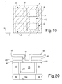
stop layer 48, for example of nitride deposited by PECVD (Plasma Enhanced Chemical Vapor Deposition) with a thickness of 40 nm, amold layer 49, for example of USG deposited by PECVD or SACVD (Sub-Atmospheric Chemical Vapor Deposition) with a thickness of 50-70 nm, and anadhesion layer 50, for example of Ti or Si with a thickness of 20-40 nm, are deposited in sequence. - Next, using a minitrench mask, designated by E in Figure 19, the
adhesion layer 50, themold layer 49 and thestop layer 48 are etched. As shown in Figure 19, the minitrench mask E has a rectangular window that extends between twoadjacent cells 5 in the Y direction (perpendicular to the alignment direction of the base andemitter regions memory cell 5, Figure 7). - Following upon etching, part of the
layers opening 51 having a rectangular shape, corresponding to that of the minitrench mask E. The width of theopening 51 in the X direction is, for example, 160 nm. Theopening 51 uncovers part of thedielectric material 23 of the twoadjacent cells 5 and crosses each cup-shapedregion 22 only once, as can be clearly seen from the superposition of the heater mask D and minitrench mask E in Figure 19. - Next, Figure 20, a
spacer layer 55, for example an oxide layer, is deposited (in particular, TEOS with a thickness of 50 nm). Thespacer layer 55 covers theadhesion layer 50, as well as the walls and bottom of theopening 51. - Then, Figure 21, the
spacer layer 55 is anisotropically etched back until the horizontal portions thereof are removed, according to the well known spacer formation technique. Thespacer layer 55 is then completely removed above theadhesion layer 50 and is partially removed from the bottom of theopening 51 to form aspacer region 55a which extends along the vertical sides of the opening 51 (along the perimeter of a rectangle or of an oval) and delimits aslit 56, the base whereof forms arectangular strip 57 having a sublithographic width W2 (in the X direction) of approximately 60 nm. Figure 22 is a top plan view of the structure thus obtained, and highlights how thestrip 57 uncovers only one portion of the cup-shapedregion 22 of eachcell 5, shown with dashed line in the figure. The uncovered portion of each cup-shapedregion 22 forms acontact area 58, as will be explained hereinafter. - Next, Figure 23, the chalcogenic layer 38 (also in the present case, for instance, of Ge2Sb2Te5 with a thickness of 60 nm), the
barrier layer 39, and themetal layer 40 are deposited in succession, to form a stack oflayers 41. Thechalcogenic layer 38 is in direct contact with theadhesion layer 50, to which it adheres properly, and fills theslit 56 with athin portion 38a. In particular, thethin portion 38a of thechalcogenic layer 38 deposits on thestrip 57, contacting the cup-shapedregions 22 at thecontact areas 58. The inclined wall formed by thespacer region 55a favors filling of theslit 56, so preventing problems linked to a poor aspect ratio of theopening 51. - Next, the stack of
layers 41 is defined using a stack mask F (Figure 24). - The process continues with the steps described previously, which comprise deposition of the
third dielectric layer 42, opening of thethird dielectric layer 42 above thebase contacts 19b, formation of thetop contacts 43, and formation of connection lines for connection to thebase contacts 19b and to the bit lines 41, so as to obtain the final structure shown in Figure 25. - According to a different embodiment, the
thin portion 38a of thechalcogenic layer 38 is formed using the technology described in the aforementioned patent application No. 01128461.9, and the second crossing-over between the cup-shapedregion 22 and thethin portion 38a is avoided by using a special mask referred to as "rapier-selection mask", as described hereinafter. - In detail, the process comprises initial steps that are the same as those described with reference to Figures 4-9, with the sole difference that the cup-shaped
region 22 is preferably formed using the mask of Figure 17 so as to obtain a rectangular shape or at the most an oval shape on account of the lithographic limits. At this point, thevertical wall 31a is present on thestep 30 of thefirst delimitation layer 29, and the rest of thesacrificial layer 31 has already been removed. - Next, using an appropriate mask referred to as "rapier-selection mask" G, illustrated in Figure 27, part of the
vertical wall 31a is removed so that this wall intersects the cup-shapedregion 22 of eachshell 5 in just one point. In detail, the rapier-selection mask G covers a strip which extends parallel to the direction X bestriding twocells 5. The portions of thevertical wall 31a not covered by the rapier-selection mask G are then removed. In this way, as illustrated in the top plan view of Figure 28 regarding twoadjacent cells 5, at the side of thestep 30 there remains just one portion ofvertical wall 31a, the section of which in the X-Z plane coincides with that of Figure 10 described above. As may be noted, the remaining portion ofvertical wall 31a intersects each cup-shapedregion 22 just once, as is highlighted by the hatched area which will subsequently come to form thecontact area 45. - The process goes on with the same steps as those described above with reference to Figures 11-14, and then with deposition of the
second delimitation layer 35; thinning of the delimitation layers 35 and 29, as well as of thevertical wall 31a until the structure of Figure 11 is obtained; removal of thesacrificial portion 36 and etching of the adhesion layers 28 and of the mold layer 27 (Figure 12); deposition of thechalcogenic layer 38 which fills theslit 37 of themold layer 27; deposition of thebarrier layer 39 and of themetal layer 40; shaping of the stack formed by themetal layer 40, thebarrier layer 39, thechalcogenic layer 38 and theadhesion layer 28; deposition of thethird dielectric layer 42; and the final steps described above for obtaining the structure illustrated in Figure 14. - In practice, in both of the embodiments
thin portions 38a are formed having a roughly parallelepiped shape and short length, i.e., smaller than the overall dimensions of twocells 5 in the Y direction. In the first embodiment, thethin portion 38a is delimited by thespacer region 55a; in the second embodiment, thethin portion 38a is delimited directly by themold layer 27. - The advantages of the process and structure described are illustrated hereinafter. First, it is possible to obtain just one
contact area region 22, and thus for eachcell 5; thereby the total contact area is reduced, so solving the problems highlighted above. - The elimination of the second contact can be obtained without requiring additional masking steps in the case where the
thin region 38a is defined according to the first embodiment, using the minitrench technique thanks to the shape of the minitrench mask E. - With the second embodiment (i.e. using the rapier-selection mask G) the process allows instead smaller and more controllable dimensions by adding a special mask.
- The rectangular or ovalized shape of the cup-shaped
region 22 reduces the spread in the dimensions of thecontact area region 22 with respect tothin region 38a in the absence of mask misalignment, and Figure 26b, which shows the relative position in presence of misalignment. - Finally, it is clear that numerous modifications and variations may be made to the process and to the memory cell described and illustrated herein, all falling within the scope of the invention, as defined in the attached claims. For example, the sequence of steps required for forming the
spacer region 55a and of thestrip 57 may vary. In particular, for forming theopening 51 it is possible to etch theadhesion layer 50 and themold layer 49 alone, without removing thestop layer 48. Next, thespacer region 55a is formed in the way described previously, by depositing a spacer layer and etching it anisotropically. Then, thestop layer 48 is removed only where it is not covered by thespacer region 55a, and in this way thestrip 57 is uncovered. Before depositing thespacer layer 55, a nitride layer may be deposited and removed from the horizontal portions during the etch back so as to remain only under thespacer region 55a. This further nitride layer protects theadhesion layer 50 and prevents the latter to be contaminated by thespacer layer 55, of oxide, both upwardly and on the lateral sides. It also acts as an etch stop and avoid an undesired etching of thedielectric layer 20 and thedielectric material 23 during etch back when forming thespacer region 55a. - Furthermore, in the second embodiment, a stop layer may be deposed before the mold layer, analogously to what described for the first embodiment. Finally, when an adhesion layer is not required, the process according to the second embodiment may be simplified so as to form the delimitation layers 29, 35 directly on the insulating
layer 20. In this case, the delimitation layers 29, 35 form themselves a mold layer and when thesacrificial region 31a is removed, theslit 37 is directly obtained.
Claims (25)
- A contact structure in a semiconductor electronic device, comprising:a first conductive region (22) and a second conductive region (38) of a phase change material which extends on top of said first conductive region (22),said first conductive region (22) comprising a closed-shape wall including a first thin portion having a first sublithographic dimension in a first direction (Y);said second conductive region (38) comprising a second thin portion (38a) having a second sublithographic dimension in a second direction (X) transverse to said first dimension, said second thin portion crossing, and being in direct electrical contact with, said first conductive region only at said first thin portion (22) so as to form a single contact area (45, 58) having a sublithographic extension.
- A phase-change memory cell (5) comprising a resistive element (22) and a memory region (38) made of a phase-change material, which extends on top of said resistive element;
said resistive element comprising a wall having a closed shape including a first thin portion (22) having a first sublithographic dimension in a first direction (Y);
said memory region (38) comprising a second thin portion (38a) having a second sublithographic dimension in a second direction (X) transverse to said first dimension, said second thin portion (38a) crossing, and being in direct electrical contact with, said first resistive element only at said first thin portion (22) so as to form a single contact area (45, 58) having a sublithographic extension. - The memory cell according to claim 2, wherein said second thin portion (38a) is surrounded by a mold layer (27, 49) of a second dielectric material, which forms an opening (37; 51) having an approximately rectangular shape.
- The memory cell according to claim 3, wherein said second thin portion (38a) is delimited on the side by, and is in direct contact with said mold layer (27), and said opening (37) has a sublithographic dimension.
- The memory cell according to claim 3, wherein said second thin portion (38a) is surrounded by a spacer region (55a) housed in said opening (51), and said opening is of lithographic dimension.
- The memory cell according to claim 5, wherein said resistive element (22) is formed inside an insulating layer (20), said mold layer (49) extends above said insulating layer, and a stop layer (48) extends between said insulating layer and said mold layer, said spacer region being of silicon dioxide, said mold layer (49) and said insulating layer (20) being of a silicon glass, and said stop layer (48) being of silicon nitride.
- The memory cell according to any one of claims 2 to 6, wherein said closed line (22) is chosen between rectangular and elongated oval.
- A memory array comprising at least two memory cells (5), each of which has a respective resistive element (22) having a closed-shape wall including a first thin portion having a first sublithographic dimension in a first direction (Y), said two memory cells further comprising a common memory region (38) of a phase change material extending above said resistive element (22) and including a second thin portion (38a) having a second sublithographic dimension in a second direction (X) transverse to said first dimension;
wherein said memory cells (5) are adjacent to one another in said first direction (Y);
each resistive element crossing, and being in direct electrical contact with, said second thin region (38a) only in a point of said first thin portion (22) so as to form a respective single contact area (58) having a sublithographic extension. - The memory array according to claim 8, wherein said second thin portion (38a) has an elongated shape and extends substantially along said first direction (Y) between said two memory cells (5).
- A process for manufacturing a contact structure in a semiconductor electronic device, comprising:forming a first conductive region (22) comprising a wall having a closed shape including a first thin portion having a first sublithographic dimension in a first direction (Y); andforming a second conductive region (38) of a phase change material, said second conductive region including a second thin portion (38a) having a second sublithographic dimension extending in a second direction (X) transverse to said first dimension, said second thin portion crossing, and being in direct electrical contact with, said first conductive region (22) only at said first thin portion (22) so as to form a single contact area (45, 58) having a sublithographic extension.
- A process for manufacturing a phase change memory cell, comprising:forming a resistive element (22) comprising a closed-shape wall including a first thin portion having a first sublithographic dimension in a first direction (Y); andforming a memory region (38) of a phase change material, the memory region including a second thin portion (38a) having a second sublithographic dimension extending in a second direction (X) transverse to said first dimension, said second thin portion crossing, and being in direct electrical contact with, said resistive element only at said first thin portion (22) so as to form a single contact area (45, 58) having a sublithographic extension.
- The process according to claim 11, wherein said step of forming a memory region (38) comprises forming a mold structure (27; 49, 55a) on top of said resistive element (22), said mold structure having a slit (37, 56) crossing said first thin portion (22) only in a point, said slit having said second sublithographic dimension; depositing a phase change layer (38) at least inside said slit; and forming said second thin portion (38a).
- The process according to claim 12, wherein said step of forming a mold structure (49, 55a) comprises depositing a mold layer (49); forming a first lithographic opening (51) in said mold layer; and forming spacer portions (55a) in said first lithographic opening, said spacer portions delimiting said slit (56).
- The process according to claim 13, wherein said step of forming spacer portions (55a) comprises, after said step of forming a first lithographic opening (51), depositing a spacer layer (55) and anisotropically etching said spacer layer.
- The process according to claim 13 or 14, wherein said spacer portions (55a) are of a first dielectric material and have surfaces inclined in a third direction transverse to said first and second directions, and said mold layer (49) is of a second dielectric material, wherein, prior to said step of forming a mold layer (49), a stop layer (48) of a third dielectric material is formed on top of said resistive element (22).
- The process according to claim 12, wherein said resistive element (22) is formed in an insulating layer (20) and said step of forming a mold structure (27) comprises depositing a first delimitation layer (29) on top of said insulating layer, said first delimitation layer (29) forming a step having a vertical wall (30) extending transversely to said first thin portion (22); forming a sacrificial portion (31a) along said vertical wall; removing part of said sacrificial portion (31a) to form a sacrificial region (31a) that crosses said resistive element (22) in just one point; forming a second delimitation area (35) extending above said insulating layer (20) and at the sides of said sacrificial region (31a), as well as of said first delimitation layer (29); and removing said sacrificial region to form a delimitation opening.
- The process according to claim 16, wherein, before forming a first delimitation layer (29), the step is carried out of depositing a mold layer (27) on top of said insulating layer (20); and in which, after said step of removing said sacrificial region (31a), the steps are carried out of forming said slit (37) in said mold layer (27) underneath said delimitation opening, and removing said first delimitation layer (29) and said second delimitation layer (35).
- The process according to any one of claims 12 to 17, wherein said step of forming a resistive element (22) comprises forming a second lithographic opening (21) in an insulating layer (20), depositing a conductive layer (22) on a side wall of said second lithographic opening and filling (23) said second lithographic opening.
- The process according to any one of claims 12 to 18, wherein said resistive element (22) is cup-shaped and comprises a vertical side which extends, in top plan view, along a closed line chosen between rectangular and elongated oval.
- The process according to any one of claims 12 to 19, wherein said step of forming a mold structure (27; 49, 55a) comprises depositing a mold layer (27; 49), depositing an adhesion layer (50), and opening said mold layer and said adhesion layer.
- A process for forming a pair of adjacent memory cells (5) in a first direction (Y), comprising the steps of:forming a pair of resistive elements (22), each having a closed-shape wall and a first thin portion of a first sublithographic dimension in said first direction (Y),forming a common memory region (38) of a phase change material including a second thin portion (38a) in direct electrical contact with said first thin portions and having a second sublithographic dimension in a second direction (X) transverse to said first dimension;each resistive element forming, with said second thin region, a respective single contact area (45; 58) having a sublithographic extension.
- The process according to claim 21, wherein said step of forming a common memory region (38) comprises forming a mold structure (27; 49, 55a) having a slit (37; 56) extending between said pair of resistive elements (22) and crossing each said first thin portion (22) of said resistive elements just in one point; said slit having said second sublithographic dimension; and depositing a phase change layer (38) at least inside said slit, and forming said second thin portion (38a).
- The process according to claim 22, wherein said step of forming a mold structure comprises forming a mold layer (49) on top of said resistive element (22); forming a lithographic opening (51) in said mold layer; and forming spacer portions (55a) in said lithographic opening, said spacer portions delimiting said slit (56).
- The process according to claim 23, wherein said resistive element is formed in an insulating layer (20) and said step of forming a mold structure (27) comprises depositing a mold layer (27) on top of said insulating layer; depositing a first delimitation layer (29) on top of said mold layer, said first delimitation layer (29) forming a step having a vertical wall (30) extending transversely with respect to said first thin portion (22) of said pair of cells; forming a sacrificial portion (31a) along said vertical wall; removing part of said sacrificial portion to form a sacrificial region (31a) which extends between said pair of cells (5) and crosses each said resistive element (22) only in a respective point; forming a second delimitation layer (35) on top of said insulating layer (20) and laterally to said sacrificial region and said first delimitation layer; removing said sacrificial region (31a) to form a delimitation opening; forming said slit (37) in said mold layer (27), underneath said delimitation opening; and removing said first and second delimitation layers.
- The process according to claim 24, wherein said step of removing part of said sacrificial portion (31a) comprises depositing a mask (G) covering a region bestriding said pair of cells (5) and including said first thin portion (22) of said pair of cells.
Priority Applications (4)
| Application Number | Priority Date | Filing Date | Title |
|---|---|---|---|
| EP02425089A EP1339111B1 (en) | 2002-02-20 | 2002-02-20 | Contact structure, phase change memory cell, and manufacturing method thereof with elimination of double contacts |
| DE60220015T DE60220015T2 (en) | 2002-02-20 | 2002-02-20 | Contact structure, phase change memory cell and their production process with elimination of double contacts |
| US10/372,639 US6930913B2 (en) | 2002-02-20 | 2003-02-20 | Contact structure, phase change memory cell, and manufacturing method thereof with elimination of double contacts |
| US11/156,989 US7402455B2 (en) | 2002-02-20 | 2005-06-20 | Manufacturing method of a contact structure and phase change memory cell with elimination of double contacts |
Applications Claiming Priority (1)
| Application Number | Priority Date | Filing Date | Title |
|---|---|---|---|
| EP02425089A EP1339111B1 (en) | 2002-02-20 | 2002-02-20 | Contact structure, phase change memory cell, and manufacturing method thereof with elimination of double contacts |
Publications (3)
| Publication Number | Publication Date |
|---|---|
| EP1339111A1 EP1339111A1 (en) | 2003-08-27 |
| EP1339111A9 EP1339111A9 (en) | 2004-01-28 |
| EP1339111B1 true EP1339111B1 (en) | 2007-05-09 |
Family
ID=27635930
Family Applications (1)
| Application Number | Title | Priority Date | Filing Date |
|---|---|---|---|
| EP02425089A Expired - Lifetime EP1339111B1 (en) | 2002-02-20 | 2002-02-20 | Contact structure, phase change memory cell, and manufacturing method thereof with elimination of double contacts |
Country Status (2)
| Country | Link |
|---|---|
| EP (1) | EP1339111B1 (en) |
| DE (1) | DE60220015T2 (en) |
Families Citing this family (10)
| Publication number | Priority date | Publication date | Assignee | Title |
|---|---|---|---|---|
| AU2002323170A1 (en) * | 2002-08-14 | 2004-03-03 | Ovonyx, Inc. | Adhesive material for programmable device |
| DE60328960D1 (en) * | 2003-04-16 | 2009-10-08 | St Microelectronics Srl | Self-aligning process for making a phase change memory cell and phase change memory cell made thereby |
| DE102004015899B4 (en) * | 2004-03-31 | 2009-01-02 | Qimonda Ag | Manufacturing method for a PCM memory element |
| US7338857B2 (en) | 2004-10-14 | 2008-03-04 | Ovonyx, Inc. | Increasing adherence of dielectrics to phase change materials |
| TWI284899B (en) | 2005-12-29 | 2007-08-01 | Ind Tech Res Inst | Semiconductor memory device, phase change memory device and method of manufacturing the same |
| TWI318470B (en) | 2006-11-24 | 2009-12-11 | Ind Tech Res Inst | Phase change memory device and method of fabricating the same |
| TWI345827B (en) | 2007-01-10 | 2011-07-21 | Nanya Technology Corp | Phase change memory device and method of fabricating the same |
| TWI327374B (en) | 2007-01-10 | 2010-07-11 | Promos Technologies Inc | Phase change memory device and method of fabricating the same |
| TW200847399A (en) | 2007-05-21 | 2008-12-01 | Ind Tech Res Inst | Phase change memory device and method of fabricating the same |
| US9286160B2 (en) | 2014-02-07 | 2016-03-15 | Stmicroelectronics S.R.L. | System and method for phase change memory with erase flag cells |
Family Cites Families (3)
| Publication number | Priority date | Publication date | Assignee | Title |
|---|---|---|---|---|
| US6031287A (en) * | 1997-06-18 | 2000-02-29 | Micron Technology, Inc. | Contact structure and memory element incorporating the same |
| WO2000057498A1 (en) * | 1999-03-25 | 2000-09-28 | Energy Conversion Devices, Inc. | Electrically programmable memory element with improved contacts |
| WO2002009206A1 (en) * | 2000-07-22 | 2002-01-31 | Ovonyx, Inc. | Electrically programmable memory element |
-
2002
- 2002-02-20 DE DE60220015T patent/DE60220015T2/en not_active Expired - Lifetime
- 2002-02-20 EP EP02425089A patent/EP1339111B1/en not_active Expired - Lifetime
Also Published As
| Publication number | Publication date |
|---|---|
| DE60220015D1 (en) | 2007-06-21 |
| DE60220015T2 (en) | 2008-01-10 |
| EP1339111A9 (en) | 2004-01-28 |
| EP1339111A1 (en) | 2003-08-27 |
Similar Documents
| Publication | Publication Date | Title |
|---|---|---|
| US7372166B2 (en) | Sublithographic contact structure, phase change memory cell with optimized heater shape, and manufacturing method thereof | |
| US7402455B2 (en) | Manufacturing method of a contact structure and phase change memory cell with elimination of double contacts | |
| US7993957B2 (en) | Phase change memory cell and manufacturing method thereof using minitrenches | |
| EP1469532B1 (en) | Self-aligned process for manufacturing a phase change memory cell and phase change memory cell thereby manufactured | |
| JP4729236B2 (en) | Micro contact region, high-performance phase change memory cell in semiconductor device, and manufacturing method thereof | |
| KR100595450B1 (en) | Phase Change Material Memory Device | |
| US7514705B2 (en) | Phase change memory cell with limited switchable volume | |
| EP1505656B1 (en) | Process for manufacturing a phase change memory array in Cu-damascene technology and phase change memory array manufactured thereby | |
| EP1439583A1 (en) | Sublithographic contact structure, in particular for a phase change memory cell, and fabrication process thereof | |
| US20120009755A1 (en) | Semiconductor Device and Method of Fabricating the Same | |
| US20120007036A1 (en) | Phase-change memory device and method of fabricating the same | |
| CN101685825B (en) | The integrated circuit that comprises diode memory cells | |
| US7606056B2 (en) | Process for manufacturing a phase change memory array in Cu-damascene technology and phase change memory array thereby manufactured | |
| EP1339111B1 (en) | Contact structure, phase change memory cell, and manufacturing method thereof with elimination of double contacts | |
| EP1475840B1 (en) | Process for manufacturing a memory device having selector transistors for storage elements and memory device fabricated thereby | |
| EP1339110B1 (en) | Phase change memory cell and manufacturing method thereof using minitrenches | |
| US7989920B2 (en) | Phase change memory | |
| EP1339103B1 (en) | Sublithographic contact structure, phase change memory cell with optimized heater shape, and manufacturing method thereof | |
| US20240099168A1 (en) | Phase change memory cell | |
| KR20090043831A (en) | Phase change ram with line type confined cell and method for fabricating the same |
Legal Events
| Date | Code | Title | Description |
|---|---|---|---|
| PUAI | Public reference made under article 153(3) epc to a published international application that has entered the european phase |
Free format text: ORIGINAL CODE: 0009012 |
|
| AK | Designated contracting states |
Designated state(s): AT BE CH CY DE DK ES FI FR GB GR IE IT LI LU MC NL PT SE TR |
|
| AX | Request for extension of the european patent |
Extension state: AL LT LV MK RO SI |
|
| 17P | Request for examination filed |
Effective date: 20040217 |
|
| AKX | Designation fees paid |
Designated state(s): DE FR GB IT |
|
| GRAP | Despatch of communication of intention to grant a patent |
Free format text: ORIGINAL CODE: EPIDOSNIGR1 |
|
| GRAS | Grant fee paid |
Free format text: ORIGINAL CODE: EPIDOSNIGR3 |
|
| GRAA | (expected) grant |
Free format text: ORIGINAL CODE: 0009210 |
|
| RAP1 | Party data changed (applicant data changed or rights of an application transferred) |
Owner name: OVONYX INC. Owner name: STMICROELECTRONICS S.R.L. |
|
| AK | Designated contracting states |
Kind code of ref document: B1 Designated state(s): DE FR GB IT |
|
| REG | Reference to a national code |
Ref country code: GB Ref legal event code: FG4D |
|
| REF | Corresponds to: |
Ref document number: 60220015 Country of ref document: DE Date of ref document: 20070621 Kind code of ref document: P |
|
| ET | Fr: translation filed | ||
| PLBE | No opposition filed within time limit |
Free format text: ORIGINAL CODE: 0009261 |
|
| STAA | Information on the status of an ep patent application or granted ep patent |
Free format text: STATUS: NO OPPOSITION FILED WITHIN TIME LIMIT |
|
| 26N | No opposition filed |
Effective date: 20080212 |
|
| PGFP | Annual fee paid to national office [announced via postgrant information from national office to epo] |
Ref country code: FR Payment date: 20110311 Year of fee payment: 10 Ref country code: IT Payment date: 20110122 Year of fee payment: 10 |
|
| PGFP | Annual fee paid to national office [announced via postgrant information from national office to epo] |
Ref country code: GB Payment date: 20110128 Year of fee payment: 10 |
|
| GBPC | Gb: european patent ceased through non-payment of renewal fee |
Effective date: 20120220 |
|
| REG | Reference to a national code |
Ref country code: FR Ref legal event code: ST Effective date: 20121031 |
|
| PG25 | Lapsed in a contracting state [announced via postgrant information from national office to epo] |
Ref country code: IT Free format text: LAPSE BECAUSE OF NON-PAYMENT OF DUE FEES Effective date: 20120220 |
|
| PG25 | Lapsed in a contracting state [announced via postgrant information from national office to epo] |
Ref country code: GB Free format text: LAPSE BECAUSE OF NON-PAYMENT OF DUE FEES Effective date: 20120220 Ref country code: FR Free format text: LAPSE BECAUSE OF NON-PAYMENT OF DUE FEES Effective date: 20120229 |
|
| REG | Reference to a national code |
Ref country code: DE Ref legal event code: R082 Ref document number: 60220015 Country of ref document: DE Representative=s name: GRUENECKER, KINKELDEY, STOCKMAIR & SCHWANHAEUS, DE |
|
| REG | Reference to a national code |
Ref country code: DE Ref legal event code: R081 Ref document number: 60220015 Country of ref document: DE Owner name: MICRON TECHNOLOGY, INC., US Free format text: FORMER OWNER: STMICROELECTRONICS S.R.L., OVONYX INC., , US Effective date: 20131206 Ref country code: DE Ref legal event code: R082 Ref document number: 60220015 Country of ref document: DE Representative=s name: GRUENECKER, KINKELDEY, STOCKMAIR & SCHWANHAEUS, DE Effective date: 20131206 Ref country code: DE Ref legal event code: R081 Ref document number: 60220015 Country of ref document: DE Owner name: OVONYX INC., US Free format text: FORMER OWNER: STMICROELECTRONICS S.R.L., OVONYX INC., , US Effective date: 20131206 Ref country code: DE Ref legal event code: R081 Ref document number: 60220015 Country of ref document: DE Owner name: MICRON TECHNOLOGY, INC., BOISE, US Free format text: FORMER OWNER: STMICROELECTRONICS S.R.L., OVONYX INC., , US Effective date: 20131206 Ref country code: DE Ref legal event code: R081 Ref document number: 60220015 Country of ref document: DE Owner name: OVONYX INC., ROCHESTER HILLS, US Free format text: FORMER OWNER: STMICROELECTRONICS S.R.L., OVONYX INC., , US Effective date: 20131206 Ref country code: DE Ref legal event code: R082 Ref document number: 60220015 Country of ref document: DE Representative=s name: GRUENECKER PATENT- UND RECHTSANWAELTE PARTG MB, DE Effective date: 20131206 Ref country code: DE Ref legal event code: R081 Ref document number: 60220015 Country of ref document: DE Owner name: MICRON TECHNOLOGY, INC., BOISE, US Free format text: FORMER OWNERS: STMICROELECTRONICS S.R.L., AGRATE BRIANZA, MAILAND/MILANO, IT; OVONYX INC., ROCHESTER HILLS, MICH., US Effective date: 20131206 Ref country code: DE Ref legal event code: R081 Ref document number: 60220015 Country of ref document: DE Owner name: OVONYX INC., ROCHESTER HILLS, US Free format text: FORMER OWNERS: STMICROELECTRONICS S.R.L., AGRATE BRIANZA, MAILAND/MILANO, IT; OVONYX INC., ROCHESTER HILLS, MICH., US Effective date: 20131206 Ref country code: DE Ref legal event code: R081 Ref document number: 60220015 Country of ref document: DE Owner name: MICRON TECHNOLOGY, INC., BOISE, US Free format text: FORMER OWNERS: STMICROELECTRONICS S.R.L., AGRATE BRIANZA, IT; OVONYX INC., ROCHESTER HILLS, MICH., US Effective date: 20131206 Ref country code: DE Ref legal event code: R081 Ref document number: 60220015 Country of ref document: DE Owner name: OVONYX INC., ROCHESTER HILLS, US Free format text: FORMER OWNERS: STMICROELECTRONICS S.R.L., AGRATE BRIANZA, IT; OVONYX INC., ROCHESTER HILLS, MICH., US Effective date: 20131206 |
|
| PGFP | Annual fee paid to national office [announced via postgrant information from national office to epo] |
Ref country code: DE Payment date: 20210629 Year of fee payment: 20 |
|
| REG | Reference to a national code |
Ref country code: DE Ref legal event code: R071 Ref document number: 60220015 Country of ref document: DE |