EP1339087A1 - Electron amplifier utilizing carbon nanotubes and method of manufacturing the same - Google Patents
Electron amplifier utilizing carbon nanotubes and method of manufacturing the same Download PDFInfo
- Publication number
- EP1339087A1 EP1339087A1 EP03251034A EP03251034A EP1339087A1 EP 1339087 A1 EP1339087 A1 EP 1339087A1 EP 03251034 A EP03251034 A EP 03251034A EP 03251034 A EP03251034 A EP 03251034A EP 1339087 A1 EP1339087 A1 EP 1339087A1
- Authority
- EP
- European Patent Office
- Prior art keywords
- electron
- layer
- substrate
- holes
- amplifier
- Prior art date
- Legal status (The legal status is an assumption and is not a legal conclusion. Google has not performed a legal analysis and makes no representation as to the accuracy of the status listed.)
- Withdrawn
Links
Images



Classifications
-
- H—ELECTRICITY
- H01—ELECTRIC ELEMENTS
- H01J—ELECTRIC DISCHARGE TUBES OR DISCHARGE LAMPS
- H01J43/00—Secondary-emission tubes; Electron-multiplier tubes
- H01J43/04—Electron multipliers
-
- H—ELECTRICITY
- H01—ELECTRIC ELEMENTS
- H01J—ELECTRIC DISCHARGE TUBES OR DISCHARGE LAMPS
- H01J43/00—Secondary-emission tubes; Electron-multiplier tubes
- H01J43/04—Electron multipliers
- H01J43/06—Electrode arrangements
- H01J43/18—Electrode arrangements using essentially more than one dynode
- H01J43/24—Dynodes having potential gradient along their surfaces
- H01J43/246—Microchannel plates [MCP]
-
- B—PERFORMING OPERATIONS; TRANSPORTING
- B82—NANOTECHNOLOGY
- B82Y—SPECIFIC USES OR APPLICATIONS OF NANOSTRUCTURES; MEASUREMENT OR ANALYSIS OF NANOSTRUCTURES; MANUFACTURE OR TREATMENT OF NANOSTRUCTURES
- B82Y10/00—Nanotechnology for information processing, storage or transmission, e.g. quantum computing or single electron logic
-
- C—CHEMISTRY; METALLURGY
- C01—INORGANIC CHEMISTRY
- C01B—NON-METALLIC ELEMENTS; COMPOUNDS THEREOF; METALLOIDS OR COMPOUNDS THEREOF NOT COVERED BY SUBCLASS C01C
- C01B32/00—Carbon; Compounds thereof
- C01B32/05—Preparation or purification of carbon not covered by groups C01B32/15, C01B32/20, C01B32/25, C01B32/30
-
- H—ELECTRICITY
- H01—ELECTRIC ELEMENTS
- H01J—ELECTRIC DISCHARGE TUBES OR DISCHARGE LAMPS
- H01J43/00—Secondary-emission tubes; Electron-multiplier tubes
- H01J43/04—Electron multipliers
- H01J43/06—Electrode arrangements
- H01J43/18—Electrode arrangements using essentially more than one dynode
- H01J43/24—Dynodes having potential gradient along their surfaces
- H01J43/243—Dynodes consisting of a piling-up of channel-type dynode plates
-
- H—ELECTRICITY
- H01—ELECTRIC ELEMENTS
- H01J—ELECTRIC DISCHARGE TUBES OR DISCHARGE LAMPS
- H01J2201/00—Electrodes common to discharge tubes
- H01J2201/30—Cold cathodes
- H01J2201/304—Field emission cathodes
- H01J2201/30446—Field emission cathodes characterised by the emitter material
- H01J2201/30453—Carbon types
- H01J2201/30469—Carbon nanotubes (CNTs)
-
- Y—GENERAL TAGGING OF NEW TECHNOLOGICAL DEVELOPMENTS; GENERAL TAGGING OF CROSS-SECTIONAL TECHNOLOGIES SPANNING OVER SEVERAL SECTIONS OF THE IPC; TECHNICAL SUBJECTS COVERED BY FORMER USPC CROSS-REFERENCE ART COLLECTIONS [XRACs] AND DIGESTS
- Y10—TECHNICAL SUBJECTS COVERED BY FORMER USPC
- Y10S—TECHNICAL SUBJECTS COVERED BY FORMER USPC CROSS-REFERENCE ART COLLECTIONS [XRACs] AND DIGESTS
- Y10S977/00—Nanotechnology
- Y10S977/902—Specified use of nanostructure
- Y10S977/932—Specified use of nanostructure for electronic or optoelectronic application
-
- Y—GENERAL TAGGING OF NEW TECHNOLOGICAL DEVELOPMENTS; GENERAL TAGGING OF CROSS-SECTIONAL TECHNOLOGIES SPANNING OVER SEVERAL SECTIONS OF THE IPC; TECHNICAL SUBJECTS COVERED BY FORMER USPC CROSS-REFERENCE ART COLLECTIONS [XRACs] AND DIGESTS
- Y10—TECHNICAL SUBJECTS COVERED BY FORMER USPC
- Y10S—TECHNICAL SUBJECTS COVERED BY FORMER USPC CROSS-REFERENCE ART COLLECTIONS [XRACs] AND DIGESTS
- Y10S977/00—Nanotechnology
- Y10S977/902—Specified use of nanostructure
- Y10S977/932—Specified use of nanostructure for electronic or optoelectronic application
- Y10S977/939—Electron emitter, e.g. spindt emitter tip coated with nanoparticles
Definitions
- the present invention relates to an electron amplifier and a method of manufacturing the same, and more particularly, to an electron amplifier utilizing carbon nanotubes and a method of manufacturing the electron amplifier.
- Electron amplifiers include a secondary electron emission layer in order to induce emission of secondary electrons. Electron amplifiers are based on the principle that if primary electrons are accelerated to collide with the secondary electron emission layer, bound electrons on the surface of the secondary electron emission layer absorb the kinetic energy of the primary electrons, and are then emitted as secondary electrons.
- Electron amplifiers are generally used in measuring equipment, such as, mass analyzers, surface analyzers, energy analyzers, and the like, and are also used in night goggles, display devices, and the like.
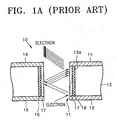
- FIG. 1A is a cross-section of a conventional electron amplifier 10.
- the conventional electron amplifier 10 includes a substrate 13, electrode layers 14 and 15 formed on the upper and lower surfaces of the substrate 13, respectively, a through hole 11 formed perpendicular to the electron layers 14 and 15, a resistive layer 16 formed along the inner wall of the through hole 11, and an electron emission layer 17 formed covering the resistive layer 16.
- FIG. 1B illustrates a method of manufacturing a conventional electron amplifier.
- a core glass 22 which melts in a chemical etching solution and a lead glass 21 which does not melt in the chemical etching solution are prepared.
- the core glass 22 fits into the lead glass 21 to obtain a single glass pipe 23.
- the single glass pipe 23 is stretched to obtain a thin glass fiber 23' as shown in step (c).
- glass fibers 23' are tied into a hexagonal bundle 24 as shown in step (d).
- the hexagonal bundle is stretched out to obtain a thin hexagonal multiple fiber 25 as shown in step (e).
- hexagonal multiple fibers 25 are tied into a bundle 26, and the bundle 26 is then attached to a glass skin to be shaped as shown in step (f).
- the bundle 26 is then thinly cut to obtain a wafer 27 as shown in step (g).
- the surface of the wafer 27 is polished, and the core glass 22 of the glass fiber 23' is etched using an appropriate etching solution. Then, the resultant wafer 27 undergoes a chemical process for increasing the secondary electron emission property of the wall of the glass fiber 23' and is then reduced in a hydrogen-ambient baking furnace. During this reduction, lead oxide on the glass surface turns into conductive lead and water, and lead particles form lumps. If the temperature is high, lead particle lumping prevails over new lead particle formation. Thus, the resistance between two electrodes is not determined by lead particles but by the temperature in the baking furnace.
- an electrode is formed of Inconel or Nichrome on the baked wafer 27, thereby completing a microchannel plate.
- the electrical operation characteristics of electron amplifiers are usually determined by their resistance, which in turn is determined by the ratio of the length of a through hole to the diameter thereof. Accordingly, it is difficult for conventional electron amplifiers to obtain a desired electron emission efficiency, for example, an electron emission efficiency of 10 3 through 10 5 times as much as a primary electron emission efficiency.
- an electron amplifier including a substrate in which a plurality of through holes are formed, a resistive layer deposited on the sidewalls of the through holes, an electron emissive layer deposited on the resistive layer and including carbon nanotubes, and an electrode layer formed on each of the upper and lower sides of the substrate.
- the present invention provides an electron amplifier with an excellent secondary electron emission property, and a method of simply manufacturing an electron amplifier, by which large display device screens can be easily manufactured.
- a method of manufacturing an electron amplifier In the method, first, through holes are formed in a substrate. Next, a resistive layer is formed on the sidewalls of the through holes. Thereafter, carbon nanotubes are added to a sol-gel solution of a material with a high secondary electron emission coefficient. Then, an electron emissive layer is deposited on the resistive layer by dipping the substrate having the through holes and the resistive layer into the sol-gel solution. Then, the substrate on which the through holes, the resistive layer, and the electron emission layer are formed is baked. An electrode layer is then formed on each of the upper and lower sides of the substrate so as to be perpendicular to the through holes.
- the electron emissive layer is formed of any of oxide-based and fluoride-based materials having a high secondary electron emission coefficient.
- the oxide-based material is one of MgO, SiO 2 , and La 2 O 3
- the fluoride-based material is one of CaF 2 and MgF 2 .
- the substrate is formed of any material selected from the group consisting of any glass, any ceramic, Al 2 O 3 , Cu, and Si.
- a secondary electron emission film is formed by mixing carbon nanotubes with a material having a high secondary electron emission efficiency.
- the electron amplifier provides a high secondary electron emission efficiency. Also, because the electron amplifier is simply manufactured using a sol-gel method, large display device screens can be economically mass-produced.
- an electron amplifier according to an embodiment of the present invention includes a substrate 33, a plurality of through holes 32 formed in the substrate 33, a resistive layer 35 formed along the inner wall of each of the through holes 32, an electron emission layer 37 deposited on the resistive layer 35 and including carbon nanotubes 45, and upper and lower electrode layers 31 formed on the upper and lower sides of the substrate 33, respectively, so as to be perpendicular to the through holes 32.
- the substrate 33 is formed of glass, ceramic such as Al 2 O 3 , or metal such as Cu or Si.
- the resistive layer 35 is formed of metal oxide with sufficient resistance to prevent an electrical short-circuit of the upper and lower electrode layers 31, and allow electrons to be adequately supplied to the electron emission layer 37 against voltage received from a power source.
- the electron emission layer 37 is formed of the carbon nanotubes 45 together with an oxide-based or fluoride-based material having high secondary electron emission efficiency.
- a secondary electron emission coefficient denotes a ratio of the number of incident primary electrons to the number of emitted secondary electrons.
- the carbon nanotube 45 a nano-sized graphite surface rolled into a cylindrical shape, is known to have unique physical properties depending on its shape and size.
- SPM scanning probing microscopy
- the carbon nanotubes 45 used in an electron amplifier according to the present invention can be manufactured using an arc discharge method, a laser vaporization method, a plasma enhanced chemical vapor deposition (PECVD) method, a thermal chemical vapor deposition (TCVD) method, or a vapor phase growth method.
- PECVD plasma enhanced chemical vapor deposition
- TCVD thermal chemical vapor deposition
- examples of an oxide-like material include MgO, SiO 2 , and La 2 O 3
- examples of a fluoride-like material include MgF 2 and CaF 2 .
- the electron of atoms making up the surface of the electron emission layer 35 absorbs the kinetic energy of a primary electron, which is emitted from an external source, when the primary electron collides with the surface of the electron emission layer 35, and is then emitted from the surface of the electron emission layer 35 against a Coulomb attraction. Because the electron is emitted by the kinetic energy of the primary electron, the emitted outermost electron is called a secondary electron. As the secondary electron emission coefficient of the electron emission layer 35 increases, more secondary electrons are emitted. The number of secondary electrons emitted can be calculated from measured current because current depends on a consecutive flow of secondary electrons.
- FIGS. 3A through 3C are pictures of an electron amplifier according to an embodiment of the present invention.
- FIG. 3A shows the top surface of the electron amplifier according to an embodiment of the present invention.
- FIG. 3B is a magnified picture of circle A of FIG. 3A.
- FIG. 3C is a magnified picture of circle B of FIG. 3B.
- reference numeral 33 denotes a substrate made of alumina Al 2 O 3
- reference numeral 35 denotes a resistive layer made of CuAl 2 O 4
- reference numeral 37 denotes an electron emissive layer made of SiO 2 or MgO.
- FIGS. 4A through 4E and 5 illustrate a method of manufacturing an electron amplifier according to an embodiment of the present invention.
- a substrate 33 is formed of an alumina paste and then dried.
- the dried alumina substrate 33 is soft enough to easily form through holes 32 as shown in FIG. 4B.
- the substrate 33 with the through holes 32 is compressed into a thin plate, and a plurality of thin substrates 33 are piled on top of one another as shown in FIG. 4C. Thereafter, the piled substrates 33 are baked to form a basic structure 30 of an electron amplifier as shown in FIG. 4D.
- Cu or Ni is deposited on the basic structure 30 using electron beams, a sputtering (deposition) method, or a plating method, and then baked. Accordingly, CuAl 2 O 4 , CuO, or NiAl 2 O 4 flows along the inner walls of the through holes 32, thereby forming resistive layers 35 as shown in FIG. 4E.
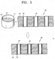
- FIG. 5 illustrates a process of forming an electron emissive film on the basic structure 30 completed through the steps of FIGS. 4A through 4E.
- a sol-gel solution of materials with an excellent secondary electron emission property for example, a SiO 2 or MgO sol-gel solution 43
- the carbon nanotubes 45 are dispersed in the sol-gel solution 43.
- the basic structure 30 completed in FIG. 4E is dipped in the sol-gel solution 43 and then baked for a short period of time at a low temperature. Accordingly, an electron emissive layer 37 including the carbon nanotubes 45 is formed along the surface of the resistive layer 35, thereby completing the fabrication of an electron amplifier 30' according to an embodiment of the present invention as shown in FIG. 2.
- FIG. 6 is a graph showing the emission characteristics of a secondary electron emissive film including carbon nanotubes used in an electron amplifier according to an embodiment of the present invention.
- Carbon nanotubes of 0.015g were dispersed in a solution mixed with 1, 3-propanediol (C 3 H 8 O 2 ), MgO acetate (MG(CH 3 CO 2 ) 2 ⁇ 4H 2 O), and MgO to obtain an 0.65M MgO solution.
- MG(CH 3 CO 2 ) 2 ⁇ 4H 2 O MgO acetate
- the secondary electron emission efficiency ( ⁇ ) represents how many secondary electrons are emitted when primary electrons collide with the silicon substrate on which the secondary electron emissive film is formed.
- the secondary electron emission efficiency ( ⁇ ) denotes a ratio of secondary electron current with respect to primary electron current. As shown in FIG. 6, when the net energy is 300 (eV), the highest secondary electron emission efficiency ( ⁇ ) is provided. Accordingly, the net energy at which the secondary electron emission efficiency is the highest, as in the above experiment, is used to provide a highly efficient electron amplifier.
- the electron amplifier according to an embodiment of the present invention can be simply manufactured at a low cost using the manufacturing method using a sol-gel solution. Also, a pure, uniform electron emissive layer can be obtained at a low temperature. Thus, the electron amplifier is suitable for large display device screens.
- the electron emissive layer is formed by adding carbon nanotubes to a material with an excellent secondary electron emission property, the electron emissive layer provides a significantly higher secondary electron emission efficiency than existing electron emissive layers.
Landscapes
- Chemical & Material Sciences (AREA)
- Engineering & Computer Science (AREA)
- Nanotechnology (AREA)
- Theoretical Computer Science (AREA)
- Physics & Mathematics (AREA)
- Crystallography & Structural Chemistry (AREA)
- Mathematical Physics (AREA)
- Organic Chemistry (AREA)
- Inorganic Chemistry (AREA)
- Electron Tubes For Measurement (AREA)
- Cathode-Ray Tubes And Fluorescent Screens For Display (AREA)
- Cold Cathode And The Manufacture (AREA)
- Common Detailed Techniques For Electron Tubes Or Discharge Tubes (AREA)
Abstract
An electron amplifier and a method of manufacturing the same are provided.
The electron amplifier includes a substrate (33) in which a plurality of through holes (32) are
formed, a resistive layer (35) deposited on the sidewalls of the through holes, an electron
emissive layer (37) including carbon nanotubes (45) which is deposited on the resistive layer,
and an electrode layer (31) formed on each of the upper and lower sides of the substrate.
Because the electron emissive layer of the electron amplifier is uniform and provides
a high electron emission efficiency, the electron amplification efficiency is improved.
The electron amplifier manufacturing method enables economical mass production
of electron amplifiers.
Description
- The present invention relates to an electron amplifier and a method of manufacturing the same, and more particularly, to an electron amplifier utilizing carbon nanotubes and a method of manufacturing the electron amplifier.
- Electron amplifiers include a secondary electron emission layer in order to induce emission of secondary electrons. Electron amplifiers are based on the principle that if primary electrons are accelerated to collide with the secondary electron emission layer, bound electrons on the surface of the secondary electron emission layer absorb the kinetic energy of the primary electrons, and are then emitted as secondary electrons.
- Electron amplifiers are generally used in measuring equipment, such as, mass analyzers, surface analyzers, energy analyzers, and the like, and are also used in night goggles, display devices, and the like.
- FIG. 1A is a cross-section of a
conventional electron amplifier 10. Referring to FIG. 1A, theconventional electron amplifier 10 includes asubstrate 13,electrode layers substrate 13, respectively, a throughhole 11 formed perpendicular to theelectron layers resistive layer 16 formed along the inner wall of the throughhole 11, and anelectron emission layer 17 formed covering theresistive layer 16. - FIG. 1B illustrates a method of manufacturing a conventional electron amplifier. As shown in step (a), a
core glass 22 which melts in a chemical etching solution and alead glass 21 which does not melt in the chemical etching solution are prepared. As shown in step (b), thecore glass 22 fits into thelead glass 21 to obtain asingle glass pipe 23. Thereafter, thesingle glass pipe 23 is stretched to obtain a thin glass fiber 23' as shown in step (c). Then, glass fibers 23' are tied into ahexagonal bundle 24 as shown in step (d). Next, the hexagonal bundle is stretched out to obtain a thin hexagonalmultiple fiber 25 as shown in step (e). Next, hexagonalmultiple fibers 25 are tied into abundle 26, and thebundle 26 is then attached to a glass skin to be shaped as shown in step (f). Thebundle 26 is then thinly cut to obtain awafer 27 as shown in step (g). - Next, the surface of the
wafer 27 is polished, and thecore glass 22 of the glass fiber 23' is etched using an appropriate etching solution. Then, theresultant wafer 27 undergoes a chemical process for increasing the secondary electron emission property of the wall of the glass fiber 23' and is then reduced in a hydrogen-ambient baking furnace. During this reduction, lead oxide on the glass surface turns into conductive lead and water, and lead particles form lumps. If the temperature is high, lead particle lumping prevails over new lead particle formation. Thus, the resistance between two electrodes is not determined by lead particles but by the temperature in the baking furnace. - Finally, an electrode is formed of Inconel or Nichrome on the
baked wafer 27, thereby completing a microchannel plate. - The electrical operation characteristics of electron amplifiers are usually determined by their resistance, which in turn is determined by the ratio of the length of a through hole to the diameter thereof. Accordingly, it is difficult for conventional electron amplifiers to obtain a desired electron emission efficiency, for example, an electron emission efficiency of 103 through 105 times as much as a primary electron emission efficiency.
- According to an aspect of the present invention, there is provided an electron amplifier including a substrate in which a plurality of through holes are formed, a resistive layer deposited on the sidewalls of the through holes, an electron emissive layer deposited on the resistive layer and including carbon nanotubes, and an electrode layer formed on each of the upper and lower sides of the substrate.
- The present invention provides an electron amplifier with an excellent secondary electron emission property, and a method of simply manufacturing an electron amplifier, by which large display device screens can be easily manufactured.
- According to another aspect of the present invention, there is provided a method of manufacturing an electron amplifier. In the method, first, through holes are formed in a substrate. Next, a resistive layer is formed on the sidewalls of the through holes. Thereafter, carbon nanotubes are added to a sol-gel solution of a material with a high secondary electron emission coefficient. Then, an electron emissive layer is deposited on the resistive layer by dipping the substrate having the through holes and the resistive layer into the sol-gel solution. Then, the substrate on which the through holes, the resistive layer, and the electron emission layer are formed is baked. An electrode layer is then formed on each of the upper and lower sides of the substrate so as to be perpendicular to the through holes.
- Preferably, the electron emissive layer is formed of any of oxide-based and fluoride-based materials having a high secondary electron emission coefficient.
- It is also preferable that the oxide-based material is one of MgO, SiO2, and La2O3, and the fluoride-based material is one of CaF2 and MgF2.
- Preferably, the substrate is formed of any material selected from the group consisting of any glass, any ceramic, Al2O3, Cu, and Si.
- In the electron amplifier according to the present invention, a secondary electron emission film is formed by mixing carbon nanotubes with a material having a high secondary electron emission efficiency. Thus, the electron amplifier provides a high secondary electron emission efficiency. Also, because the electron amplifier is simply manufactured using a sol-gel method, large display device screens can be economically mass-produced.
- The above and other features and advantages of the present invention will become more apparent by describing in detail exemplary embodiments thereof with reference to the attached drawings in which:
- FIG. 1A is a cross-section of a conventional electron amplifier;
- FIG. 1 B illustrates a method of manufacturing a conventional electron amplifier;
- FIG. 2 is a perspective view of an electron amplifier according to an embodiment of the present invention;
- FIG. 3A is a plan view of an electron amplifier according to an embodiment of the present invention;
- FIG. 3B is a magnified view of circle A of FIG. 3A;
- FIG. 3C is a magnified view of circle B of FIG. 3B;
- FIGS. 4A through 4E illustrate steps before an electron emission film deposition step in a method of manufacturing an electron amplifier according to an embodiment of the present invention;
- FIG. 5 illustrates the electron emission film deposition step in the method of manufacturing the electron amplifier according to an embodiment of the present invention; and
- FIG. 6 is a graph of secondary electron emission efficiency (δ) versus net energy of primary electrons of a secondary electron emission film installed in an electron amplifier according to an embodiment of the present invention.
-
- The present invention will now be described more fully with reference to the accompanying drawings, in which preferred embodiments of the invention are shown. Throughout the drawings, the same reference numerals denote the same members.
- Referring to FIG. 2, an electron amplifier according to an embodiment of the present invention includes a
substrate 33, a plurality of throughholes 32 formed in thesubstrate 33, aresistive layer 35 formed along the inner wall of each of the throughholes 32, anelectron emission layer 37 deposited on theresistive layer 35 and includingcarbon nanotubes 45, and upper and lower electrode layers 31 formed on the upper and lower sides of thesubstrate 33, respectively, so as to be perpendicular to the throughholes 32. - The
substrate 33 is formed of glass, ceramic such as Al2O3, or metal such as Cu or Si. - The
resistive layer 35 is formed of metal oxide with sufficient resistance to prevent an electrical short-circuit of the upper and lower electrode layers 31, and allow electrons to be adequately supplied to theelectron emission layer 37 against voltage received from a power source. - The
electron emission layer 37 is formed of thecarbon nanotubes 45 together with an oxide-based or fluoride-based material having high secondary electron emission efficiency. A secondary electron emission coefficient denotes a ratio of the number of incident primary electrons to the number of emitted secondary electrons. - The
carbon nanotube 45, a nano-sized graphite surface rolled into a cylindrical shape, is known to have unique physical properties depending on its shape and size. Frank reported in 1998 that, according to a scanning probing microscopy (SPM) measurement of the conductivity of a carbon nano fiber dipped in a liquid, carbon nanotubes exhibit quantum behaviour and have remarkably high conductivity. Carbon nanotubes have been observed to provide a stable current density of 107A/cm2 or greater by Frank et al. and a stable current density of 1013A/cm2 or greater by Avoris et al. - Because of the excellent electrical characteristics of carbon nanotubes, the manufacture of display devices, electron guns, lithium batteries, and transistors, using the electron emission property of carbon nanotubes, has been actively studied of late.
- The
carbon nanotubes 45 used in an electron amplifier according to the present invention can be manufactured using an arc discharge method, a laser vaporization method, a plasma enhanced chemical vapor deposition (PECVD) method, a thermal chemical vapor deposition (TCVD) method, or a vapor phase growth method. - Among materials with a high secondary electron emission coefficient to form the
electron emission layer 35, examples of an oxide-like material include MgO, SiO2, and La2O3, and examples of a fluoride-like material include MgF2 and CaF2. - The electron of atoms making up the surface of the
electron emission layer 35 absorbs the kinetic energy of a primary electron, which is emitted from an external source, when the primary electron collides with the surface of theelectron emission layer 35, and is then emitted from the surface of theelectron emission layer 35 against a Coulomb attraction. Because the electron is emitted by the kinetic energy of the primary electron, the emitted outermost electron is called a secondary electron. As the secondary electron emission coefficient of theelectron emission layer 35 increases, more secondary electrons are emitted. The number of secondary electrons emitted can be calculated from measured current because current depends on a consecutive flow of secondary electrons. - FIGS. 3A through 3C are pictures of an electron amplifier according to an embodiment of the present invention. FIG. 3A shows the top surface of the electron amplifier according to an embodiment of the present invention. FIG. 3B is a magnified picture of circle A of FIG. 3A. FIG. 3C is a magnified picture of circle B of FIG. 3B. In FIG. 3C,
reference numeral 33 denotes a substrate made of alumina Al2O3,reference numeral 35 denotes a resistive layer made of CuAl2O4, andreference numeral 37 denotes an electron emissive layer made of SiO2 or MgO. - FIGS. 4A through 4E and 5 illustrate a method of manufacturing an electron amplifier according to an embodiment of the present invention. First, as shown in FIG. 4A, a
substrate 33 is formed of an alumina paste and then dried. The driedalumina substrate 33 is soft enough to easily form throughholes 32 as shown in FIG. 4B. - Next, the
substrate 33 with the throughholes 32 is compressed into a thin plate, and a plurality ofthin substrates 33 are piled on top of one another as shown in FIG. 4C. Thereafter, the piledsubstrates 33 are baked to form abasic structure 30 of an electron amplifier as shown in FIG. 4D. - Then, Cu or Ni is deposited on the
basic structure 30 using electron beams, a sputtering (deposition) method, or a plating method, and then baked. Accordingly, CuAl2O4, CuO, or NiAl2O4 flows along the inner walls of the throughholes 32, thereby formingresistive layers 35 as shown in FIG. 4E. - FIG. 5 illustrates a process of forming an electron emissive film on the
basic structure 30 completed through the steps of FIGS. 4A through 4E. Referring to FIG. 5, a sol-gel solution of materials with an excellent secondary electron emission property, for example, a SiO2 or MgO sol-gel solution 43, is stored in avessel 41, and thecarbon nanotubes 45 are dispersed in the sol-gel solution 43. Thebasic structure 30 completed in FIG. 4E is dipped in the sol-gel solution 43 and then baked for a short period of time at a low temperature. Accordingly, an electronemissive layer 37 including thecarbon nanotubes 45 is formed along the surface of theresistive layer 35, thereby completing the fabrication of an electron amplifier 30' according to an embodiment of the present invention as shown in FIG. 2. - FIG. 6 is a graph showing the emission characteristics of a secondary electron emissive film including carbon nanotubes used in an electron amplifier according to an embodiment of the present invention. Carbon nanotubes of 0.015g were dispersed in a solution mixed with 1, 3-propanediol (C3H8O2), MgO acetate (MG(CH3CO2)2□4H2O), and MgO to obtain an 0.65M MgO solution. Then, a secondary electron emissive film was coated on a silicon substrate using the above-described manufacturing method. The graph of FIG. 6 shows secondary electron emission efficiency (δ) versus the net energy of the primary electrons, that is, energy corresponding to the difference between a primary electron energy (Ep) and a bias potential. Here, the secondary electron emission efficiency (δ) represents how many secondary electrons are emitted when primary electrons collide with the silicon substrate on which the secondary electron emissive film is formed.
- The secondary electron emission efficiency (δ) denotes a ratio of secondary electron current with respect to primary electron current. As shown in FIG. 6, when the net energy is 300 (eV), the highest secondary electron emission efficiency (δ) is provided. Accordingly, the net energy at which the secondary electron emission efficiency is the highest, as in the above experiment, is used to provide a highly efficient electron amplifier.
- The electron amplifier according to an embodiment of the present invention can be simply manufactured at a low cost using the manufacturing method using a sol-gel solution. Also, a pure, uniform electron emissive layer can be obtained at a low temperature. Thus, the electron amplifier is suitable for large display device screens. In particular, because the electron emissive layer is formed by adding carbon nanotubes to a material with an excellent secondary electron emission property, the electron emissive layer provides a significantly higher secondary electron emission efficiency than existing electron emissive layers.
- Because of these improved electron emission characteristics, a desired secondary electron emission efficiency can be obtained without having to increase the primary electron current or adjust the dimensions of the through holes. Thus, a limit in the ratio of the length of a through hole to the diameter thereof is overcome, which facilitates more control over an electrical performance in the manufacture of an electron amplifier.
- While the present invention has been particularly shown and described with reference to exemplary embodiments thereof, it will be understood by those of ordinary skill in the art that various changes in form and details may be made therein without departing from the spirit and scope of the present invention as defined by the following claims. For example, other materials with an excellent secondary electron emission efficiency, not mentioned herein, can be used to fabricate an electron amplifier according to the present invention.
Claims (10)
- An electron amplifier comprising:a substrate in which a plurality of through holes are formed;a resistive layer deposited on the sidewalls of the through holes;an electron emissive layer deposited on the resistive layer and including carbon nanotubes; andan electrode layer formed on each of the upper and lower sides of the substrate.
- The electron amplifier of claim 1, wherein the electron emissive layer is formed of any of oxide-based and fluoride-based materials having a high secondary electron emission coefficient.
- The electron amplifier of claim 2, wherein the electron emissive layer is of oxide-based material being one of MgO, SiO2, and La2O3.
- The electron amplifier of claim 2, wherein the electron emissive layer is of fluoride-based material being one of CaF2 and MgF2.
- The electron amplifier of any preceding claim, wherein the substrate is formed of any material selected from the group consisting of any glass, any ceramic, Al2O3, Cu, and Si.
- A method of manufacturing an electron amplifier, the method comprising the steps of:(a) forming through holes in a substrate;(b) depositing a resistive layer on the sidewalls of the through holes;(c) adding carbon nanotubes to a sol-gel solution of a material with a high secondary electron emission coefficient;(d) depositing an electron emissive layer on the resistive layer by dipping the substrate having the through holes and the resistive layer into the sol-gel solution;(e) baking the substrate on which the through holes, the resistive layer, and the electron emission layer are formed; and(f) forming an electrode layer on each of the upper and lower sides of the substrate so as to be perpendicular to the through holes.
- The method of claim 6, wherein the electron emissive layer is formed of any of oxide-based and fluoride-based materials having a high secondary electron emission coefficient.
- The method of claim 7, wherein the electron emissive layer is of oxide-based material being one of MgO, SiO2, and La2O3.
- The method of claim 7, wherein the electron emissive layer is of fluoride-based material being one of CaF2 and MgF2.
- The method of any of claims 6 to 9, wherein the substrate is formed of any material selected from the group consisting of any glass, any ceramic, Al2O3, Cu, and Si.
Applications Claiming Priority (2)
| Application Number | Priority Date | Filing Date | Title |
|---|---|---|---|
| KR1020020009088A KR100873634B1 (en) | 2002-02-20 | 2002-02-20 | Electronic amplifier including carbon nanotube and manufacturing method |
| KR2002009088 | 2002-02-20 |
Publications (1)
| Publication Number | Publication Date |
|---|---|
| EP1339087A1 true EP1339087A1 (en) | 2003-08-27 |
Family
ID=27656450
Family Applications (1)
| Application Number | Title | Priority Date | Filing Date |
|---|---|---|---|
| EP03251034A Withdrawn EP1339087A1 (en) | 2002-02-20 | 2003-02-20 | Electron amplifier utilizing carbon nanotubes and method of manufacturing the same |
Country Status (4)
| Country | Link |
|---|---|
| US (2) | US6870308B2 (en) |
| EP (1) | EP1339087A1 (en) |
| JP (1) | JP2003257359A (en) |
| KR (1) | KR100873634B1 (en) |
Cited By (3)
| Publication number | Priority date | Publication date | Assignee | Title |
|---|---|---|---|---|
| FR2880200A1 (en) * | 2004-12-24 | 2006-06-30 | St Microelectronics Sa | PLATE HAVING TRANSVERSE CONDUCTORS AND APPLICATION TO A FUEL CELL |
| CN103413642A (en) * | 2013-08-26 | 2013-11-27 | 四川永星电子有限公司 | Novel chip resistor and chip resistor installation body |
| US9064676B2 (en) | 2008-06-20 | 2015-06-23 | Arradiance, Inc. | Microchannel plate devices with tunable conductive films |
Families Citing this family (32)
| Publication number | Priority date | Publication date | Assignee | Title |
|---|---|---|---|---|
| WO2004027336A1 (en) * | 2002-09-17 | 2004-04-01 | Midwest Research Institute | Carbon nanotube heat-exchange systems |
| US7126263B2 (en) * | 2003-12-03 | 2006-10-24 | Itt Manufacturing Enterprises Inc. | Perforated mega-boule wafer for fabrication of microchannel plates (MCPs) |
| US7109644B2 (en) * | 2003-12-03 | 2006-09-19 | Itt Manufacturing Enterprises, Inc. | Device and method for fabrication of microchannel plates using a mega-boule wafer |
| KR20050072987A (en) * | 2004-01-08 | 2005-07-13 | 삼성전자주식회사 | Surface light source device and liquid crystal display apparatus having the same |
| US7947371B2 (en) * | 2004-11-05 | 2011-05-24 | E. I. Du Pont De Nemours And Company | Single-walled carbon nanotube composites |
| KR101082437B1 (en) | 2005-03-02 | 2011-11-11 | 삼성에스디아이 주식회사 | An electron emission source, a preparing method thereof, and an electron emission device using the same |
| GB0512001D0 (en) * | 2005-06-13 | 2005-07-20 | Council Cent Lab Res Councils | Electron amplifier device |
| US7858918B2 (en) * | 2007-02-05 | 2010-12-28 | Ludwig Lester F | Molecular transistor circuits compatible with carbon nanotube sensors and transducers |
| US7838809B2 (en) | 2007-02-17 | 2010-11-23 | Ludwig Lester F | Nanoelectronic differential amplifiers and related circuits having carbon nanotubes, graphene nanoribbons, or other related materials |
| US20090001820A1 (en) * | 2007-06-26 | 2009-01-01 | George Dewberry | Electrical line conditioner |
| US20090001811A1 (en) * | 2007-06-26 | 2009-01-01 | George Dewberry | Electrical line conditioner |
| RU2364981C1 (en) * | 2007-12-05 | 2009-08-20 | ФГУП "НИИ физических проблем им. Ф.В. Лукина" | Amplifier-convertor |
| US8052884B2 (en) * | 2008-02-27 | 2011-11-08 | Arradiance, Inc. | Method of fabricating microchannel plate devices with multiple emissive layers |
| US7855493B2 (en) * | 2008-02-27 | 2010-12-21 | Arradiance, Inc. | Microchannel plate devices with multiple emissive layers |
| KR100967024B1 (en) * | 2008-04-14 | 2010-06-30 | 삼성전기주식회사 | Probe substrate manufacturing method |
| US8237129B2 (en) * | 2008-06-20 | 2012-08-07 | Arradiance, Inc. | Microchannel plate devices with tunable resistive films |
| US8101913B2 (en) * | 2009-09-11 | 2012-01-24 | Ut-Battelle, Llc | Method of making large area conformable shape structures for detector/sensor applications using glass drawing technique and postprocessing |
| CA2684811C (en) * | 2009-11-06 | 2017-05-23 | Bubble Technology Industries Inc. | Microstructure photomultiplier assembly |
| KR101711145B1 (en) * | 2010-09-03 | 2017-03-13 | 삼성전자주식회사 | Portable quadrupole ion trap mass spectrometer |
| FR2964785B1 (en) * | 2010-09-13 | 2013-08-16 | Photonis France | ELECTRON MULTIPLIER DEVICE WITH NANODIAMANT LAYER. |
| JP5948249B2 (en) * | 2010-12-01 | 2016-07-06 | Hoya株式会社 | Method for manufacturing substrate for electronic amplifier, method for manufacturing electronic amplifier, and method for manufacturing radiation detector |
| JP5855577B2 (en) * | 2010-12-01 | 2016-02-09 | Hoya株式会社 | Method for manufacturing substrate for electronic amplifier, method for manufacturing electronic amplifier, and method for manufacturing radiation detector |
| CN105244246B (en) * | 2014-07-10 | 2017-06-06 | 清华大学 | Field-transmitting cathode and field emission apparatus |
| CN105448624B (en) | 2014-07-10 | 2017-09-01 | 清华大学 | The preparation method of field-transmitting cathode |
| JP6496217B2 (en) * | 2015-09-04 | 2019-04-03 | 浜松ホトニクス株式会社 | Microchannel plate and electron multiplier |
| JP6340102B1 (en) * | 2017-03-01 | 2018-06-06 | 浜松ホトニクス株式会社 | Microchannel plate and electron multiplier |
| KR102283035B1 (en) * | 2017-07-06 | 2021-07-28 | (주) 브이에스아이 | Electronically amplified compact x-ray tube |
| KR102283038B1 (en) * | 2017-08-03 | 2021-07-28 | (주) 브이에스아이 | X-ray tube |
| KR102389448B1 (en) * | 2017-08-16 | 2022-04-22 | (주) 브이에스아이 | X-ray tube having a micro channel plate |
| KR102292412B1 (en) * | 2018-08-02 | 2021-08-23 | (주) 브이에스아이 | Micro focus x-ray tube |
| RU2692094C1 (en) * | 2018-12-26 | 2019-06-21 | Федеральное государственное автономное образовательное учреждение высшего образования "Национальный исследовательский университет "Московский институт электронной техники" | Planar two-spectral photoelectronic multiplier |
| CN114646689B (en) * | 2020-12-17 | 2025-07-22 | 清华大学 | Secondary electron probe and secondary electron detector |
Citations (3)
| Publication number | Priority date | Publication date | Assignee | Title |
|---|---|---|---|---|
| EP1122759A2 (en) | 2000-02-07 | 2001-08-08 | Samsung SDI Co., Ltd. | Secondary electron amplification structure employing carbon nanotube, and plasma panel and back light using the same |
| EP1253614A1 (en) * | 2000-01-17 | 2002-10-30 | Hamamatsu Photonics K. K. | Cathode for emitting photoelectron or secondary electron, photomultiplier tube, and electron-multiplier tube |
| US20020167254A1 (en) * | 2001-05-14 | 2002-11-14 | Craig Richard A. | Acicular photomultiplier photocathode structure |
Family Cites Families (10)
| Publication number | Priority date | Publication date | Assignee | Title |
|---|---|---|---|---|
| US3911167A (en) * | 1970-05-01 | 1975-10-07 | Texas Instruments Inc | Electron multiplier and method of making same |
| IL42668A (en) * | 1973-07-05 | 1976-02-29 | Seidman A | Channel electron multipliers |
| US4825118A (en) * | 1985-09-06 | 1989-04-25 | Hamamatsu Photonics Kabushiki Kaisha | Electron multiplier device |
| US5086248A (en) * | 1989-08-18 | 1992-02-04 | Galileo Electro-Optics Corporation | Microchannel electron multipliers |
| DE69030145T2 (en) * | 1989-08-18 | 1997-07-10 | Galileo Electro Optics Corp | Continuous thin film dynodes |
| JPH06176734A (en) * | 1991-07-24 | 1994-06-24 | Yukiro Takahashi | Electron multiplier element |
| US5729244A (en) * | 1995-04-04 | 1998-03-17 | Lockwood; Harry F. | Field emission device with microchannel gain element |
| KR100496281B1 (en) * | 2000-02-07 | 2005-06-17 | 삼성에스디아이 주식회사 | Micro channel plate applying secondary electron amplification structure and field emission display using the same |
| KR20010090256A (en) * | 2000-03-24 | 2001-10-18 | 김순택 | Elecrton amplier and method of manufacturing the same |
| US6657385B2 (en) * | 2000-06-20 | 2003-12-02 | Burle Technologies, Inc. | Diamond transmission dynode and photomultiplier or imaging device using same |
-
2002
- 2002-02-20 KR KR1020020009088A patent/KR100873634B1/en not_active Expired - Fee Related
-
2003
- 2003-02-20 JP JP2003041994A patent/JP2003257359A/en active Pending
- 2003-02-20 EP EP03251034A patent/EP1339087A1/en not_active Withdrawn
- 2003-02-20 US US10/368,466 patent/US6870308B2/en not_active Expired - Fee Related
-
2005
- 2005-02-04 US US11/049,898 patent/US7025652B2/en not_active Expired - Fee Related
Patent Citations (3)
| Publication number | Priority date | Publication date | Assignee | Title |
|---|---|---|---|---|
| EP1253614A1 (en) * | 2000-01-17 | 2002-10-30 | Hamamatsu Photonics K. K. | Cathode for emitting photoelectron or secondary electron, photomultiplier tube, and electron-multiplier tube |
| EP1122759A2 (en) | 2000-02-07 | 2001-08-08 | Samsung SDI Co., Ltd. | Secondary electron amplification structure employing carbon nanotube, and plasma panel and back light using the same |
| US20020167254A1 (en) * | 2001-05-14 | 2002-11-14 | Craig Richard A. | Acicular photomultiplier photocathode structure |
Non-Patent Citations (2)
| Title |
|---|
| YI ET AL.: "A microchannel plate for a high-efficiency field emission display", APPLIED PHYSICS LETTERS, vol. 77, no. 11, 2000, XP012026137, DOI: doi:10.1063/1.1309025 |
| YI W ET AL: "MOCROCHANNEL PLATE FOR HIGH-EFFICIENCY FIELD EMISSION DISPLAY", APPLIED PHYSICS LETTERS, AMERICAN INSTITUTE OF PHYSICS. NEW YORK, US, VOL. 77, NR. 11, PAGE(S) 1716-1718, ISSN: 0003-6951, XP000964194 * |
Cited By (6)
| Publication number | Priority date | Publication date | Assignee | Title |
|---|---|---|---|---|
| FR2880200A1 (en) * | 2004-12-24 | 2006-06-30 | St Microelectronics Sa | PLATE HAVING TRANSVERSE CONDUCTORS AND APPLICATION TO A FUEL CELL |
| US7993796B2 (en) | 2004-12-24 | 2011-08-09 | Stmicroelectronics Sa | Wafer provided with transverse conductors and application to a fuel cell |
| US9064676B2 (en) | 2008-06-20 | 2015-06-23 | Arradiance, Inc. | Microchannel plate devices with tunable conductive films |
| US9368332B2 (en) | 2008-06-20 | 2016-06-14 | Arradiance, Llc | Microchannel plate devices with tunable resistive films |
| CN103413642A (en) * | 2013-08-26 | 2013-11-27 | 四川永星电子有限公司 | Novel chip resistor and chip resistor installation body |
| CN103413642B (en) * | 2013-08-26 | 2015-12-09 | 四川永星电子有限公司 | A kind of Novel patch resistor and patch resistor fixing body |
Also Published As
| Publication number | Publication date |
|---|---|
| US20030173884A1 (en) | 2003-09-18 |
| US20050200254A1 (en) | 2005-09-15 |
| KR100873634B1 (en) | 2008-12-12 |
| US6870308B2 (en) | 2005-03-22 |
| US7025652B2 (en) | 2006-04-11 |
| JP2003257359A (en) | 2003-09-12 |
| KR20030069450A (en) | 2003-08-27 |
Similar Documents
| Publication | Publication Date | Title |
|---|---|---|
| US7025652B2 (en) | Electron amplifier utilizing carbon nanotubes and method of manufacturing the same | |
| KR100649369B1 (en) | Graphite nanofibers, electron-emitting source and method for preparing the same, display element equipped with the electron-emitting source as well as lithium ion secondary battery | |
| CN100473602C (en) | Carbon-nano tube structure, method of manufacturing the same, and field emitter and display device each adopting the same | |
| US7081030B2 (en) | Method for making a carbon nanotube-based field emission display | |
| Guillorn et al. | Self-aligned gated field emission devices using single carbon nanofiber cathodes | |
| US7501146B2 (en) | Carbon nanotube emitter and its fabrication method and field emission device (FED) using the carbon nanotube emitter and its fabrication method | |
| WO1998050604A1 (en) | Silicon etching process for making microchannel plates | |
| WO2014025615A1 (en) | Methods for graphene fabrication on patterned catalytic metal | |
| Lim et al. | Enhanced field emission properties of carbon nanotube bundles confined in SiO2 pits | |
| US7221087B2 (en) | Carbon nanotube-based field emission display | |
| US6812635B2 (en) | Cathode for field emission device | |
| JP2006054162A (en) | Dielectric device | |
| US7573200B2 (en) | Plasma display panel | |
| JP2006236965A (en) | Electron emitting element | |
| JPH01107440A (en) | Electron emission element | |
| JP2006236964A (en) | Electron emitting element | |
| EP2126954A1 (en) | Field emission device with anode coating | |
| US20020117960A1 (en) | Field emission wafer and process for making same for use in field emission display devices | |
| KR100668332B1 (en) | Method for manufacturing a device with carbide and nitride nanoelectronic emitters | |
| EP1251543A1 (en) | Vacuum power switches | |
| JP3397236B2 (en) | Method of manufacturing field emission device | |
| KR20010055227A (en) | Field Emission Device Using Carbon Nanotube And Fabrication Method Thereof | |
| KR100322611B1 (en) | Fabrication Method of Field Emission Device Using Carbon Nanotube | |
| KR20010057163A (en) | Field emission device and fabricating method thereof | |
| JP2002170479A (en) | Cathode of electron tube |
Legal Events
| Date | Code | Title | Description |
|---|---|---|---|
| PUAI | Public reference made under article 153(3) epc to a published international application that has entered the european phase |
Free format text: ORIGINAL CODE: 0009012 |
|
| AK | Designated contracting states |
Designated state(s): AT BE BG CH CY CZ DE DK EE ES FI FR GB GR HU IE IT LI LU MC NL PT SE SI SK TR |
|
| AX | Request for extension of the european patent |
Extension state: AL LT LV MK RO |
|
| 17P | Request for examination filed |
Effective date: 20040121 |
|
| AKX | Designation fees paid |
Designated state(s): DE FR GB |
|
| 17Q | First examination report despatched |
Effective date: 20080404 |
|
| STAA | Information on the status of an ep patent application or granted ep patent |
Free format text: STATUS: THE APPLICATION IS DEEMED TO BE WITHDRAWN |
|
| 18D | Application deemed to be withdrawn |
Effective date: 20100901 |