EP1339054A1 - Optical record medium and its manufacturing method, and injection molding machine - Google Patents
Optical record medium and its manufacturing method, and injection molding machine Download PDFInfo
- Publication number
- EP1339054A1 EP1339054A1 EP01998969A EP01998969A EP1339054A1 EP 1339054 A1 EP1339054 A1 EP 1339054A1 EP 01998969 A EP01998969 A EP 01998969A EP 01998969 A EP01998969 A EP 01998969A EP 1339054 A1 EP1339054 A1 EP 1339054A1
- Authority
- EP
- European Patent Office
- Prior art keywords
- substrate
- light transmitting
- recording medium
- optical recording
- medium according
- Prior art date
- Legal status (The legal status is an assumption and is not a legal conclusion. Google has not performed a legal analysis and makes no representation as to the accuracy of the status listed.)
- Withdrawn
Links
Images





Classifications
-
- G—PHYSICS
- G11—INFORMATION STORAGE
- G11B—INFORMATION STORAGE BASED ON RELATIVE MOVEMENT BETWEEN RECORD CARRIER AND TRANSDUCER
- G11B7/00—Recording or reproducing by optical means, e.g. recording using a thermal beam of optical radiation by modifying optical properties or the physical structure, reproducing using an optical beam at lower power by sensing optical properties; Record carriers therefor
- G11B7/24—Record carriers characterised by shape, structure or physical properties, or by the selection of the material
- G11B7/24018—Laminated discs
- G11B7/24027—Layers; Shape, structure or physical properties thereof
-
- G—PHYSICS
- G11—INFORMATION STORAGE
- G11B—INFORMATION STORAGE BASED ON RELATIVE MOVEMENT BETWEEN RECORD CARRIER AND TRANSDUCER
- G11B7/00—Recording or reproducing by optical means, e.g. recording using a thermal beam of optical radiation by modifying optical properties or the physical structure, reproducing using an optical beam at lower power by sensing optical properties; Record carriers therefor
- G11B7/24—Record carriers characterised by shape, structure or physical properties, or by the selection of the material
- G11B7/26—Apparatus or processes specially adapted for the manufacture of record carriers
- G11B7/263—Preparing and using a stamper, e.g. pressing or injection molding substrates
-
- B—PERFORMING OPERATIONS; TRANSPORTING
- B29—WORKING OF PLASTICS; WORKING OF SUBSTANCES IN A PLASTIC STATE IN GENERAL
- B29C—SHAPING OR JOINING OF PLASTICS; SHAPING OF MATERIAL IN A PLASTIC STATE, NOT OTHERWISE PROVIDED FOR; AFTER-TREATMENT OF THE SHAPED PRODUCTS, e.g. REPAIRING
- B29C45/00—Injection moulding, i.e. forcing the required volume of moulding material through a nozzle into a closed mould; Apparatus therefor
- B29C45/17—Component parts, details or accessories; Auxiliary operations
- B29C45/26—Moulds
- B29C45/263—Moulds with mould wall parts provided with fine grooves or impressions, e.g. for record discs
-
- B—PERFORMING OPERATIONS; TRANSPORTING
- B29—WORKING OF PLASTICS; WORKING OF SUBSTANCES IN A PLASTIC STATE IN GENERAL
- B29C—SHAPING OR JOINING OF PLASTICS; SHAPING OF MATERIAL IN A PLASTIC STATE, NOT OTHERWISE PROVIDED FOR; AFTER-TREATMENT OF THE SHAPED PRODUCTS, e.g. REPAIRING
- B29C45/00—Injection moulding, i.e. forcing the required volume of moulding material through a nozzle into a closed mould; Apparatus therefor
- B29C45/17—Component parts, details or accessories; Auxiliary operations
- B29C45/26—Moulds
- B29C45/263—Moulds with mould wall parts provided with fine grooves or impressions, e.g. for record discs
- B29C45/2632—Stampers; Mountings thereof
-
- B—PERFORMING OPERATIONS; TRANSPORTING
- B29—WORKING OF PLASTICS; WORKING OF SUBSTANCES IN A PLASTIC STATE IN GENERAL
- B29D—PRODUCING PARTICULAR ARTICLES FROM PLASTICS OR FROM SUBSTANCES IN A PLASTIC STATE
- B29D17/00—Producing carriers of records containing fine grooves or impressions, e.g. disc records for needle playback, cylinder records; Producing record discs from master stencils
- B29D17/005—Producing optically read record carriers, e.g. optical discs
-
- G—PHYSICS
- G11—INFORMATION STORAGE
- G11B—INFORMATION STORAGE BASED ON RELATIVE MOVEMENT BETWEEN RECORD CARRIER AND TRANSDUCER
- G11B23/00—Record carriers not specific to the method of recording or reproducing; Accessories, e.g. containers, specially adapted for co-operation with the recording or reproducing apparatus ; Intermediate mediums; Apparatus or processes specially adapted for their manufacture
- G11B23/0014—Record carriers not specific to the method of recording or reproducing; Accessories, e.g. containers, specially adapted for co-operation with the recording or reproducing apparatus ; Intermediate mediums; Apparatus or processes specially adapted for their manufacture record carriers not specifically of filamentary or web form
- G11B23/0021—Record carriers not specific to the method of recording or reproducing; Accessories, e.g. containers, specially adapted for co-operation with the recording or reproducing apparatus ; Intermediate mediums; Apparatus or processes specially adapted for their manufacture record carriers not specifically of filamentary or web form discs
- G11B23/0028—Details
- G11B23/0035—Details means incorporated in the disc, e.g. hub, to enable its guiding, loading or driving
-
- G—PHYSICS
- G11—INFORMATION STORAGE
- G11B—INFORMATION STORAGE BASED ON RELATIVE MOVEMENT BETWEEN RECORD CARRIER AND TRANSDUCER
- G11B7/00—Recording or reproducing by optical means, e.g. recording using a thermal beam of optical radiation by modifying optical properties or the physical structure, reproducing using an optical beam at lower power by sensing optical properties; Record carriers therefor
- G11B7/24—Record carriers characterised by shape, structure or physical properties, or by the selection of the material
- G11B7/2403—Layers; Shape, structure or physical properties thereof
- G11B7/24047—Substrates
-
- G—PHYSICS
- G11—INFORMATION STORAGE
- G11B—INFORMATION STORAGE BASED ON RELATIVE MOVEMENT BETWEEN RECORD CARRIER AND TRANSDUCER
- G11B7/00—Recording or reproducing by optical means, e.g. recording using a thermal beam of optical radiation by modifying optical properties or the physical structure, reproducing using an optical beam at lower power by sensing optical properties; Record carriers therefor
- G11B7/24—Record carriers characterised by shape, structure or physical properties, or by the selection of the material
- G11B7/26—Apparatus or processes specially adapted for the manufacture of record carriers
Definitions
- the invention relates to an optical recording medium, its manufacturing method, and an injection molding apparatus. More particularly, the invention is suitable when it is applied to an optical recording medium onto/from which an information signal is recorded and reproduced by irradiating light from the side of a substrate where an information signal portion has been formed.
- optical information recording system it has an advantage such that the recording and reproduction can be performed in a contactless manner and a recording density which is one or more digits higher than that of a magnetic recording system can be accomplished.
- the optical information recording system also has an advantage such that it can cope with various memory formats such as read only type, write once type, rewritable type, and the like. Therefore, as a system which enables a cheap file of a large capacity to be realized, its application to fields of a wide range from the industrial use to the consumer use is considered.
- optical discs corresponding to the memory format of the read only type particularly, as optical discs corresponding to the memory format of the read only type, a digital audio disc (DAD), an optical video disc, and the like have widely been spread.
- DAD digital audio disc
- optical video disc and the like have widely been spread.
- a construction of the optical disc such as a digital audio disc or the like as mentioned above will be described hereinbelow. That is. in the optical disc, a reflective layer made of a thin metal film such as an aluminum (Al) film or the' like and a protective film to protect the reflective layer from moisture (H 2 O) or oxygen (O 2 ) in the atmosphere are sequentially formed on one principal plane of an optical disc substrate made of a transparent substrate on which concave/convex patterns such as pits, grooves, and the like showing an information signal have been formed.
- reproducing light such as a laser beam or the like is irradiated to the concave/convex patterns from the disc substrate side.
- the information signal is detected by a difference of reflectance between incident light and return light of the reproducing light.
- the disc substrate constructing such an optical disc is made of a synthetic resin material and molded by using a die apparatus for injection molding.
- a disc substrate molding injection molding apparatus for molding the disc substrate will now be described with reference to the drawings.
- the injection molding apparatus for molding the disc substrate is constructed by having a die 103 in which a fixed die 101 and a movable die 102 which are fixed to a stationary platen 100 are arranged so as to face each other.
- a cavity 104 for molding is formed between the fixed die 101 and the movable die 102.
- the cavity 104 for molding has a shape corresponding to a disc substrate 201 which is molded as shown in Fig. 17.
- a through-hole is formed at a center position of the fixed die 101 in the injection molding apparatus shown in Fig. 16.
- a stamper holder supporting member 106 having almost a ring shape pierces the through-hole.
- a sprue bush 107 is provided so as to be inserted into the stamper holder supporting member 106.
- the sprue bush 107 has the ring shape and a resin injection hole 108 is formed along a center axis in the ring shape.
- the resin injection hole 108 is constructed so that a synthetic resin material such as a fused polycarbonate resin or the like which is supplied from an injecting apparatus (not shown) can flow into the cavity 104 for molding. That is, a front edge side of the sprue bush 107 is constructed so as to face the inside of the cavity 104 for molding. A diameter of a front edge side of the stamper holder supporting member 106 which faces the cavity 104 for molding is reduced in a stairway manner.
- a stamper 109 is attached to a surface portion of the fixed die 101 constructing the cavity 104 for molding, that is, a surface portion of the fixed die 101 which faces the movable die 102.
- the stamper 109 is formed in a disc shape having a center hole 109a in a center portion.
- the stamper 109 is used to form the concave/convex patterns corresponding to the information signal or pregrooves constructing recording tracks onto the disc substrate.
- the stamper 109 is constructed so that it can be supported at an inner peripheral edge of the center hole 109a by a stamper inner peripheral holder 110 in a ring shape and can be supported at a disc-shaped outer peripheral edge by a stamper outer peripheral holder 111 in a ring shape, so that the stamper 109 is attached to the fixed die 101. That is, the stamper inner peripheral holder 110 which supports the peripheral edge of the center hole 109a serving as an inner peripheral edge side of the stamper 109 is fitted to the outer peripheral side of the stamper holder supporting member 106, located on the front edge side of the sprue bush 107, and attached to the fixed die 101.
- a claw portion 110a for supporting the stamper is provided in an outer peripheral portion on the molding cavity 104 side of the stamper inner peripheral holder 110.
- the claw portion 110a for supporting the stamper is used to support the peripheral edge of the center hole 109a of the stamper 109.
- a through-hole is formed at a center position of the movable die 102.
- a sleeve 112 in a cylindrical shape penetrates the through-hole of the movable die 102.
- the sleeve 112 is constructed so as to be movable forward and backward into/from the molding cavity 104 and is supported by the movable die.
- a front edge surface of the sleeve 112 which faces the molding cavity 104 is slightly inserted into the movable die 102.
- a columnar punch 113 is fitted into the cylinder of the sleeve 112.
- a front edge surface of the punch 113 which faces the molding cavity 104 is slightly projected from the front edge surface of the sleeve 112.
- the molding cavity 104 is formed by confronting the movable die 102 with the fixed die 101.
- a fused synthetic resin material such as PC or the like is injected and filled into the molding cavity 104 from the foregoing injecting apparatus (not shown) via the resin injection hole 108 of the sprue bush 107.
- the synthetic resin material in the fused state flows from the center portion toward the outer peripheral side.
- closing to compress the synthetic resin material filled in the molding cavity 104 is performed.
- the synthetic resin material is solidified by cooling it.
- the disc substrate 201 corresponding to the molding cavity 104 is formed.
- a center hole 202 in the disc substrate 201 is formed by projecting the punch 113 toward the fixed die 101 side. After that, opening to remove the movable die 102 so as to be away from the fixed die 101 is executed while the sleeve 112 is projected toward the fixed die 101 side. Thus, the molded disc substrate 201 is away from the die 103. By removing the disc substrate 201 from the fixed die, the molding of the disc substrate 201 shown in Fig. 17 is completed.
- the center hole 202 formed at the center by the punch 113 and a stamper pressing groove 203 formed by the claw portion 110a for supporting the stamper are formed in the disc substrate 201 molded as mentioned above. Concave and convex portions serving as a mirror image corresponding to the stamper 109 are transferred onto one principal plane of the disc substrate 201, so that an information recording area 204a is formed. A recording surface 204 including the information recording area 204a and a mirror surface 205 on the side opposite to the recording surface 204 are formed. A clamp reference surface 206a serving as a surface which is clamped when the disc is set to a spindle of a recording and reproducing apparatus (not shown) is formed in an inner peripheral portion of the mirror surface 205. The clamp reference surface 206a is formed by a mirror surface portion of the movable die 102 upon injection molding.
- the disc substrate 201 is manufactured as mentioned above.
- An optical disc such as rewritable type optical disc, read only type optical disc, or the like is manufactured by using the disc substrate 201.
- the tilt angle is set to be as small as possible by thinning the disc substrate.
- the substrate thickness is set to about 1.2 mm.
- the substrate thickness is set to about 0.6 mm.
- a further thin substrate is necessary in consideration of a requirement of realization of a further high recording density in the future. Therefore, there has been proposed an optical recording medium constructed in a manner such that an information signal portion is formed by forming concave/convex portions onto one principal plane of the substrate, a reflective film and a light transmitting layer as a thin film for transmitting the light are sequentially laminated onto the information signal portion, and the reproducing light is irradiated from the light transmitting layer side, thereby reproducing the information signal.
- the large NA of the objective lens can be accomplished by thinning the light transmitting layer.
- the ultraviolet hardening resin is supplied onto one principal plane of the substrate.
- the light transmitting sheet constructed so that the laser beam can be transmitted is put onto the ultraviolet hardening resin.
- the substrate and the light transmitting sheet which were laminated via the ultraviolet hardening resin are rotated in an in-plane direction, thereby allowing the ultraviolet hardening resin to flow into a gap between the substrate and the light transmitting sheet.
- ultraviolet rays are irradiated to the resin, thereby hardening it.
- the substrate and the light transmitting sheet are adhered. Consequently, the light transmitting layer comprising the hardened ultraviolet hardening resin and the light transmitting sheet is formed.
- the laser beam for recording and reproducing is irradiated to the disc substrate from the side where the information recording area exists. Therefore, in such an optical disc, it is necessary that the clamp reference surface which is used when the disc is mounted to a spindle of a recording and reproducing apparatus is formed on the side opposite to the side of the conventional optical disc to which the laser beam is irradiated from the substrate side. That is, it is necessary that the clamp reference surface is formed on the side of the recording surface where the information recording area has been formed.
- a reference surface of a clamping area 206 exists on the surface (mirror surface 205) of a replica substrate 201 on the side opposite to the recording surface 204 side where the concave and convex portions have been formed. Therefore, upon molding of the disc substrate 201 by the injection molding, the clamp reference surface 206a is formed by the mirror surface portion of the movable die 102 shown in Fig. 16. Thus, the clamp reference surface 206a of the disc substrate 201 is flattened at very high precision and has high flatness.
- the stamper pressing groove 203 On the other hand, on the side of the recording surface 204 as a surface on the opposite side, the stamper pressing groove 203, burrs which are caused at a boundary of the stamper holder supporting member 106 and stamper inner peripheral holder 110, and the like exist. Therefore, the inner peripheral portion of the recording surface 204 in the disc substrate 201 has low flatness and it is very difficult to use such an area as a clamping area.
- the inventors of the present invention performed various experiments with respect to the optical disc in which the clamp reference surface is provided on the recording surface side as mentioned above. Thus, it was confirmed that when the optical disc is chucked and rotated at a predetermined speed, its surface oscillation (drift) is very large.
- the inventors of the present invention examined with zeal, so that they found an optical disc in which an information signal portion constructed so that an information signal can be recorded and/or reproduced is provided on one principal plane of a disc substrate, a light transmitting layer constructed so that a laser beam which is used for recording and/or reproducing the information signal can be transmitted is provided on the side where the information signal portion exists, and a clamp reference surface is set on the surface of the light transmitting layer.
- Such an optical disc is shown in Fig. 18.
- a center hole 201b is formed in a center portion of the replica substrate 201a, and an information signal portion 201c is provided on one principal plane on which concave and convex portions have been formed.
- a light transmitting layer 202 is formed on the disc substrate 201.
- the light transmitting layer 202 is constructed by adhering a light transmitting sheet 202a via an adhesive layer 202b.
- a through-hole 202c is formed in a center portion of the light transmitting layer 202.
- a diameter of the through-hole 202c is equal to or larger than that of the center hole 201b and equal to about 15 mm.
- the clamping area 206 is set in a ring shape around the through-hole 202c.
- the clamp reference surface 206a is set to the principal plane of the light transmitting layer 202 in the clamping area 206 on the side of the light transmitting sheet 202a.
- the optical disc constructed as mentioned above in a manner such that the clamp reference surface 206a is set to the portion on one principal plane of the light transmitting layer 202 has an advantage such that the surface oscillation can be reduced.
- the optical disc having the light transmitting layer formed as mentioned above is set to the recording and reproducing apparatus, since a working distance serving as a gap between the objective lens of the large NA and the light transmitting layer is very narrow to be about 300 ⁇ m, if the objective lens and the light transmitting layer collide, the light transmitting layer is scratched.
- the inventors of the present invention further found a method of performing a hard coating process to the surface of the light transmitting layer in order to prevent scratches. Since a hard coating film formed by the hard coating process is made of an ultraviolet hardening resin and contains an additive such as silicon oil or the like as a composition, high surface lubricating performance can be held. Since the high surface lubricating performance is held, the occurrence of the scratch onto the light transmitting layer due to the contact between the objective lens of the large NA and the hard coating film mentioned above can be prevented.
- the following two methods are considered as methods of forming such a hard coating film. That is, there are a method whereby after the light transmitting layer was formed onto the disc substrate, the hard coating film is formed by a spin coating method and a method whereby a light transmitting sheet which has preliminarily been made of a resin for a hard coating film by a roll coating method is adhered onto the disc substrate. Between those two methods, the latter method is more advantageous from a viewpoint of a use ratio of the resin for hard coating film.
- the clamping area of the optical disc in which the clamp reference surface has been set to the portion of one principal plane of the light transmitting layer and which corresponds to the objective lens with the large NA although one of the surfaces of such a clamping area serves as a substrate material, the other surface (the clamp reference surface) serves as one principal plane of the light transmitting layer.
- a magnet clamping method of clamping the optical disc by a magnet and a metal plate made of a magnetic material is a general method.
- the present inventors clamped the optical disc by such a clamping method and found that, particularly, the optical disc is raced in the recording and reproducing apparatus for consumer use. Especially, the present inventors found that the race is remarkable in the optical disc in which the hard coating process has been performed to one principal plane of the light transmitting layer.
- the present inventors also found that in the case where the light transmitting layer has been adhered onto the disc substrate, if a foreign matter is come into contact with a portion near the through-hole of the light transmitting layer (a boundary with the adhesive layer, or the like) or a force is applied to the periphery of the through-hole of the light transmitting layer by a shock, there is a possibility such that the light transmitting layer is peeled off.
- an object of the invention to provide an optical recording medium in which even in a case where a light transmitting layer is formed, a peel-off of the light transmitting layer can be prevented, and even in a case where the medium is put to a spindle of a recording and reproducing apparatus and/or a reproducing apparatus and rotated, flatness of a clamp reference surface is improved, a surface oscillation is suppressed, friction of the clamp reference surface is increased, a race can be prevented, and the recording and/or reproduction of an information signal can be executed with high reliability. It is also an object of the invention to provide an optical recording medium manufacturing method which can manufacture such an optical recording medium and an injection molding apparatus which can manufacture a substrate which is used for such an optical recording medium.
- an optical recording medium constructed in a manner such that an information signal portion is provided on one principal plane of a substrate, and by irradiating a laser beam to the information signal portion of the substrate from a side where the information signal portion exists, an information signal can be recorded and/or reproduced to/from the information signal portion, wherein a clamp reference surface exists on the principal plane of the substrate where the information signal portion has been provided, at least the clamp reference surface is constructed by a flat surface, and a thickness of the substrate in a clamping area which is specified by the clamp reference surface is larger than that of the substrate in a forming area of at least the information signal portion.
- a light transmitting layer which can transmit at least the laser beam is provided on the principal plane of the substrate where the information signal portion has been provided.
- a film thickness of the light transmitting layer lies within a range from 90 ⁇ m or larger to 110 ⁇ m or less.
- an exposed surface of the light transmitting layer that is, a surface of the optical pickup which faces the objective lens has lubricating performance.
- the surface of the light transmitting layer to which the laser beam is irradiated has lubricating performance and the light transmitting layer is constructed so as to have at least a light transmitting sheet, an exposed surface of the light transmitting sheet on the side opposite to the side where the substrate has been provided has the lubricating performance.
- a total thickness of the thickness of the substrate in an area where the light transmitting layer has been formed and a film thickness of the light transmitting layer is almost equal to the thickness of the substrate in the clamping area.
- the light transmitting layer is constructed by a light transmitting sheet which can transmit at least the laser beam and an adhesive layer which can transmit at least the laser beam, and the light transmitting sheet is provided via the adhesive layer onto the principal plane of the substrate where the information signal portion has been provided.
- grooves are formed in an area on the principal plane of the substrate, except for the forming area of the light transmitting layer, and in an area other than the clamp reference surface.
- those grooves are formed by a stamper supporting claw portion which is used to support a stamper in the injection molding apparatus.
- the light transmitting layer comprises: a light transmitting sheet; an adhesive layer for adhering the light transmitting sheet onto the principal plane of the substrate; and a protective layer which is provided on a surface on the side opposite to the side of the light transmitting sheet where the adhesive layer has been provided and is used to protect the light transmitting sheet, wherein a total thickness of the thickness of the substrate in the area where the light transmitting layer has been provided and a film thickness of the light transmitting layer is almost equal to the thickness of the substrate in the clamping area.
- the protective layer has lubricating performance.
- the light transmitting sheet is made of a thermoplastic resin which can transmit at least the laser beam and the protective layer is made of an ultraviolet hardening resin.
- the light transmitting sheet is made of the same kind of material as that of the substrate.
- the adhesive layer is made of a pressure sensitive adhesive agent or an ultraviolet hardening resin.
- the light transmitting layer has a plane ring shape in which a second opening is formed in the center portion, and a diameter of the second opening is larger than an outer peripheral diameter of the clamp reference surface of the disc substrate.
- a manufacturing method of an optical recording medium in which a clamp reference surface exists on one principal plane of a substrate comprising a step of forming an information signal portion onto the principal plane of the substrate where the clamp reference surface exists, wherein the clamp reference surface is formed in a flat shape and a thickness of the substrate in a clamping area which is specified by the clamp reference surface is set to be larger than that of the substrate in the forming area of the information signal portion.
- a light transmitting layer which can transmit at least a laser beam is formed on the principal plane of the substrate where the information signal portion has been provided.
- the light transmitting layer is constructed by a light transmitting sheet which can transmit at least the laser beam and an adhesive agent which can transmit at least the laser beam, and the light transmitting sheet is adhered via the adhesive agent onto the principal plane of the substrate where the information signal portion has been provided.
- a groove is formed in an area other than the forming area of the light transmitting layer on the principal plane of the substrate and an area other than the clamp reference surface.
- this groove is formed by a stamper supporting claw portion which is used when the stamper is supported.
- the light transmitting layer comprises: a light transmitting sheet; an adhesive layer for adhering the light transmitting sheet onto the principal plane of the substrate; and a protective layer which is provided on the surface of the light transmitting sheet on the side opposite to the side where the adhesive layer has been formed and is used to protect the light transmitting sheet.
- the protective layer has lubricating performance.
- the light transmitting sheet is made of a thermoplastic resin which can transmit at least a laser beam.
- the light transmitting sheet is made of the same kind of material as that of the substrate.
- the adhesive layer is made of a pressure sensitive adhesive agent or an ultraviolet hardening resin.
- the protective layer is typically made of an ultraviolet hardening resin, it can be also made of a carbon system material such as diamond-like carbon (DLC) or the like.
- the substrate is a disc substrate having a plane ring shape in which a first opening is formed in a center portion.
- the clamp reference surface is set in a plane ring shape.
- the light transmitting layer has a plane ring shape in which a second opening is formed in a center portion.
- a diameter of the second opening is larger than an outer peripheral diameter of the clamp reference surface on the disc substrate.
- the thickness of the substrate in the clamping area lies within a range from 1.1 mm or more to 1.3 mm or less.
- the substrate is a disc substrate having a plane ring shape in which a first opening is formed in a center portion.
- the clamp reference surface is set in a plane ring shape, a diameter of the innermost rim of the clamp reference surface lies within a range from 22 mm or more to 24 mm or less, and a diameter of the outermost rim of the clamp reference surface lies within a range from 32 mm or more to 34 mm or less.
- an injection molding apparatus constructed so that a substrate in which a clamp reference surface exists on the side of a recording surface having a forming area of an information signal portion can be molded, comprising:
- the apparatus further has stamper supporting means constructed so that a stamper to form the information signal portion on the recording surface side of the substrate can be attached to one principal plane of the first die.
- the clamping area of the clamp reference surface is formed in a plane ring shape.
- the stamper is formed in a plane ring shape having a center hole. A diameter of the center hole of the stamper is larger than a diameter of an outermost rim of the clamping area.
- the stamper supporting means comprises a vacuum adsorbing unit provided for the principal plane of the first die and is constructed in a manner such that the stamper can be adsorbed and fixed onto the principal plane of the first die by the vacuum adsorbing unit.
- the stamper has a plane ring shape having a center hole and the vacuum adsorbing unit is constructed by a plurality of suction holes arranged and formed along a circular shape on the principal plane of the first die.
- a diameter of the circular shape is larger than a diameter of an innermost rim of the clamping area and the plurality of suction holes are formed at positions on the outer side of the portion of the first die corresponding to the clamping area.
- the stamper supporting means has a first claw portion projected from the principal plane of the first die and the first claw portion is provided at the position corresponding to the outside of an outermost rim of the clamping area of the substrate.
- the stamper is formed in a plane ring shape
- the stamper supporting means has a second claw portion for supporting an outer peripheral edge portion of the stamper and is constructed in a manner such that the stamper can be attached to the principal plane of the first die by the second claw portion.
- an area where concave and convex portions are formed and an area constructed by a flat surface exist on the principal plane of the stamper on the side where it is come into contact with the substrate, and the flat surface is provided inside of the area of the concave and convex portions.
- At least an area corresponding to the clamping area of the clamp reference surface is constructed by a flat surface, and an area corresponding to the information signal portion is constructed by a concave/convex surface.
- the principal plane of the first die on the side where it is come into contact with the substrate has a ring shape, the area on which concave and convex portions have been formed and the area constructed by the flat surface exist on the principal plane, and the flat surface exists inside of the area where the concave and convex portions have been formed.
- the clamp area has a plane ring shape
- the stamper is formed in a plane ring shape having a center hole
- a diameter of the center hole of the stamper is equal to or less than a diameter of the innermost rim of the clamping area, preferably, is larger than a diameter of the outermost rim of the clamping area.
- an area on which concave and convex portions have been formed and an area constructed by a flat surface exist on the principal plane of the stamper on the side where it is come into contact with the substrate, and the flat surface exists inside of the area of the concave and convex portions.
- the apparatus further has a step of forming a light transmitting layer constructed so that it can transmit light onto the principal plane where the information signal portion has been formed after the step of forming the information signal portion.
- the light transmitting layer comprises: an adhesive agent; and a light transmitting sheet adhered via the adhesive agent onto the principal plane where the information signal portion has been formed.
- the clamp reference plane has a plane ring shape
- the stamper is formed in a plane ring shape having a center hole, and a diameter of the center hole of the stamper is larger than that of the outermost rim of the clamping area.
- the stamper supporting means has a first claw portion projected from the principal plane of the first die, and the first claw portion is provided at the position of the substrate corresponding to the outside of the outermost rim of the clamping area.
- the stamper is formed in a plane ring shape
- the stamper supporting means has a second claw portion for supporting an outer peripheral edge portion of the stamper and is constructed in a manner such that the stamper can be attached onto the principal plane of the first die by the second claw portion.
- the clamping area of the clamp reference plane has a plane ring shape
- the stamper is formed in a plane ring shape having a center hole
- a diameter of the center hole of the stamper is equal to or smaller than that of the innermost rim of the clamping area, preferably, it is equal to or smaller than the diameter of the innermost rim.
- the adsorbing unit is constructed by a plurality of suction holes arranged along a circular shape in the principal plane of the first die. In order to prevent deformation from being caused in the stamper, preferably, a diameter of the circular shape is equal to or smaller than a diameter of the innermost rim of the clamping area.
- the clamping area of the clamp reference plane has a plane ring shape
- the stamper is formed in a plane ring shape having a center hole
- a diameter of the center hole of the stamper is larger than that of the outermost rim of the clamping area.
- the thickness of the stamper is set to 0.5 mm or more.
- the first die is a fixed die and the second die is a movable die.
- the invention can be applied to an optical recording medium having a light transmitting layer such as a DVR (Digital Video Recording system) or the like constructed so that information is recorded by using an objective lens whose NA has been improved to about 0.85 by serially combining two lenses, and to the manufacturing of such a medium.
- a light transmitting layer such as a DVR (Digital Video Recording system) or the like constructed so that information is recorded by using an objective lens whose NA has been improved to about 0.85 by serially combining two lenses, and to the manufacturing of such a medium.
- the invention can be also applied to an optical recording medium such as what is called DVR-red using a semiconductor laser whose light emitting wavelength is equal to about 650 nm, what is called DVR-blue using a semiconductor laser whose light emitting wavelength is equal to about 400 nm, or the like.
- the substrate is made of a thermoplastic resin having light transmitting performance, specifically speaking, made of a resin of low water absorbance such as polycarbonate, cycloolefine polymer (for example, ZEONEX (registered trademark)), or the like.
- the substrate can be also made of aluminum (Al), glass, or a resin such as polyolefine, polyimide, polyamide, polyphenylene sulfide, polyethylene terephthalate, or the like.
- the light transmitting layer is formed in an upper layer of the information signal portion of the substrate.
- This light transmitting layer is made of a nonmagnetic material which can transmit a laser beam which is irradiated from a GaN system semiconductor laser (a band of a light emitting wavelength of 400 nm; blue light emission), a ZnSe system semiconductor laser (a band of a light emitting wavelength of 500 nm; green), an AlGaInP system semiconductor laser (light emitting wavelength of about 635 to 680 nm; red), or the like.
- the light transmitting layer is made of a thermoplastic resin having light transmitting performance such as polycarbonate or the like.
- the adhesive resin is an ultraviolet hardening resin which is hardened by being irradiated with ultraviolet rays.
- an ultraviolet hardening resin of an acrylate system, a thiol system, an epoxy system, a silicon system, or the like can be used.
- the adhesive resin is hardened at least by irradiating the ultraviolet rays.
- a preferable hardening method is selected in the resin selected as an adhesive resin.
- the substrate in which the clamping area which has high flatness and can assure a high frictional force can be provided in the inner peripheral portion of the substrate on the recording surface side, and the light transmitting layer can be formed on the recording surface side can be manufactured.
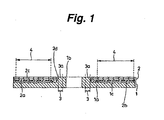
- Fig. 1 is a cross sectional view showing an optical disc according to the first embodiment of the invention.
- Fig. 2 is a cross sectional view showing an injection molding apparatus for molding a disc-shaped substrate according to the first embodiment of the invention.
- Fig. 3 is a cross sectional view showing a replica substrate which is molded by the injection molding apparatus for molding the disc-shaped substrate according to the first embodiment of the invention.
- Fig. 4 is a cross sectional view showing a sheet which is used when a light transmitting layer of the optical disc according to the first embodiment of the invention is formed.
- Fig. 5 is a schematic diagram showing an adhering apparatus which is used to adhere the disc substrate and the sheet according to the first embodiment of the invention.
- Fig. 1 is a cross sectional view showing an optical disc according to the first embodiment of the invention.
- Fig. 2 is a cross sectional view showing an injection molding apparatus for molding a disc-shaped substrate according to the first embodiment of the invention.
- Fig. 3 is a cross sectional
- FIG. 6 is a cross sectional view showing chucking means for clamping the optical disc according to the first embodiment of the invention is formed.
- Fig. 7 is a cross sectional view showing an optical disc according to the second embodiment of the invention.
- Fig. 8 is a cross sectional view showing an injection molding apparatus for molding a disc-shaped substrate according to the second embodiment of the invention.
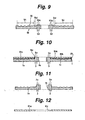
- Fig. 9 is a cross sectional view showing a replica substrate which is molded by the injection molding apparatus for molding the disc-shaped substrate according to the second embodiment of the invention.
- Fig. 10 is a cross sectional view showing an optical disc according to the third embodiment of the invention.
- Fig. 11 is a cross sectional view showing a replica substrate according to the third embodiment of the invention.
- Fig. 11 is a cross sectional view showing a replica substrate according to the third embodiment of the invention.
- FIG. 12 is a cross sectional view showing a light transmitting sheet according to the third embodiment of the invention.
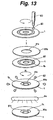
- Fig. 13 is a schematic diagram showing a forming method of a light transmitting layer according to the third embodiment of the invention.
- Fig. 14 is a cross sectional view showing an injection molding apparatus for molding a disc-shaped substrate according to the fourth embodiment of the invention.
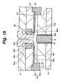
- Fig. 15 is a cross sectional view showing an injection molding apparatus for molding a disc-shaped substrate according to the fifth embodiment of the invention.
- Fig. 16 is a cross sectional view showing a conventional injection molding apparatus for molding a disc-shaped substrate.
- Fig. 17 is a cross sectional view showing a replica substrate which is molded by the conventional injection molding apparatus for molding the disc-shaped substrate.
- Fig. 18 is a cross sectional view showing an optical disc in which a clamp reference surface has been set to the surface of the light transmitting layer.
- Fig. 1 shows the optical disc according to the first embodiment.
- a disc substrate 1 is constructed in a manner such that a center hole 1b is formed in a center portion of a disc-shaped replica substrate 1a and an information signal portion 1c is provided on one principal plane on which concave and convex portions have been formed.
- a light transmitting layer 2 is formed on the disc substrate 1.
- a clamping area 3 is set around the center hole 1b.
- the periphery of the center hole 1b of the replica substrate 1a is constructed so that its thickness is larger than that of an information recording area 4 in which the light transmitting layer 2 has been formed.
- the replica substrate 1a has what is called a convex shape such that its center portion is thick and its peripheral portion is relatively thin.
- a clamp reference surface 3a which is used in case of setting the optical disc to a spindle of a recording and reproducing apparatus (they are not shown) has been set to a principal plane on the side of the information signal portion 1c in the clamping area 3 which has been set in a ring shape.
- a substrate thickness of the replica substrate 1a in the clamping area 3 in the periphery of the center hole 1b is selected to a value within a range of, for example, 1.1 to 1.3 mm. In the first embodiment, it is selected to, for example, 1.2 mm.
- a diameter of the innermost rim of the clamping area 3 is selected from a range of 22 to 24 mm. In the first embodiment, it is selected to, for example, 23 mm.
- a diameter of the outermost rim of the ring-shaped clamping area 3 is selected from a range of 32 to 34 mm. In the first embodiment, it is selected to, for example, 33 mm.
- the light transmitting layer 2 is constructed in a manner such that a light transmitting sheet 2a is adhered via an adhesive layer 2b onto one principal plane of the disc substrate 1 on the side where the information signal portion 1c has been provided and a hard coating layer 2c is provided on the surface of the light transmitting sheet 2a on the side opposite to the side where the adhesive layer 2b has been provided.
- Each of the layers constructing the light transmitting layer 2 is made of a material which can transmit at least a laser beam which is used for recording and reproduction.
- a through-hole 2d is formed in a center portion of the light transmitting layer 2.
- a diameter of the through-hole 2d is set to be larger than the outermost rim diameter of the clamping area 3. Specifically speaking, it is set to, for example, 34 mm or more.
- the optical disc constructed as mentioned above is an optical disc of a type such that an information signal is recorded and/or reproduced by irradiating a laser beam onto the disc substrate 1 from the side where the information signal portion 1c exists toward the information signal portion 1c in a predetermined portion in the information recording area 4.
- the foregoing optical disc is constructed in a manner such that the substrate thickness in the clamping area 3 of the disc substrate 1 is almost equal to the total of the substrate thickness of the disc substrate 1 in the information recording area 4 and the film thickness of the light transmitting layer 2.
- the optical disc is constructed in a manner such that a height of clamp reference surface 3a is almost equal to that of the surface of the light transmitting layer 2 from the surface of the disc substrate 1 on the side opposite to the side where the information signal portion 1c has been provided.
- FIG. 2 shows the injection molding apparatus for molding the disc-shaped substrate.
- Fig. 3 shows the replica substrate 1a.
- the injection molding apparatus for molding the disc-shaped substrate according to the first embodiment is constructed so as to have a die 15 in which a fixed die 12 fixed to a stationary platen 11 and a movable die 14 fixed to a stationary platen 13 are arranged so as to face each other.
- a cavity 16 for molding is formed in a gap between the fixed die 12 and the movable die 14.
- the molding cavity 16 constructs, for example, a disc shape and a shape corresponding to the replica substrate 1a which is molded and shown in Fig. 3 is constructed. Details regarding the replica substrate 1a which is molded will be explained hereinlater.
- a through-hole 12a is formed perpendicularly to a lower surface of the fixed die 12 at a center position of a surface portion of the fixed die 12 on the side where the molding cavity 16 is constructed, that is, a center position of the lower surface portion of the fixed die 12.
- a sprue bush supporting ring 12b having a cylindrical shape pierces the through-hole 12a and is provided therein.
- the sprue bush supporting ring 12b of the fixed die 12 has a shape such that a front edge side which faces the molding cavity 16 is inserted into the fixed die 12 side.
- a sprue bush 12c is fitted to the sprue bush supporting ring 12b.
- the sprue bush 12c fitted to the sprue bush supporting ring 12b has a columnar shape.
- the sprue bush 12c has a resin injection hole 12d formed along a center axis of the columnar shape.
- the resin injection hole 12d is used to inject a synthetic resin material such as a fused polycarbonate resin or the like which is supplied from an injecting apparatus (not shown) into the molding cavity 16 so as to flow therein.
- the sprue bush 12c has a shape such that its front edge portion is inserted from the molding cavity 16 to the fixed die 12 side.
- the front edge portion of the sprue bush 12c in which an opening edge of the resin injection hole 12d has been formed faces the molding cavity 16.
- the sprue bush supporting ring 12b is constructed in a manner such that one end portion of this ring on the side where it faces the molding cavity 16 has a ring convex shape comprising a portion which constructs the same surface as a stamper, which will be explained hereinlater, and a portion which constructs the same surface as a lower surface of the sprue bush 12c and the other end portion has a flange-shaped collar portion.
- An inner peripheral side of one end portion of the sprue bush supporting ring 12b and an outer peripheral side of one end portion of the sprue bush 12c construct a lower surface portion of the fixed die 12.
- the inner peripheral side of the one end portion of the sprue bush supporting ring 12b and the outer peripheral side of the one end portion of the sprue bush 12c construct an inner surface portion of the molding cavity 16 and become a surface portion of the replica substrate 1a shown in Fig. 3 for molding the clamp reference surface 3a.
- a stamper 17 is attached to the lower surface portion of the fixed die 12, that is, the surface portion of the fixed die 12 on the side where it faces the movable die 14.
- the stamper 17 is used to form, for example, a concave and convex pattern corresponding to the information signal, pregrooves constructing recording tracks, or the like onto the replica substrate 1a.
- the stamper 17 is made of, for example, nickel (Ni) or the like.
- the stamper 17 is formed in a plane ring shape having a center hole 17a in a center portion. A mirror portion constructed so as to have a flat surface is provided in a portion of the center hole 17a which faces the peripheral movable die 14.
- a diameter of the center hole 17a (bore of the stamper 17) is set to be larger than the outermost rim diameter of the clamping area 3 of the replica substrate 1a in order to mold the clamp reference surface 3a of the replica substrate 1a shown in Fig. 3 by the inner peripheral portion of the lower surface of the sprue bush supporting ring 12b and the outer peripheral portion of the lower surface of the sprue bush 12c.
- the cavity 16 for molding which is constructed when the fixed die 12 and movable die 14 are arranged so as to face each other is constructed in a manner such that an interval between the inner peripheral side of the lower edge surface of the sprue bush supporting ring 12b and the lower edge outer peripheral side of the sprue bush 12c and the upper surface 14b of the movable die 14 in a portion of the replica substrate 1a shown in Fig. 3 where the clamp reference surface 3a is located is larger than an interval between the lower surface of the stamper 17 and an upper surface 14b of the movable die 14 in a portion of the replica substrate 1a shown in Fig. 3 where the information recording area 4 is located.
- the stamper 17 is positioned by fitting the center hole 17a formed in the center portion to the outside of the front edge portion of the sprue bush supporting ring 12b. That is, the diameter of the center hole 17a (bore of the stamper 17) corresponds to an outer diameter of the ring convex shape in the front edge portion of the sprue bush supporting ring 12b.
- the stamper 17 is supported by a stamper outer peripheral holder 18 attached to the fixed die 12 in a manner such that its outer peripheral edge side is sandwiched between the fixed die 12 and the holder 18.
- the stamper outer peripheral holder 18 is formed in a ring shape and attached to the outer peripheral side portion on the lower surface side of the fixed die 12, thereby constructing the outer peripheral edge portion of the molding cavity 16.
- a stamper sucking mechanism serving as stamper sucking means is provided for the fixed die 12.
- the stamper sucking mechanism is constructed in a manner such that air existing between the fixed die 12 and the stamper 17 is exhausted to the outside by a vacuum pump (not shown) via suction holes 19 formed on the periphery of the front edge portion of the sprue bush supporting ring 12b at a lower surface 12e of the fixed die 12.
- the suction holes 19 are located outside of the outermost rim of the clamping area 3 in the replica substrate 1a which is molded by using the injection molding apparatus for molding the disc-shaped substrate, that is, they are located on the outer peripheral side of the center hole 17a of the stamper 17.
- a plurality of suction holes 19 are arranged in a circumferential shape and formed.
- a radius of the circumferential shape on which the suction holes 19 are arranged and formed is equal to, for example, 34.3 mm.
- 20 suction holes 19 are arranged and formed along this circumference.
- An opening diameter of each suction hole 19 is equal to, for example, 0.2 mm.
- suction holes 19 it is also possible to form ring-shaped gap portions between the front edge portion of the sprue bush supporting ring 12b and the lower surface 12e of the fixed die 12 and use suction slits arranged in those gap portions.
- the suction holes 19 are communicated with a gas emission path 20 provided between an outside surface of the sprue bush supporting ring 12b and an inner wall surface of the through-hole 12a of the fixed die 12.
- the gas emission path 20 is communicated with the outside via a tunnel portion 21 formed in the fixed die 12.
- the tunnel portion 21 is formed from the center side of the fixed die 12 toward the outside surface in the radial direction of the molding cavity 16.
- An upper edge side of the gas emission path 20, that is, a gap portion 22 between a rear edge portion of the sprue bush supporting ring 12b and the upper surface portion of the fixed die 12 is closed by the stationary platen 11 via an O-ring (not shown).
- a vacuum hose 23 is attached to the outside surface portion of the fixed die 12 so as to be communicated with the tunnel portion 21.
- the vacuum hose 23 is connected to a vacuum pump (not shown) via a valve apparatus 24. That is, when the valve apparatus 24 is opened, the vacuum pump sucks air existing between the lower surface 12e of the fixed die 12 and the stamper 17 and exhausts it to the outside via the vacuum hose 23, tunnel portion 21, gas emission path 20, and suction holes 19.
- a suction pressure is set to, for example, 1.4 ⁇ 10 3 Pa (1/72 atm).
- a through-hole 14a is formed at a center position of the movable die 14 so as to be perpendicular to the upper surface portion of the movable die 14. That is, the through-hole 14a is formed at a position which faces the front edge surface of the sprue bush 12c supported by the fixed die 12.
- a sleeve 25 having a cylindrical shape pierces the through-hole 14a formed in the movable die 14 and is arranged in the through-hole 14a. Further, a columnar punch 26 is inserted and arranged into the sleeve 25. The punch 26 can be moved forward and backward to/from the sleeve 25 and is supported by the sleeve 25.
- the sleeve 25 is supported by the movable die 14 so as to be movable forward and backward to/from the movable die 14.
- a front edge surface of the sleeve 25 which faces the molding cavity 16 is inserted into the movable die 14 slightly downwardly from the upper surface portion of the movable die 14.
- a front edge surface of the punch 26 which faces the molding cavity 16 is projected slightly upwardly from the front edge surface of the sleeve 25.
- a stamper 17 whose thickness is equal to or larger than 0.45 mm, preferably, 0.5 mm or more and whose bore is larger than the outermost rim diameter of the clamping area 3 is used.
- the stamper 17 whose thickness is equal to, for example, 0.5 mm, whose bore is equal to, for example, 22 mm, and which is made of, for example, Ni is used.
- the molding cavity 16 is formed by arranging the movable die 14 so as to face the fixed die 12.
- a fused synthetic resin material such as PC or the like is injected into the molding cavity 16 from the foregoing injecting apparatus (not shown) via the resin injection hole 12d of the sprue bush 12c so as to be filled in the cavity 16.
- the synthetic resin material in the fused state flows from the center portion toward the outer peripheral side.
- closing to compress the synthetic resin material filled in the molding cavity 16 is executed.
- the synthetic resin material is solidified by cooling.
- the replica substrate 1a corresponding to the molding cavity 16 is formed.
- the clamp reference surface 3a on one principal plane side of the clamping area 3 of the replica substrate 1a is molded by the outer peripheral side of the lower surface portion of the sprue bush supporting ring 12b and the inner peripheral side of the lower surface portion of the sprue bush 12c.
- the center hole 1b of the replica substrate 1a is formed by projecting the punch 26 to the fixed die 12 side. After that, opening for removing the movable die 14 so as to be away from the fixed die 12 is executed while the sleeve 25 is projected to the fixed die 12 side. Thus, the molded replica substrate 1a is away from the die 15. By removing the replica substrate 1a so as to be away from the fixed die 12, the molding of the disc-shaped substrate is completed.
- the replica substrate 1a molded as mentioned above is constructed in a manner such that a thickness of a peripheral portion of the center hole 1b is larger than that in the information recording area 4.
- the clamp reference surface 3a serving as a reference surface at the time when the optical disc is put to the spindle of the recording and reproducing apparatus (they are not shown in Fig. 3) is set into the inner peripheral portion of a recording surface 5 on the inside of the information recording area 4.
- the innermost rim diameter of the clamping area 3 which is set by the clamp reference surface 3a is equal to, for example, 23 mm and the outermost rim diameter is equal to, for example, 33 mm.
- the information recording area 4 to which the concave and convex portions which form a mirror image in correspondence to the stamper 17 have been transferred is formed on the recording surface 5 of the replica substrate 1a and a mirror surface 6 is formed on the side opposite to the recording surface 5.
- the information signal portion 1c is formed onto the recording surface 5 of the replica substrate 1a shown in Fig. 3 on which the concave and convex portions have been formed.
- the information signal portion 1c is constructed by forming a reflective film, a film made of a magnetooptic material, a film made of a phase change material, an organic pigment film, or the like onto the concave/convex recording surface 5 in the information recording area 4.
- a reflective film for example, Al or the like is used as a material of the reflective film.
- the information signal portion 1c is constructed by a single-layer film or a laminate film having at least the reflective film made of, for example, Al or the like.
- the information signal portion 1c is constructed by a single-layer film or a laminate film having at least a film made of a magnetooptic material or a film made of a phase change material.
- the information signal portion 1c is constructed by a single-layer film or a laminate film having at least a film made of an organic pigment material or a film made of a write-once type phase change material.
- the replica substrate 1a comprises a disc-shaped PC substrate such that, for example, a thickness of at least the clamping area 3 is equal to 1.2 mm and a thickness of the information recording area 4 is equal to 1.1 mm.
- a diameter (outer diameter) of the replica substrate 1a is equal to, for example, 120 mm and an opening diameter (bore) of the center hole 1b is equal to, for example, 15 mm.
- the information signal portion 1c on one principal plane of the replica substrate 1a is a laminate film obtained by sequentially laminating a first dielectric layer having a film thickness of 18 nm and comprising a mixture (ZnS - SiO 2 ) of zinc sulfide (ZnS) and silicon oxide (SiO 2 ), a phase change recording layer having a film thickness of 24 nm and comprising a GeSbTe alloy layer, and a second dielectric layer having a film thickness of 100 nm and comprising ZnS - SiO 2 onto a reflective layer having a film thickness of 100 nm and comprising an Al alloy.
- a first dielectric layer having a film thickness of 18 nm and comprising a mixture (ZnS - SiO 2 ) of zinc sulfide (ZnS) and silicon oxide (SiO 2 )
- a phase change recording layer having a film thickness of 24 nm and comprising a GeSbTe alloy layer
- the light transmitting layer 2 is formed onto the disc substrate 1 on which the information signal portion 1c has been formed.
- a sheet which is used to form the light transmitting layer 2 according to the first embodiment will be described.
- a sheet 7 according to the first embodiment is shown in Fig. 4.
- the sheet 7 which is used to manufacture the optical disc according to the first embodiment has a structure such that it is punched and formed in a plane ring shape and the through-hole 2d is formed at a center in a manner similar to the replica substrate 1a.
- Dimensions of the light transmitting sheet 2a are set in a manner such that a diameter (outer diameter) of the light transmitting sheet 2a is set to be smaller than the outer diameter of the replica substrate 1a and set to, for example, 119 mm, and a diameter (bore) of the through-hole 2d is set to be larger than the outermost rim diameter (for example, 33 mm diameter) of at least the clamping area 3 and set to, for example, 34 mm.
- the light transmitting sheet 2a is made of, for example, a thermoplastic resin which is used at least for recording and reproduction of the optical disc and has light transmitting performance for the laser beam.
- the thermoplastic resin is, for example, polycarbonate (PC) or a methacrylic resin such as polymethyl methacrylate (polymethacrylic methyl) or the like. It is preferable that the light transmitting sheet is made of the same kind of material as that of the replica substrate 1a.
- a thickness of the light transmitting sheet 2a is equal to, for example, 70 ⁇ m. The thickness of the light transmitting sheet 2a is determined in consideration of the film thickness of the light transmitting layer 2.
- FIG. 5 shows such a laminating apparatus.
- a laminating apparatus 30 is constructed by attaching a fixed stage 31 and a movable stage 32 to positions which face each other.
- the fixed stage 31 is used to mount the sheet 7 serving as a light transmitting layer 2 and constructed so that the sheet 7 can be put thereon. That is, a vertical motion pin 33 which is movable in such a direction as to be projected and inserted from/into the fixed stage 31 is provided in a portion of the fixed stage 31 which faces the movable stage 32. A diameter of the vertical motion pin 33 is equal to the diameter of the through-hole 2d of the sheet 7 mentioned above. By fitting the through-hole 2d of the sheet 7 to the vertical motion pin 33, the sheet 7 can be put onto the fixed stage 31.
- a substrate positioning pin 34 which projects in a columnar shape is attached onto the vertical motion pin 33.
- a diameter of the substrate positioning pin 34 is almost equal to the diameter of the center hole 1b of the disc substrate 1 mentioned above.
- the substrate positioning pin 34 can support the disc substrate 1 by the vertical motion pin 33 while aligning the center of the disc substrate 1.
- the sheet 7 can be put by fitting to the vertical motion pin 33 and the disc substrate 1 can be supported by the vertical motion pin 33 by fitting the disc substrate 1 to the substrate positioning pin 34.
- a pad 35 made of, for example, an elastic member such as rubber or the like is attached onto the surface of a portion of the movable stage 32 which faces the fixed stage 31.
- the pad 35 has, for example, a partial spherical shape comprising one of the portions obtained by dividing a sphere by a predetermined plane or a conical shape.
- a cross sectional portion or a plane portion is fixed to a principal plane of the movable stage 32 which faces the fixed stage 31. Rubber hardness of the pad 35 is equal to, for example, 60.
- the laminating apparatus 30 according to the first embodiment is constructed as mentioned above.
- the disc substrate 1 and sheet 7 are laminated by using the laminating apparatus 30 constructed as mentioned above. That is, first, the sheet 7 is put onto the fixed stage 31 in a manner such that the through-hole 2d is fitted to the vertical motion pin 33. At this time, the sheet 7 is put in a manner such that the adhesive layer 2b side of one of the surfaces of the sheet faces the movable stage 32. After that, the disc substrate 1 is put so as to be supported by the vertical motion pin 33 while it is fitted to the substrate positioning pin 34. At this time, the disc substrate 1 is supported by the vertical motion pin 33 and put in a manner such that the principal plane on which the information signal portion 1c has been provided, that is, the recording surface on which the clamp reference surface 3a has been set faces the adhesive layer 2b.
- the movable stage 32 is moved toward the fixed stage 31 (downwardly in Fig. 5).
- the substrate positioning pin 34 is pressed by the pad 35.
- the vertical motion pin 33 is inserted into the fixed stage 31 through the disc substrate 1.
- the principal plane of the disc substrate 1 on which the information signal portion 1c has been provided and the adhesive layer 2b of the sheet 7 are adhered with pressure.
- the movable stage 32 is released in such a direction as to be away from the fixed stage 31. After that, the disc substrate 1 and sheet 7 which were adhered are removed from the fixed stage 31.
- the light transmitting layer 2 is formed onto the disc substrate 1 and the desired optical disc shown in Fig. 1 is manufactured.
- FIG. 6 shows a chucking portion according to the first embodiment.
- a disc mounting table 42, a center positioning pin 43, and a magnetic metal plate 44 are sequentially coupled and provided in an upper portion of a rotary shaft 41.
- the rotary shaft 41 is coupled with a motor (not shown) and can be rotated around a center in a cross sectional plane that is perpendicular to the longitudinal direction of the rotary shaft 41.
- the disc mounting table 42 is used to mount the optical disc.
- the optical disc is put onto the disc mounting table 42 while coming into contact with the principal plane of the disc substrate 1 in the clamping area 3, that is, the clamp reference surface 3a.
- the upper surface of the disc mounting table 42 onto which the optical disc is put has a ring shape, its innermost rim diameter is equal to, for example, 26 mm, and its outermost rim diameter is equal to, for example, 32 mm.
- a permanent magnet (not shown) has been inserted in the disc mounting table 42 and, specifically speaking, the permanent magnet is coated with a resin such as polyimide or the like.
- the center positioning pin 43 is used to position the center of the optical disc.
- the center positioning pin 43 is constructed so that it can be inserted into a center hole of the optical disc (center hole 1b of the disc substrate 1) and its center coincides almost with an auto-rotational center of the rotary shaft 41.
- the magnetic metal plate 44 is made of a magnetic material and used to clamp the optical disc put on the disc mounting table 42 from the mirror surface 6 side of the disc substrate 1.
- a cross sectional surface of the magnetic metal plate 44 which is parallel with the mounting surface of the disc mounting table 42 has a ring shape.
- An innermost rim diameter of the ring shape is equal to, for example, 26 mm and an outermost rim diameter is equal to, for example, 32 mm.
- the chucking portion 40 is constructed in a manner such that in the clamping area 3, the optical disc is clamped by the disc mounting table 42 which is in contact with the clamp reference surface 3a and the magnetic metal plate 44 which is in contact with the mirror surface 6 side and this optical disc can be clamped.
- a force which is applied when the optical disc is clamped by the disc mounting table 42 and magnetic metal plate 44, that is, a clamping force is equal to, for example, 2N in case of the consumer use and to, for example, 10N in case of the industrial use.
- the optical disc is clamped by the chucking portion 40 constructed as mentioned above.
- the recording and reproduction to/from the information signal portion 1c are executed by a method whereby a laser beam L1 which has been emitted from a semiconductor laser (not shown) and passed through a lens in 2 groups is irradiated to the information signal portion 1c from the light transmitting layer 2 side of the optical disc.
- a semiconductor laser serving as a light source of the laser beam it is possible to mention a GaN system semiconductor laser (a band of a light emitting wavelength of 400 nm; blue light emission), a ZnSe system semiconductor laser (a band of a light emitting wavelength of 500 nm; green), an AlGaInP system semiconductor laser (light emitting wavelength of about 635 to 680 nm; red), or the like.
- a GaN system semiconductor laser a band of a light emitting wavelength of 400 nm; blue light emission
- a ZnSe system semiconductor laser a band of a light emitting wavelength of 500 nm; green
- an AlGaInP system semiconductor laser light emitting wavelength of about 635 to 680 nm; red
- the replica substrate 1a in which the thickness of the periphery of the center hole 1b is larger than that in the information recording area 4 is injection-molded by the injection molding apparatus for molding the disc-shaped substrate, and the clamp reference surface 3a is set to the recording surface 5 side in the portion of the disc substrate 1 in which the thickness of the periphery of the center hole 1b is large, so that the clamp reference surface 3a can be made of the substrate material. Therefore, even in case of clamping and rotating the optical disc in which the lubricating performance of the surface of the light transmitting layer 2 has been improved, the race of the optical disc can be prevented, and rigidity of the disc substrate 1, that is, the optical disc can be improved.
- the substrate thickness of the periphery of the center hole 1b of the replica substrate 1a is set to be larger than the conventional substrate thickness, that is, the substrate thickness in the information recording area 4, a large C plane can be assured on the recording surface 5 side near the center hole 1b. Therefore, burrs which are caused when the center hole 1b of the disc substrate 1 is formed by the punch 26 of the injection molding apparatus for molding the disc-shaped substrate can be easily removed.
- the clamp reference surface 3a which has been flattened at high precision and has high flatness can be formed. Eccentricity upon rotation of the optical disc can be suppressed.
- the thin light transmitting layer 2 is provided on the principal plane side of the replica substrate 1a and, also in the case where the optical disc to/from which the information signal is recorded and/or reproduced by irradiating the laser beam from the light transmitting layer 2 side is put to the spindle of the recording and reproducing apparatus or the reproducing apparatus, the optical disc can be rotated at high precision. In the optical disc, therefore, precision and reliability at which the recording and/or reproduction can be sufficiently performed can be assured, and its recording characteristics and reproducing characteristics can be improved.
- FIG. 7 shows the optical disc according to the second embodiment.
- a disc substrate 51 is constructed in a manner such that a center hole 51b is formed in a center portion of a disc-shaped replica substrate 51a and an information signal portion 51c is provided on one principal plane on which concave and convex portions have been formed.
- a light transmitting layer 52 is formed on the principal plane of the disc substrate 51.
- the periphery of the center hole 51b of the replica substrate 51a is constructed so that its thickness is larger than that of an information recording area 4 in which the light transmitting layer 52 has been formed.
- the replica substrate 51a has what is called a convex shape such that its center portion is thick and its peripheral portion is relatively thin.
- a clamping area 53 is set in a ring shape.
- a clamp reference surface 3a which is used in case of putting the optical disc to the spindle of the recording and reproducing apparatus (they are not shown) has been set to a principal plane on the side of the information signal portion 51c in the clamping area 53.
- An innermost rim diameter of the ring-shaped clamping area 53 is selected from a range of 22 to 24 mm. In the second embodiment, it is selected to, for example, 23mm. An outermost rim diameter of the clamping area 53 is selected from a range of 32 to 34 mm. In the second embodiment, it is selected to, for example, 33 mm.
- a stamper pressing groove 51d formed upon injection molding is formed on the surface of the replica substrate 51a where the clamp reference surface 53a has been set, that is, in a portion on the outer side from the outermost rim of the clamping area 53, namely, a portion on the inner side from the innermost rim of an information recording area 54 where the information signal is recorded.
- the light transmitting layer 52 is constructed in amanner such that a light transmitting sheet 52a is adhered via an adhesive layer 52b onto one principal plane of the disc substrate 51 on the side where the information signal portion 51c has been provided.
- a through-hole 52c is formed in a center portion of the light transmitting layer 52.
- a diameter of the through-hole 52c is set to be larger than the outermost rim diameter of the clamping area 53. Specifically speaking, it is set to, for example, 34 mm or more.
- the optical disc constructed as mentioned above is an optical disc of a type such that the information signal is recorded and/or reproduced by irradiating the laser beam onto the disc substrate 51 from the side where the information signal portion 51c exists toward the information signal portion 51c in a predetermined portion in the information recording area 54.
- the foregoing optical disc is constructed in a manner such that the substrate thickness in the clamping area 3 of the disc substrate 1 is almost equal to the total of the substrate thickness of the disc substrate 1 in the information recording area 4 and the film thickness of the light transmitting layer 2.
- the optical disc is constructed in a manner such that the height of the clamp reference surface 3a is almost equal to that of the surface of the light transmitting layer 2 from the surface of the disc substrate 1 on the side opposite to the side where the information signal portion 1c has been provided.
- FIG. 8 shows the injection molding apparatus for molding the disc-shaped substrate according to the second embodiment.
- the disc-shaped substrate molding injection molding apparatus for molding the disc substrate is constructed so as to have a die 65 in which a fixed die 62 fixed to a stationary platen 61 and a movable die 64 fixed to a stationary platen 63 are arranged so as to face each other.
- a cavity 66 for molding is formed in a gap between the fixed die 62 and the movable die 64.
- the molding cavity 66 has a shape corresponding to the replica substrate 51a which is molded and shown in Fig. 9.
- a through-hole 62a is formed at a center position of the fixed die 62 in the injection molding apparatus for molding the disc-shaped substrate shown in Fig. 8.
- a sprue bush supporting ring 62b having almost a ring shape pierces the through-hole 62a and is provided therein.
- the sprue bush supporting ring 62b of the fixed die 62 has a shape such that a front edge side which faces the molding cavity 66 is inserted into the fixed die 62 side. That is, a shape of the molding cavity 66 which is formed when the fixed die 62 and movable die 64 are arranged so as to face each other is constructed in a manner such that an interval between a lower surface 62e of the fixed die 62 and an upper surface of the movable die 64 in a portion of the replica substrate 51a where the clamp reference surface 53a is located is larger than an interval between the lower surface 62e of the fixed die 62 and an upper surface 64b of the movable die 64 in a portion of the replica substrate 51a shown in Fig.
- a diameter of a front edge side of the sprue bush supporting ring 62b which faces the molding cavity 66 is reduced in a stairway manner.
- a sprue bush 62c is fitted to the sprue bush supporting ring 62b.
- the sprue bush 62c fitted to the sprue bush supporting ring 62b has a cylindrical shape.
- the sprue bush 62c has a resin injection hole 62d formed along a center axis of the cylindrical shape.
- the resin injection hole 62d is used to inject a synthetic resin material such as a fused polycarbonate resin or the like which is supplied from the injecting apparatus (not shown) into the molding cavity 66 so as to flow therein.
- the sprue bush 62c has a shape such that its front edge portion is inserted from the molding cavity 66 to the fixed die 62 side.
- the front edge portion of the sprue bush 62c in which an opening edge of the resin injection hole 62d has been formed faces the molding cavity 66.
- An outer peripheral side of this front edge portion constructs the same surface as the portion where the sprue bush supporting ring 62b has been inserted.
- the sprue bush supporting ring 62b is constructed in a manner such that its lower surface comprises a portion which becomes the same surface as the lower surface of the sprue bush 62c and the other end portion has a flange-shaped collar portion.
- a surface (lower surface) of one end portion of the sprue bush supporting ring 62b constructs a lower surface portion of the fixed die 62.
- the surface (lower surface) of one end portion of the sprue bush supporting ring 62b constructs an inner surface portion of the molding cavity 16 and becomes a surface portion of the replica substrate 51a shown in Fig. 9 where the clamp reference surface 53a is molded.
- a stamper 67 is attached to a surface portion of the die constructing the molding cavity 66 of the fixed die 62, that is, the surface portion of the fixed die 62 on the side where it faces the movable die 64.
- the stamper 67 is used to form, for example, a concave and convex pattern corresponding to the information signal, pregrooves constructing recording tracks, or the like onto the replica substrate 51a.
- the stamper 67 is made of, for example, Ni or the like.
- the stamper 67 is formed in a plane ring shape having a center hole 67a in a center portion and formed in a plane ring shape in which a mirror portion constructed so as to have a flat surface is provided in a portion of the center hole 67a which faces the peripheral movable die 64.
- a diameter of the center hole 67a (bore of the stamper 67) is set to be larger than the outermost rim diameter of the clamping area 53 of the replica substrate 51a in order to mold the clamp reference surface 53a of the replica substrate 51a shown in Fig. 3 by the outer peripheral portion of the lower surface of the sprue bush supporting ring 62b and the outer peripheral portion of the lower surface of the sprue bush 12c.
- the stamper 67 is constructed in a manner such that it can be supported by a cylindrical stamper inner peripheral holder 68 at an inner peripheral edge of the center hole 67a and can be supported by a ring-shaped stamper outer peripheral holder 69 at a disc- shaped outer peripheral edge.
- the stamper 67 is attached to the lower surface 62e of the fixed die 62 by the stamper inner peripheral holder 68 and stamper outer peripheral holder 69.
- the stamper inner peripheral holder 68 for supporting the peripheral edge of the center hole 67a on the inner peripheral edge side of the stamper 67 is fitted to the outer peripheral side of the sprue bush supporting ring 62b, located on the front edge side of the sprue bush 62c, and attached to the fixed die 62.
- a claw portion 68a for supporting the stamper is provided in an outer peripheral portion of the stamper inner peripheral holder 68 on the side of the molding cavity 66.
- the stamper supporting claw portion 68a is used to support a peripheral edge of the center hole 67a.
- a through-hole 64a is formed at a center position of the movable die 64.
- a cylindrical sleeve 70 pierces the through-hole of the movable die 64 and is provided therein.
- the sleeve 70 is constructed so as to be movable forward and backward into/from the molding cavity 66 and is supported by the movable die 64.
- a front edge surface of the sleeve 70 which faces the molding cavity 66 is slightly inserted into the movable die 64.
- a columnar punch 71 is fitted into the cylinder of the sleeve 70.
- a front edge surface of the punch 71 which faces the molding cavity 66 is slightly projected from the front edge surface of the sleeve 70.
- the replica substrate 51a shown in Fig. 9 is formed by this injection molding method.
- a stamper 67 a stamper whose thickness is equal to or larger than 0.45 mm, preferably, 0.5 mm or more and which is made of, for example, Ni is used.
- a recording surface 55 is provided on one principal plane of the replica substrate 51a and a mirror surface 56 is provided on the other surface in a manner similar to the first embodiment.
- the clamping area 53 is set in an inner peripheral portion on the recording surface 55 side.
- the clamp reference surface 53a is set to the recording surface 55 side of the clamping area 53.
- the stamper pressing groove 51d formed by the stamper supporting claw portion 68a upon injection molding is provided on the recording surface 55 of the replica substrate 51a, that is, in the portion on the outer side from the outermost rim of the clamping area 53 and on the inner side from the innermost rim of the information signal portion 51c. Since the other structure of the replica substrate 51a is similar to that of the first embodiment, its description is omitted.
- the information signal portion 51c is formed on the principal plane on which the recording surface 55 of the replica substrate 51a has been formed.
- the light transmitting layer 52 is formed on the information signal portion 51c by using the laminating apparatus shown in Fig. 4.
- the optical disc shown in Fig. 7 is manufactured.
- the stamper pressing groove 51d is formed and left on the outer side of the outermost rim of the clamping area 53 and on the inner side from the innermost rim of the information recording area 54, on the principal plane on the side where the light transmitting layer 52 has been formed.
- the replica substrate 51a of the disc substrate 51 constructing the optical disc has been formed in a convex shape, a high frictional force at the time when the disc is clamped and rotated can be assured on the clamp reference surface 53a, flatness of high precision can be assured, and the surface 53a can have high plane surface performance. Therefore, an effect similar to that in the first embodiment can be obtained.
- Fig. 10 shows the optical disc according to the third embodiment.
- Fig. 11 shows a replica substrate constructing a disc substrate.
- Fig. 12 shows a light transmitting sheet.
- a light transmitting layer 81 comprising a light transmitting sheet 41a and an adhesive layer 81b is formed on the principal plane of the disc substrate 1 on which the information signal portion 1c has been provided.
- the replica substrate 1a according to the third embodiment is similar to that in the first embodiment.
- the sheet which is used in the third embodiment is constructed by the light transmitting sheet 81a.
- the light transmitting sheet 81a has a structure such that it is punched in a plane ring shape and formed, and a through-hole 81c is formed at a center.
- Dimensions of the light transmitting sheet 81a are set in a manner such that a diameter (outer diameter) is set to, for example, 119 mm which is equal to or smaller than the outer diameter (for example, 120 mm) of the replica substrate 1a, and a diameter (bore) of the through-hole 81c is set to be larger than the outermost rim diameter of the clamping area 3, specifically speaking, it is set to, for example, 34 mm.
- the light transmitting sheet 81a is made of, for example, a thermoplastic resin having light transmitting performance which satisfies optical characteristics by which at least ultraviolet rays can be transmitted.
- the thermoplastic resin is, for example, PC or a methacrylic resin such as polymethyl methacrylate (polymethacrylic methyl) or the like.
- the light transmitting sheet is made of the same kind of material as that of the replica substrate 1a.
- a thickness of the light transmitting sheet 81a is equal to, for example, 95 ⁇ m. The thickness of the light transmitting sheet 81a is determined in consideration of a film thickness of the light transmitting layer 81 which is finally formed.
- a manufacturing method of the optical disc according to the third embodiment will now be described.
- the manufacturing method of the disc substrate 1 according to the third embodiment is similar to that in the first embodiment, its explanation is omitted.
- Fig. 13 shows a forming step of the light transmitting layer 81 according to the third embodiment.
- an ultraviolet hardening resin 82 is supplied and coated onto the principal plane of the disc substrate 1 on which the information signal portion 1c has been formed.
- the ultraviolet hardening resin 82 is supplied in, for example, a plane ring shape from a nozzle port of an ultraviolet hardening resin supplying portion 83 toward the inner peripheral side on the principal plane of the disc substrate 1.
- the ultraviolet hardening resin supplying portion 83 for emitting the ultraviolet hardening resin 82 and the disc substrate 1 are relatively rotated.
- an ultraviolet hardening resin 82 for example, a resin whose viscosity is equal to 0.1 Pa ⁇ s (100 cps) is used.
- the center hole 1b of the disc substrate 1 and the through-hole 81c at the center of the light transmitting sheet 81a are positioned.
- the plane ring-shaped light transmitting sheet 81a is put onto the principal plane of the disc substrate 1 to which the ultraviolet hardening resin 82 has been supplied.
- the disc substrate 1 and light transmitting sheet 81a are rotated in an in-plane direction (M direction in C in Fig. 13) around a rotary shaft as a center.
- the ultraviolet hardening resin 82 on the disc substrate 1 is fully supplied to a gap between the disc substrate 1 and the light transmitting sheet 81a.
- the surplus ultraviolet hardening resin 82 is fully taken off.
- a rotational speed of each of the disc substrate 1 and the light transmitting sheet 81a is equal to, for example, 83.3 sec -1 (5000 rpm) and a rotating time is equal to, for example, 20 sec.
- the ultraviolet hardening resin 82 is supplied to the surface of the disc substrate 1 on the side opposite to the side where the light transmitting sheet 81a has been adhered and a protective layer (not shown) made of the ultraviolet hardening resin 82 is formed, even in the ultraviolet hardening resin 82 which forms the protective layer, the surplus ultraviolet hardening resin 82 is fully taken off by the rotation in the in-plane direction and uniformly coated, so that the protective layer (not shown) of a uniform thickness is formed.
- the disc substrate 1 After the ultraviolet hardening resin 82 was fully supplied to the gap between the disc substrate 1 and the light transmitting sheet 81a and the surplus ultraviolet hardening resin 82 was fully taken off, as shown in D in Fig. 13, the disc substrate 1 is disposed into an irradiating range of an ultraviolet light source 84 constructed so that it can emit ultraviolet rays. At this time, the disc substrate 1 is arranged so that the side where the light transmitting sheet 81a has been put faces the side where the ultraviolet light source 84 has been disposed. After that, the ultraviolet rays are irradiated from the ultraviolet light source 84 onto the ultraviolet hardening resin 82 on the principal plane of the disc substrate 1 via the light transmitting sheet 81a.
- An integrating intensity at this time is set to, for example, 500 mJ/cm 2 .
- the ultraviolet hardening resin 82 is hardened between the disc substrate 1 and the light transmitting sheet 81a.
- the light transmitting sheet 81a is adhered onto an upper layer of the information signal portion 1c of the surface on the principal plane of the disc substrate 1 via the adhesive layer 81b made of the hardened ultraviolet hardening resin.
- the desired optical disc in which the information signal portion 1c and the light transmitting layer 81 comprising the adhesive layer 81b and light transmitting sheet 81a have been formed on the principal plane of the replica substrate 1a is manufactured.
- the disc substrate 1 of what is called a convex shape in which the substrate thickness of the periphery of the center hole 1b is larger than that in the information recording area 4 is manufactured, and in the optical disc using this disc substrate 1, the clamp reference surface 3a is set to the side where the information signal portion 1c around the center hole 1b has been provided. Therefore, an effect similar to that in the first embodiment can be obtained.
- FIG. 13 shows the injection molding apparatus for molding the disc-shaped substrate according to the fourth embodiment.
- a concave and convex pattern which is transferred onto the recording surface 5 of the replica substrate 1a according to the first embodiment is formed onto a lower surface 91a of a fixed die 91.
- a die 92 is constructed by the fixed die 91 and movable die 64. Since the concave and convex pattern which is transferred has been formed on the lower surface 91a of the fixed die 91 as mentioned above, the concave and convex pattern can be formed into the portion of the information recording area 54 of the recording surface 55 of the replica substrate 51a without disposing the stamper 67 onto the lower surface 91a of the fixed die 91 as in the second embodiment.
- Stamper supporting means for fixing the stamper, specifically speaking, suction holes 19, gas emission path 20, tunnel portion 21, gap portion 22, vacuum hose 23, and valve apparatus 24 in the first embodiment and the stamper inner peripheral holder 68, stamper supporting claw portion 68a, and the like in the second embodiment are not provided in the injection molding apparatus for molding the disc-shaped substrate according to the fourth embodiment.
- the stamper outer peripheral holder 69 is used only for positioning the fixed die 91 and movable die 64. Since the other construction of the injection molding apparatus for molding the disc-shaped substrate according to the fourth embodiment is similar to that in the second embodiment, its explanation is omitted.
- the stamper supporting claw portion 68a and the like in the second embodiment are not provided, the stamper pressing groove 51d and the like are not formed.
- the portion of the replica substrate 1a shown in Fig. 3 where the clamping area 3 is molded is the portion of the fixed die 91 on the outer peripheral side of the lower surface of the sprue bush 62c and the lower surface portion of the sprue bush supporting ring 62b. Therefore, the clamp reference surface 3a in the replica substrate 51a shown in Fig. 3 can be flattened at high precision and the clamp reference surface 3a having high plane surface performance can be formed.
- the clamp reference surface 3a can be set onto the principal plane on which the information signal portion 1c has been provided around the center hole 1b of the disc substrate 1, when the disc is clamped and rotated, a high frictional force can be assured. Therefore, an effect similar to that in the first embodiment can be obtained.
- FIG. 15 shows the injection molding apparatus for molding the disc-shaped substrate according to the fifth embodiment.
- the stamper 67 is fixed to one surface of a stamper stationary platen 93 in which a diameter of a center hole is smaller and an outer rim diameter is larger than those of the stamper 67.
- the stamper 67 and an inner edge of the stamper stationary platen 93 are fixed by a claw portion 94a for supporting the stamper stationary platen of an inner peripheral side stamper stationary platen holder 94.
- An outer peripheral edge of the stamper stationary platen 93 is fixed by the stamper outer peripheral holder 69.
- the stamper 67 is fixed to one surface of the stamper stationary platen 93 and adhered to the lower surface of the fixed die 62.
- the stamper 67 is fixed to one surface of the stamper stationary platen 93 whose inner peripheral diameter is smaller and whose outer peripheral diameter is larger than those of the stamper 67.
- An inner edge of the stamper stationary platen 93 is fixed by the claw portion 94a for supporting the stamper stationary platen of the inner peripheral side stamper stationary platen holder 94.
- the portion of the stamper stationary platen supporting claw portion 94a constructing the molding cavity 66 becomes the same plane as the flat surface of the stamper 67.
- the numerical values, the disc substrate materials, and the forming method of the light transmitting layer mentioned in the foregoing embodiments have merely been shown as examples. Numerical values, disc substrate materials, and a forming method of the light transmitting layer which are different from them can be also used as necessary.
- a resin having low water absorbance such as cycloolefine polymer (for example, ZEONEX (registered trademark)) or the like except for polycarbonate can be also used.
- the optical disc to which the invention is applied is an optical disc of the type such that the information signal is recorded and reproduced by irradiating the laser beam onto the disc substrate from the side where the light transmitting layer has been formed, there is no need to consider the transmittance of the laser beam. Therefore, for example, in the foregoing first to fifth embodiments, as a replica substrate, for example, it is possible to use a substrate made of a metal such as Al or the like, a glass substrate, or a substrate made of a resin such as polyolefine, polyimide, polyamide, polyphenylene sulfide, polyethylene terephthalate, or the like.
- the suction holes 19 and gas emission path 20 have been arranged between the front edge portion of the sprue bush supporting ring 12b and the lower surface 12e of the fixed die 12.
- the suction holes 19 and gas emission path 20 can be also formed and provided in the portions of the sprue bush supporting ring 12b or the fixed die 12.
- the flattened clamp reference surface has been set onto the principal plane of the substrate where the information signal portion has been provided. Therefore, even in the case where the optical recording medium which is manufactured by using such a substrate and in which the information signal is recorded and/or reproduced by irradiating the laser beam from the side where the information signal portion has been provided is put to the spindle of the recording and reproducing apparatus and/or the reproducing apparatus, the recording and/or reproduction of the information signal can be executed while the apparatus has the high reliability.
- the substrate in which the clamp reference surface can be set onto one principal plane of the substrate where the information signal portion has been provided can be manufactured.
- the substrate in which the clamp reference surface can be constructed by the flat surface which has been flattened at high precision and has high plane surface performance can be manufactured. Even in the case where the optical recording medium which is manufactured by using such a substrate is clamped and rotated, this optical recording medium can be rotated in a state where high frictional force is assured.
Landscapes
- Engineering & Computer Science (AREA)
- Manufacturing & Machinery (AREA)
- Mechanical Engineering (AREA)
- Manufacturing Optical Record Carriers (AREA)
- Optical Record Carriers And Manufacture Thereof (AREA)
- Moulds For Moulding Plastics Or The Like (AREA)
Abstract
In an optical disc in which an information signal
is recorded/reproduced by irradiating a laser beam to a disc
substrate 1 in which an information signal portion 1c has
been provided on one principal plane from the side where
the information signal portion 1c exists, a clamp reference
surface 3a is set to the information signal portion 1c side
of a replica substrate 1a constructing the optical disc.
The clamp reference surface 3a is set to a flat surface and
a thickness of the replica substrate 1a in a clamping area
3 is set to be larger than that of the convex-shaped replica
substrate 1a in an information recording area 4. The replica
substrate 1a in which a periphery of a center hole 1b is
thicker than the information recording area 4 is used.
Description
The invention relates to an optical recording
medium, its manufacturing method, and an injection molding
apparatus. More particularly, the invention is suitable
when it is applied to an optical recording medium onto/from
which an information signal is recorded and reproduced by
irradiating light from the side of a substrate where an
information signal portion has been formed.
In recent years, in the field of information
recording, various studies and development regarding an
optical information recording system have been being made.
According to the optical information recording system, it
has an advantage such that the recording and reproduction
can be performed in a contactless manner and a recording
density which is one or more digits higher than that of a
magnetic recording system can be accomplished. The optical
information recording system also has an advantage such that
it can cope with various memory formats such as read only
type, write once type, rewritable type, and the like.
Therefore, as a system which enables a cheap file of a large
capacity to be realized, its application to fields of a wide
range from the industrial use to the consumer use is
considered.
Among those formats, particularly, as optical
discs corresponding to the memory format of the read only
type, a digital audio disc (DAD), an optical video disc,
and the like have widely been spread.
A construction of the optical disc such as a
digital audio disc or the like as mentioned above will be
described hereinbelow. That is. in the optical disc, a
reflective layer made of a thin metal film such as an aluminum
(Al) film or the' like and a protective film to protect the
reflective layer from moisture (H2O) or oxygen (O2) in the
atmosphere are sequentially formed on one principal plane
of an optical disc substrate made of a transparent substrate
on which concave/convex patterns such as pits, grooves, and
the like showing an information signal have been formed.
In such an optical disc, in case of reproducing the
information signal, first, reproducing light such as a laser
beam or the like is irradiated to the concave/convex patterns
from the disc substrate side. The information signal is
detected by a difference of reflectance between incident
light and return light of the reproducing light.
Ordinarily, the disc substrate constructing such
an optical disc is made of a synthetic resin material and
molded by using a die apparatus for injection molding. A
disc substrate molding injection molding apparatus for
molding the disc substrate will now be described with
reference to the drawings.
That is, as shown in Fig. 16, the injection molding
apparatus for molding the disc substrate is constructed by
having a die 103 in which a fixed die 101 and a movable die
102 which are fixed to a stationary platen 100 are arranged
so as to face each other. When the fixed die 101 and movable
die 102 are set so as to face each other, a cavity 104 for
molding is formed between the fixed die 101 and the movable
die 102. The cavity 104 for molding has a shape corresponding
to a disc substrate 201 which is molded as shown in Fig.
17.
A through-hole is formed at a center position of
the fixed die 101 in the injection molding apparatus shown
in Fig. 16. A stamper holder supporting member 106 having
almost a ring shape pierces the through-hole. A sprue bush
107 is provided so as to be inserted into the stamper holder
supporting member 106.
The sprue bush 107 has the ring shape and a resin
injection hole 108 is formed along a center axis in the ring
shape. The resin injection hole 108 is constructed so that
a synthetic resin material such as a fused polycarbonate
resin or the like which is supplied from an injecting
apparatus (not shown) can flow into the cavity 104 for molding.
That is, a front edge side of the sprue bush 107 is constructed
so as to face the inside of the cavity 104 for molding. A
diameter of a front edge side of the stamper holder supporting
member 106 which faces the cavity 104 for molding is reduced
in a stairway manner.
A stamper 109 is attached to a surface portion
of the fixed die 101 constructing the cavity 104 for molding,
that is, a surface portion of the fixed die 101 which faces
the movable die 102. The stamper 109 is formed in a disc
shape having a center hole 109a in a center portion. The
stamper 109 is used to form the concave/convex patterns
corresponding to the information signal or pregrooves
constructing recording tracks onto the disc substrate. The
stamper 109 is constructed so that it can be supported at
an inner peripheral edge of the center hole 109a by a stamper
inner peripheral holder 110 in a ring shape and can be
supported at a disc-shaped outer peripheral edge by a stamper
outer peripheral holder 111 in a ring shape, so that the
stamper 109 is attached to the fixed die 101. That is, the
stamper inner peripheral holder 110 which supports the
peripheral edge of the center hole 109a serving as an inner
peripheral edge side of the stamper 109 is fitted to the
outer peripheral side of the stamper holder supporting member
106, located on the front edge side of the sprue bush 107,
and attached to the fixed die 101. A claw portion 110a for
supporting the stamper is provided in an outer peripheral
portion on the molding cavity 104 side of the stamper inner
peripheral holder 110. The claw portion 110a for supporting
the stamper is used to support the peripheral edge of the
center hole 109a of the stamper 109.
On the other hand, a through-hole is formed at
a center position of the movable die 102. A sleeve 112 in
a cylindrical shape penetrates the through-hole of the
movable die 102. The sleeve 112 is constructed so as to
be movable forward and backward into/from the molding cavity
104 and is supported by the movable die. A front edge surface
of the sleeve 112 which faces the molding cavity 104 is
slightly inserted into the movable die 102. A columnar punch
113 is fitted into the cylinder of the sleeve 112. A front
edge surface of the punch 113 which faces the molding cavity
104 is slightly projected from the front edge surface of
the sleeve 112.
A method of forming the disc substrate 201 shown
in Fig. 17 by using the disc substrate molding die apparatus
constructed as mentioned above will now be described.
That is, first, the molding cavity 104 is formed
by confronting the movable die 102 with the fixed die 101.
A fused synthetic resin material such as PC or the like is
injected and filled into the molding cavity 104 from the
foregoing injecting apparatus (not shown) via the resin
injection hole 108 of the sprue bush 107. At this time,
in the molding cavity 104, the synthetic resin material in
the fused state flows from the center portion toward the
outer peripheral side. By moving the movable die 102 toward
the fixed die 101 side, closing to compress the synthetic
resin material filled in the molding cavity 104 is performed.
After that, the synthetic resin material is solidified by
cooling it. Thus, the disc substrate 201 corresponding to
the molding cavity 104 is formed.
A center hole 202 in the disc substrate 201 is
formed by projecting the punch 113 toward the fixed die 101
side. After that, opening to remove the movable die 102
so as to be away from the fixed die 101 is executed while
the sleeve 112 is projected toward the fixed die 101 side.
Thus, the molded disc substrate 201 is away from the die
103. By removing the disc substrate 201 from the fixed die,
the molding of the disc substrate 201 shown in Fig. 17 is
completed.
The center hole 202 formed at the center by the
punch 113 and a stamper pressing groove 203 formed by the
claw portion 110a for supporting the stamper are formed in
the disc substrate 201 molded as mentioned above. Concave
and convex portions serving as a mirror image corresponding
to the stamper 109 are transferred onto one principal plane
of the disc substrate 201, so that an information recording
area 204a is formed. A recording surface 204 including the
information recording area 204a and a mirror surface 205
on the side opposite to the recording surface 204 are formed.
A clamp reference surface 206a serving as a surface which
is clamped when the disc is set to a spindle of a recording
and reproducing apparatus (not shown) is formed in an inner
peripheral portion of the mirror surface 205. The clamp
reference surface 206a is formed by a mirror surface portion
of the movable die 102 upon injection molding.
The disc substrate 201 is manufactured as
mentioned above. An optical disc such as rewritable type
optical disc, read only type optical disc, or the like is
manufactured by using the disc substrate 201.
In the optical disc manufactured by using the disc
substrate 201 as mentioned above, a further high recording
density has been required in recent years. In order to meet
such a requirement for the high recording density, therefore,
a technique for reducing a spot diameter of the reproducing
light by increasing a numerical aperture (NA) of an objective
lens which is used when the reproducing light of an optical
pickup is irradiated has been proposed. Specifically
speaking, although an NA of an objective lens which is used
upon reproduction of a conventional digital audio disc is
equal to 0.45, an NA of an objective lens which is used upon
reproduction of an optical video disc such as a DVD (Digital
Versatile Disc) or the like having a recording capacity which
is 6 to 8 times as large as that of the digital audio disc
is equal to about 0.60. By increasing the numerical aperture
NA as mentioned above, miniaturization of the spot diameter
can be realized.
By accomplishing the large NA of the objective
lens as mentioned above, it is necessary to thin the substrate
in the optical recording medium in order to transmit the
irradiated reproducing light. This is because a permission
amount of an angle (tilt angle) at which a direction
perpendicular to the disc surface is deviated from an optical
axis of the optical pickup is small. This is also because
the tilt angle is easily influenced by aberration or
birefringence due to a thickness of the disc substrate.
Therefore, the tilt angle is set to be as small as possible
by thinning the disc substrate. For example, in the
foregoing digital audio disc, the substrate thickness is
set to about 1.2 mm. In the optical video disc such as a
DVD or the like having the recording capacity which is 6
to 8 times as large as that of the digital audio disc, the
substrate thickness is set to about 0.6 mm.
A further thin substrate is necessary in
consideration of a requirement of realization of a further
high recording density in the future. Therefore, there has
been proposed an optical recording medium constructed in
a manner such that an information signal portion is formed
by forming concave/convex portions onto one principal plane
of the substrate, a reflective film and a light transmitting
layer as a thin film for transmitting the light are
sequentially laminated onto the information signal portion,
and the reproducing light is irradiated from the light
transmitting layer side, thereby reproducing the
information signal. In the optical recording medium
constructed in a manner such that the information signal
is reproduced by irradiating the reproducing light from the
light transmitting layer side as mentioned above, the large
NA of the objective lens can be accomplished by thinning
the light transmitting layer.
An example of an optical recording medium
constructed so as to reproduce the information signal by
irradiating the reproducing light from the light
transmitting layer side as mentioned above has been disclosed
in JP-A-10-283683 (literature 1). In the literature 1, a
method of adhering a light transmitting sheet onto the disc
substrate by using an ultraviolet hardening resin is used
to form the light transmitting layer.
According to the literature 1, first, the
ultraviolet hardening resin is supplied onto one principal
plane of the substrate. Subsequently, the light
transmitting sheet constructed so that the laser beam can
be transmitted is put onto the ultraviolet hardening resin.
After that, the substrate and the light transmitting sheet
which were laminated via the ultraviolet hardening resin
are rotated in an in-plane direction, thereby allowing the
ultraviolet hardening resin to flow into a gap between the
substrate and the light transmitting sheet. After the gap
is filled with the ultraviolet hardening resin, ultraviolet
rays are irradiated to the resin, thereby hardening it. Thus,
the substrate and the light transmitting sheet are adhered.
Consequently, the light transmitting layer comprising the
hardened ultraviolet hardening resin and the light
transmitting sheet is formed.
However, in the optical disc as mentioned above,
the laser beam for recording and reproducing is irradiated
to the disc substrate from the side where the information
recording area exists. Therefore, in such an optical disc,
it is necessary that the clamp reference surface which is
used when the disc is mounted to a spindle of a recording
and reproducing apparatus is formed on the side opposite
to the side of the conventional optical disc to which the
laser beam is irradiated from the substrate side. That is,
it is necessary that the clamp reference surface is formed
on the side of the recording surface where the information
recording area has been formed.
However, as shown-in Fig. 17, in the conventional
optical disc, a reference surface of a clamping area 206
exists on the surface (mirror surface 205) of a replica
substrate 201 on the side opposite to the recording surface
204 side where the concave and convex portions have been
formed. Therefore, upon molding of the disc substrate 201
by the injection molding, the clamp reference surface 206a
is formed by the mirror surface portion of the movable die
102 shown in Fig. 16. Thus, the clamp reference surface
206a of the disc substrate 201 is flattened at very high
precision and has high flatness.
On the other hand, on the side of the recording
surface 204 as a surface on the opposite side, the stamper
pressing groove 203, burrs which are caused at a boundary
of the stamper holder supporting member 106 and stamper inner
peripheral holder 110, and the like exist. Therefore, the
inner peripheral portion of the recording surface 204 in
the disc substrate 201 has low flatness and it is very
difficult to use such an area as a clamping area.
Further, the inventors of the present invention
performed various experiments with respect to the optical
disc in which the clamp reference surface is provided on
the recording surface side as mentioned above. Thus, it
was confirmed that when the optical disc is chucked and
rotated at a predetermined speed, its surface oscillation
(drift) is very large.
In association with the realization of the large
NA of the objective lens of the optical system, such a drift
causes a defective recording or a defective reproduction
in an optical recording medium in which a wavelength of the
laser beam which is used for recording and/or reproduction
is shortened. Therefore, it becomes a large problem when
an optical recording medium whose recording density has been
improved is put into practical use.
Therefore, the inventors of the present invention
examined with zeal, so that they found an optical disc in
which an information signal portion constructed so that an
information signal can be recorded and/or reproduced is
provided on one principal plane of a disc substrate, a light
transmitting layer constructed so that a laser beam which
is used for recording and/or reproducing the information
signal can be transmitted is provided on the side where the
information signal portion exists, and a clamp reference
surface is set on the surface of the light transmitting layer.
Such an optical disc is shown in Fig. 18.
As shown in Fig. 18, according to the optical disc,
a center hole 201b is formed in a center portion of the replica
substrate 201a, and an information signal portion 201c is
provided on one principal plane on which concave and convex
portions have been formed. A light transmitting layer 202
is formed on the disc substrate 201. The light transmitting
layer 202 is constructed by adhering a light transmitting
sheet 202a via an adhesive layer 202b. A through-hole 202c
is formed in a center portion of the light transmitting layer
202. A diameter of the through-hole 202c is equal to or
larger than that of the center hole 201b and equal to about
15 mm. The clamping area 206 is set in a ring shape around
the through-hole 202c. The clamp reference surface 206a
is set to the principal plane of the light transmitting layer
202 in the clamping area 206 on the side of the light
transmitting sheet 202a.
The optical disc constructed as mentioned above
in a manner such that the clamp reference surface 206a is
set to the portion on one principal plane of the light
transmitting layer 202 has an advantage such that the surface
oscillation can be reduced.
However, if the optical disc having the light
transmitting layer formed as mentioned above is set to the
recording and reproducing apparatus, since a working
distance serving as a gap between the objective lens of the
large NA and the light transmitting layer is very narrow
to be about 300 µm, if the objective lens and the light
transmitting layer collide, the light transmitting layer
is scratched.
Therefore, the inventors of the present invention
further found a method of performing a hard coating process
to the surface of the light transmitting layer in order to
prevent scratches. Since a hard coating film formed by the
hard coating process is made of an ultraviolet hardening
resin and contains an additive such as silicon oil or the
like as a composition, high surface lubricating performance
can be held. Since the high surface lubricating performance
is held, the occurrence of the scratch onto the light
transmitting layer due to the contact between the objective
lens of the large NA and the hard coating film mentioned
above can be prevented.
The following two methods are considered as
methods of forming such a hard coating film. That is, there
are a method whereby after the light transmitting layer was
formed onto the disc substrate, the hard coating film is
formed by a spin coating method and a method whereby a light
transmitting sheet which has preliminarily been made of a
resin for a hard coating film by a roll coating method is
adhered onto the disc substrate. Between those two methods,
the latter method is more advantageous from a viewpoint of
a use ratio of the resin for hard coating film.
With respect to the clamping area of the optical
disc in which the clamp reference surface has been set to
the portion of one principal plane of the light transmitting
layer and which corresponds to the objective lens with the
large NA, although one of the surfaces of such a clamping
area serves as a substrate material, the other surface (the
clamp reference surface) serves as one principal plane of
the light transmitting layer. As a method of clamping the
optical disc as mentioned above, what is called a magnet
clamping method of clamping the optical disc by a magnet
and a metal plate made of a magnetic material is a general
method.
However, the present inventors clamped the
optical disc by such a clamping method and found that,
particularly, the optical disc is raced in the recording
and reproducing apparatus for consumer use. Especially,
the present inventors found that the race is remarkable in
the optical disc in which the hard coating process has been
performed to one principal plane of the light transmitting
layer.
The present inventors also found that in the case
where the light transmitting layer has been adhered onto
the disc substrate, if a foreign matter is come into contact
with a portion near the through-hole of the light
transmitting layer (a boundary with the adhesive layer, or
the like) or a force is applied to the periphery of the
through-hole of the light transmitting layer by a shock,
there is a possibility such that the light transmitting layer
is peeled off.
It is, therefore, an object of the invention to
provide an optical recording medium in which even in a case
where a light transmitting layer is formed, a peel-off of
the light transmitting layer can be prevented, and even in
a case where the medium is put to a spindle of a recording
and reproducing apparatus and/or a reproducing apparatus
and rotated, flatness of a clamp reference surface is
improved, a surface oscillation is suppressed, friction of
the clamp reference surface is increased, a race can be
prevented, and the recording and/or reproduction of an
information signal can be executed with high reliability.
It is also an object of the invention to provide an optical
recording medium manufacturing method which can manufacture
such an optical recording medium and an injection molding
apparatus which can manufacture a substrate which is used
for such an optical recording medium.
To accomplish the above object, according to the
invention of Claim 1, there is provided an optical recording
medium constructed in a manner such that
an information signal portion is provided on one principal plane of a substrate, and
by irradiating a laser beam to the information signal portion of the substrate from a side where the information signal portion exists, an information signal can be recorded and/or reproduced to/from the information signal portion, wherein
a clamp reference surface exists on the principal plane of the substrate where the information signal portion has been provided,
at least the clamp reference surface is constructed by a flat surface, and
a thickness of the substrate in a clamping area which is specified by the clamp reference surface is larger than that of the substrate in a forming area of at least the information signal portion.
an information signal portion is provided on one principal plane of a substrate, and
by irradiating a laser beam to the information signal portion of the substrate from a side where the information signal portion exists, an information signal can be recorded and/or reproduced to/from the information signal portion, wherein
a clamp reference surface exists on the principal plane of the substrate where the information signal portion has been provided,
at least the clamp reference surface is constructed by a flat surface, and
a thickness of the substrate in a clamping area which is specified by the clamp reference surface is larger than that of the substrate in a forming area of at least the information signal portion.
According to the invention of Claim 1, typically,
in order to form an optical disc which can realize a large
NA, a light transmitting layer which can transmit at least
the laser beam is provided on the principal plane of the
substrate where the information signal portion has been
provided. In the invention of Claim 1, typically, a film
thickness of the light transmitting layer lies within a range
from 90 µm or larger to 110 µm or less.
In the invention of Claim 1, preferably, in order
to prevent a scratch of the light transmitting layer due
to the collision between an objective lens of optical pickup
which is used for recording and/or reproduction and the light
transmitting layer, an exposed surface of the light
transmitting layer, that is, a surface of the optical pickup
which faces the objective lens has lubricating performance.
Specifically speaking, in a case where the surface of the
light transmitting layer to which the laser beam is
irradiated has lubricating performance and the light
transmitting layer is constructed so as to have at least
a light transmitting sheet, an exposed surface of the light
transmitting sheet on the side opposite to the side where
the substrate has been provided has the lubricating
performance.
In the invention of Claim 1, typically, a total
thickness of the thickness of the substrate in an area where
the light transmitting layer has been formed and a film
thickness of the light transmitting layer is almost equal
to the thickness of the substrate in the clamping area.
In the invention of Claim 1, typically, the light
transmitting layer is constructed by a light transmitting
sheet which can transmit at least the laser beam and an
adhesive layer which can transmit at least the laser beam,
and the light transmitting sheet is provided via the adhesive
layer onto the principal plane of the substrate where the
information signal portion has been provided.
In the invention of Claim 1, typically, grooves
are formed in an area on the principal plane of the substrate,
except for the forming area of the light transmitting layer,
and in an area other than the clamp reference surface.
Usually, those grooves are formed by a stamper supporting
claw portion which is used to support a stamper in the
injection molding apparatus.
In the invention of Claim 1, preferably, the light
transmitting layer comprises: a light transmitting sheet;
an adhesive layer for adhering the light transmitting sheet
onto the principal plane of the substrate; and a protective
layer which is provided on a surface on the side opposite
to the side of the light transmitting sheet where the adhesive
layer has been provided and is used to protect the light
transmitting sheet, wherein a total thickness of the
thickness of the substrate in the area where the light
transmitting layer has been provided and a film thickness
of the light transmitting layer is almost equal to the
thickness of the substrate in the clamping area. In the
invention of Claim 1, typically, the protective layer has
lubricating performance. In the invention of Claim 1,
preferably, the light transmitting sheet is made of a
thermoplastic resin which can transmit at least the laser
beam and the protective layer is made of an ultraviolet
hardening resin. In the invention of Claim 1, preferably,
the light transmitting sheet is made of the same kind of
material as that of the substrate. The adhesive layer is
made of a pressure sensitive adhesive agent or an ultraviolet
hardening resin.
In the invention of Claim 1, typically, the light
transmitting layer has a plane ring shape in which a second
opening is formed in the center portion, and a diameter of
the second opening is larger than an outer peripheral
diameter of the clamp reference surface of the disc
substrate.
To accomplish the above object, according to the
invention of Claim 22, there is provided a manufacturing
method of an optical recording medium in which
a clamp reference surface exists on one principal plane of a substrate,
comprising a step of forming an information signal portion onto the principal plane of the substrate where the clamp reference surface exists,
wherein the clamp reference surface is formed in a flat shape and a thickness of the substrate in a clamping area which is specified by the clamp reference surface is set to be larger than that of the substrate in the forming area of the information signal portion.
a clamp reference surface exists on one principal plane of a substrate,
comprising a step of forming an information signal portion onto the principal plane of the substrate where the clamp reference surface exists,
wherein the clamp reference surface is formed in a flat shape and a thickness of the substrate in a clamping area which is specified by the clamp reference surface is set to be larger than that of the substrate in the forming area of the information signal portion.
In the invention of Claim 22, typically, a light
transmitting layer which can transmit at least a laser beam
is formed on the principal plane of the substrate where the
information signal portion has been provided.
In the invention of Claim 22, typically, a total
thickness of the thickness of the substrate in an area where
the light transmitting layer has been provided and a film
thickness of the light transmitting layer is almost equal
to the thickness of the substrate in the clamping area.
In the invention of Claim 22, typically, the light
transmitting layer is constructed by a light transmitting
sheet which can transmit at least the laser beam and an
adhesive agent which can transmit at least the laser beam,
and the light transmitting sheet is adhered via the adhesive
agent onto the principal plane of the substrate where the
information signal portion has been provided.
In the invention of Claim 22, typically, a groove
is formed in an area other than the forming area of the light
transmitting layer on the principal plane of the substrate
and an area other than the clamp reference surface. In the
injection molding apparatus, usually, this groove is formed
by a stamper supporting claw portion which is used when the
stamper is supported.
In the invention of Claim 22, typically, the light
transmitting layer comprises: a light transmitting sheet;
an adhesive layer for adhering the light transmitting sheet
onto the principal plane of the substrate; and a protective
layer which is provided on the surface of the light
transmitting sheet on the side opposite to the side where
the adhesive layer has been formed and is used to protect
the light transmitting sheet. In the invention of Claim
22, preferably, the protective layer has lubricating
performance. In the invention of Claim 22, typically, the
light transmitting sheet is made of a thermoplastic resin
which can transmit at least a laser beam. In the invention
of Claim 22, preferably, the light transmitting sheet is
made of the same kind of material as that of the substrate.
Typically, the adhesive layer is made of a pressure sensitive
adhesive agent or an ultraviolet hardening resin. Although
the protective layer is typically made of an ultraviolet
hardening resin, it can be also made of a carbon system
material such as diamond-like carbon (DLC) or the like.
In the invention of Claim 22, typically, the
substrate is a disc substrate having a plane ring shape in
which a first opening is formed in a center portion. The
clamp reference surface is set in a plane ring shape.
In the invention of Claim 22, typically, the light
transmitting layer has a plane ring shape in which a second
opening is formed in a center portion. A diameter of the
second opening is larger than an outer peripheral diameter
of the clamp reference surface on the disc substrate.
In the inventions of Claims 1 and 22, typically,
the thickness of the substrate in the clamping area lies
within a range from 1.1 mm or more to 1.3 mm or less.
In the inventions of Claims 1 and 22, typically,
the substrate is a disc substrate having a plane ring shape
in which a first opening is formed in a center portion. In
the inventions of Claims 1 and 22, typically, the clamp
reference surface is set in a plane ring shape, a diameter
of the innermost rim of the clamp reference surface lies
within a range from 22 mm or more to 24 mm or less, and a
diameter of the outermost rim of the clamp reference surface
lies within a range from 32 mm or more to 34 mm or less.
To accomplish the above object, according to the
invention of Claim 43,
there is provided an injection molding apparatus constructed so that a substrate in which a clamp reference surface exists on the side of a recording surface having a forming area of an information signal portion can be molded, comprising:
there is provided an injection molding apparatus constructed so that a substrate in which a clamp reference surface exists on the side of a recording surface having a forming area of an information signal portion can be molded, comprising:
In the invention of Claim 43, typically, the
apparatus further has stamper supporting means constructed
so that a stamper to form the information signal portion
on the recording surface side of the substrate can be attached
to one principal plane of the first die.
In the invention of Claim 43, typically, the
clamping area of the clamp reference surface is formed in
a plane ring shape. The stamper is formed in a plane ring
shape having a center hole. A diameter of the center hole
of the stamper is larger than a diameter of an outermost
rim of the clamping area.
In the invention of Claim 43, typically, the
stamper supporting means comprises a vacuum adsorbing unit
provided for the principal plane of the first die and is
constructed in a manner such that the stamper can be adsorbed
and fixed onto the principal plane of the first die by the
vacuum adsorbing unit.
In the invention of Claim 43, typically, the
stamper has a plane ring shape having a center hole and the
vacuum adsorbing unit is constructed by a plurality of
suction holes arranged and formed along a circular shape
on the principal plane of the first die. In the invention
of Claim 43, preferably, a diameter of the circular shape
is larger than a diameter of an innermost rim of the clamping
area and the plurality of suction holes are formed at
positions on the outer side of the portion of the first die
corresponding to the clamping area.
In the invention of Claim 43, the stamper
supporting means has a first claw portion projected from
the principal plane of the first die and the first claw portion
is provided at the position corresponding to the outside
of an outermost rim of the clamping area of the substrate.
In the invention of Claim 43, the stamper is formed
in a plane ring shape, the stamper supporting means has a
second claw portion for supporting an outer peripheral edge
portion of the stamper and is constructed in a manner such
that the stamper can be attached to the principal plane of
the first die by the second claw portion.
In the invention of Claim 43, typically, an area
where concave and convex portions are formed and an area
constructed by a flat surface exist on the principal plane
of the stamper on the side where it is come into contact
with the substrate, and the flat surface is provided inside
of the area of the concave and convex portions.
In the invention of Claim 43, typically, in the
principal plane of the first die on the side where it is
come into contact with the substrate, at least an area
corresponding to the clamping area of the clamp reference
surface is constructed by a flat surface, and an area
corresponding to the information signal portion is
constructed by a concave/convex surface.
In the invention of Claim 43, typically, the
principal plane of the first die on the side where it is
come into contact with the substrate has a ring shape, the
area on which concave and convex portions have been formed
and the area constructed by the flat surface exist on the
principal plane, and the flat surface exists inside of the
area where the concave and convex portions have been formed.
In the invention of Claim 43, typically, the clamp
area has a plane ring shape, the stamper is formed in a plane
ring shape having a center hole, and a diameter of the center
hole of the stamper is equal to or less than a diameter of
the innermost rim of the clamping area, preferably, is larger
than a diameter of the outermost rim of the clamping area.
In the invention of Claim 43, preferably, an area
on which concave and convex portions have been formed and
an area constructed by a flat surface exist on the principal
plane of the stamper on the side where it is come into contact
with the substrate, and the flat surface exists inside of
the area of the concave and convex portions.
In the invention of Claim 43, preferably, the
apparatus further has a step of forming a light transmitting
layer constructed so that it can transmit light onto the
principal plane where the information signal portion has
been formed after the step of forming the information signal
portion. The light transmitting layer comprises: an
adhesive agent; and a light transmitting sheet adhered via
the adhesive agent onto the principal plane where the
information signal portion has been formed.
In the invention of Claim 43, typically, the clamp
reference plane has a plane ring shape, the stamper is formed
in a plane ring shape having a center hole, and a diameter
of the center hole of the stamper is larger than that of
the outermost rim of the clamping area. In the invention
of Claim 43, typically, the stamper supporting means has
a first claw portion projected from the principal plane of
the first die, and the first claw portion is provided at
the position of the substrate corresponding to the outside
of the outermost rim of the clamping area. In the invention
of Claim 43, the stamper is formed in a plane ring shape,
the stamper supporting means has a second claw portion for
supporting an outer peripheral edge portion of the stamper
and is constructed in a manner such that the stamper can
be attached onto the principal plane of the first die by
the second claw portion.
In the invention of Claim 43, typically, an area
on which concave and convex portions have been formed and
an area constructed by a flat surface exist on the principal
plane of the stamper on the side where it is come into contact
with the substrate, and the flat surface exists inside of
the area of the concave and convex portions.
In the invention of Claim 43, typically, the
clamping area of the clamp reference plane has a plane ring
shape, the stamper is formed in a plane ring shape having
a center hole, and a diameter of the center hole of the stamper
is equal to or smaller than that of the innermost rim of
the clamping area, preferably, it is equal to or smaller
than the diameter of the innermost rim. In the invention
of Claim 43, preferably, the adsorbing unit is constructed
by a plurality of suction holes arranged along a circular
shape in the principal plane of the first die. In order
to prevent deformation from being caused in the stamper,
preferably, a diameter of the circular shape is equal to
or smaller than a diameter of the innermost rim of the clamping
area.
In the invention of Claim 43, typically, an area
on which concave and convex portions have been formed and
an area constructed by a flat surface exist on the principal
plane of the stamper on the side where it is come into contact
with the substrate, and the flat surface exists inside of
the area of the concave and convex portions.
In the invention of Claim 43, typically, the
clamping area of the clamp reference plane has a plane ring
shape, the stamper is formed in a plane ring shape having
a center hole, and a diameter of the center hole of the stamper
is larger than that of the outermost rim of the clamping
area.
In the invention of Claim 43, in order to reduce
an amount of surface oscillation which is caused in case
of forming a large number of disc substrates by injection
molding, typically, the thickness of the stamper is set to
0.5 mm or more.
In the invention of Claim 43, the first die is
a fixed die and the second die is a movable die.
Preferably, the invention can be applied to an
optical recording medium having a light transmitting layer
such as a DVR (Digital Video Recording system) or the like
constructed so that information is recorded by using an
objective lens whose NA has been improved to about 0.85 by
serially combining two lenses, and to the manufacturing of
such a medium. The invention can be also applied to an
optical recording medium such as what is called DVR-red using
a semiconductor laser whose light emitting wavelength is
equal to about 650 nm, what is called DVR-blue using a
semiconductor laser whose light emitting wavelength is equal
to about 400 nm, or the like.
In the invention, typically, the substrate is made
of a thermoplastic resin having light transmitting
performance, specifically speaking, made of a resin of low
water absorbance such as polycarbonate, cycloolefine
polymer (for example, ZEONEX (registered trademark)), or
the like. Besides them, the substrate can be also made of
aluminum (Al), glass, or a resin such as polyolefine,
polyimide, polyamide, polyphenylene sulfide, polyethylene
terephthalate, or the like.
In the invention, typically, the light
transmitting layer is formed in an upper layer of the
information signal portion of the substrate. This light
transmitting layer is made of a nonmagnetic material which
can transmit a laser beam which is irradiated from a GaN
system semiconductor laser (a band of a light emitting
wavelength of 400 nm; blue light emission), a ZnSe system
semiconductor laser (a band of a light emitting wavelength
of 500 nm; green), an AlGaInP system semiconductor laser
(light emitting wavelength of about 635 to 680 nm; red),
or the like. Specifically speaking, the light transmitting
layer is made of a thermoplastic resin having light
transmitting performance such as polycarbonate or the like.
In the invention, in case of forming the light
transmitting layer by the light transmitting sheet and the
adhesive resin, typically, the adhesive resin is an
ultraviolet hardening resin which is hardened by being
irradiated with ultraviolet rays. Specifically speaking,
an ultraviolet hardening resin of an acrylate system, a thiol
system, an epoxy system, a silicon system, or the like can
be used. In case of using the ultraviolet hardening resin
as an adhesive resin, typically, the adhesive resin is
hardened at least by irradiating the ultraviolet rays. In
the invention, a preferable hardening method is selected
in the resin selected as an adhesive resin.
According to the invention constructed as
mentioned above, the substrate in which the clamping area
which has high flatness and can assure a high frictional
force can be provided in the inner peripheral portion of
the substrate on the recording surface side, and the light
transmitting layer can be formed on the recording surface
side can be manufactured.
Fig. 1 is a cross sectional view showing an optical
disc according to the first embodiment of the invention.
Fig. 2 is a cross sectional view showing an injection molding
apparatus for molding a disc-shaped substrate according to
the first embodiment of the invention. Fig. 3 is a cross
sectional view showing a replica substrate which is molded
by the injection molding apparatus for molding the
disc-shaped substrate according to the first embodiment of
the invention. Fig. 4 is a cross sectional view showing
a sheet which is used when a light transmitting layer of
the optical disc according to the first embodiment of the
invention is formed. Fig. 5 is a schematic diagram showing
an adhering apparatus which is used to adhere the disc
substrate and the sheet according to the first embodiment
of the invention. Fig. 6 is a cross sectional view showing
chucking means for clamping the optical disc according to
the first embodiment of the invention is formed. Fig. 7
is a cross sectional view showing an optical disc according
to the second embodiment of the invention. Fig. 8 is a cross
sectional view showing an injection molding apparatus for
molding a disc-shaped substrate according to the second
embodiment of the invention. Fig. 9 is a cross sectional
view showing a replica substrate which is molded by the
injection molding apparatus for molding the disc-shaped
substrate according to the second embodiment of the invention.
Fig. 10 is a cross sectional view showing an optical disc
according to the third embodiment of the invention. Fig.
11 is a cross sectional view showing a replica substrate
according to the third embodiment of the invention. Fig.
12 is a cross sectional view showing a light transmitting
sheet according to the third embodiment of the invention.
Fig. 13 is a schematic diagram showing a forming method of
a light transmitting layer according to the third embodiment
of the invention. Fig. 14 is a cross sectional view showing
an injection molding apparatus for molding a disc-shaped
substrate according to the fourth embodiment of the invention.
Fig. 15 is a cross sectional view showing an injection molding
apparatus for molding a disc-shaped substrate according to
the fifth embodiment of the invention. Fig. 16 is a cross
sectional view showing a conventional injection molding
apparatus for molding a disc-shaped substrate. Fig. 17 is
a cross sectional view showing a replica substrate which
is molded by the conventional injection molding apparatus
for molding the disc-shaped substrate. Fig. 18 is a cross
sectional view showing an optical disc in which a clamp
reference surface has been set to the surface of the light
transmitting layer.
An embodiment of the invention will be described
herein below with reference to the drawings. In all drawings
of the following embodiments, the same or corresponding
portions are designated by the same reference numerals.
First, an optical disc according to the first
embodiment of the invention will be described. Fig. 1 shows
the optical disc according to the first embodiment.
As shown in Fig. 1, in the optical disc according'
to the first embodiment, a disc substrate 1 is constructed
in a manner such that a center hole 1b is formed in a center
portion of a disc-shaped replica substrate 1a and an
information signal portion 1c is provided on one principal
plane on which concave and convex portions have been formed.
A light transmitting layer 2 is formed on the disc substrate
1. A clamping area 3 is set around the center hole 1b.
The periphery of the center hole 1b of the replica
substrate 1a is constructed so that its thickness is larger
than that of an information recording area 4 in which the
light transmitting layer 2 has been formed. Thus, the
replica substrate 1a has what is called a convex shape such
that its center portion is thick and its peripheral portion
is relatively thin. Around the center hole 1b of the replica
substrate 1a, a clamp reference surface 3a which is used
in case of setting the optical disc to a spindle of a recording
and reproducing apparatus (they are not shown) has been set
to a principal plane on the side of the information signal
portion 1c in the clamping area 3 which has been set in a
ring shape. A substrate thickness of the replica substrate
1a in the clamping area 3 in the periphery of the center
hole 1b is selected to a value within a range of, for example,
1.1 to 1.3 mm. In the first embodiment, it is selected to,
for example, 1.2 mm. A diameter of the innermost rim of
the clamping area 3 is selected from a range of 22 to 24
mm. In the first embodiment, it is selected to, for example,
23 mm. A diameter of the outermost rim of the ring-shaped
clamping area 3 is selected from a range of 32 to 34 mm.
In the first embodiment, it is selected to, for example,
33 mm.
The light transmitting layer 2 is constructed in
a manner such that a light transmitting sheet 2a is adhered
via an adhesive layer 2b onto one principal plane of the
disc substrate 1 on the side where the information signal
portion 1c has been provided and a hard coating layer 2c
is provided on the surface of the light transmitting sheet
2a on the side opposite to the side where the adhesive layer
2b has been provided. Each of the layers constructing the
light transmitting layer 2 is made of a material which can
transmit at least a laser beam which is used for recording
and reproduction. A through-hole 2d is formed in a center
portion of the light transmitting layer 2. When considering
that the light transmitting sheet 2a is adhered onto the
disc substrate 1 via the adhesive layer 2b, a diameter of
the through-hole 2d is set to be larger than the outermost
rim diameter of the clamping area 3. Specifically speaking,
it is set to, for example, 34 mm or more.
The optical disc constructed as mentioned above
is an optical disc of a type such that an information signal
is recorded and/or reproduced by irradiating a laser beam
onto the disc substrate 1 from the side where the information
signal portion 1c exists toward the information signal
portion 1c in a predetermined portion in the information
recording area 4. The foregoing optical disc is constructed
in a manner such that the substrate thickness in the clamping
area 3 of the disc substrate 1 is almost equal to the total
of the substrate thickness of the disc substrate 1 in the
information recording area 4 and the film thickness of the
light transmitting layer 2. That is, the optical disc is
constructed in a manner such that a height of clamp reference
surface 3a is almost equal to that of the surface of the
light transmitting layer 2 from the surface of the disc
substrate 1 on the side opposite to the side where the
information signal portion 1c has been provided.
A manufacturing method of the optical disc
according to the first embodiment constructed as mentioned
above will now be described. First, an injection molding
apparatus for molding a disc-shaped substrate which is used
for manufacturing of the disc-shaped replica substrate 1a
according to the first embodiment will be described. Fig.
2 shows the injection molding apparatus for molding the
disc-shaped substrate. Fig. 3 shows the replica substrate
1a.
As shown in Fig. 2, the injection molding apparatus
for molding the disc-shaped substrate according to the first
embodiment is constructed so as to have a die 15 in which
a fixed die 12 fixed to a stationary platen 11 and a movable
die 14 fixed to a stationary platen 13 are arranged so as
to face each other. When the fixed die 12 and movable die
14 are set so as to face each other, a cavity 16 for molding
is formed in a gap between the fixed die 12 and the movable
die 14. The molding cavity 16 constructs, for example, a
disc shape and a shape corresponding to the replica substrate
1a which is molded and shown in Fig. 3 is constructed.
Details regarding the replica substrate 1a which is molded
will be explained hereinlater.
In the fixed die 12 shown in Fig. 2, a through-hole
12a is formed perpendicularly to a lower surface of the fixed
die 12 at a center position of a surface portion of the fixed
die 12 on the side where the molding cavity 16 is constructed,
that is, a center position of the lower surface portion of
the fixed die 12. For example, a sprue bush supporting ring
12b having a cylindrical shape pierces the through-hole 12a
and is provided therein.
The sprue bush supporting ring 12b of the fixed
die 12 has a shape such that a front edge side which faces
the molding cavity 16 is inserted into the fixed die 12 side.
A sprue bush 12c is fitted to the sprue bush supporting ring
12b.
As shown in Fig. 2, the sprue bush 12c fitted to
the sprue bush supporting ring 12b has a columnar shape.
The sprue bush 12c has a resin injection hole 12d formed
along a center axis of the columnar shape. The resin
injection hole 12d is used to inject a synthetic resin
material such as a fused polycarbonate resin or the like
which is supplied from an injecting apparatus (not shown)
into the molding cavity 16 so as to flow therein. The sprue
bush 12c has a shape such that its front edge portion is
inserted from the molding cavity 16 to the fixed die 12 side.
The front edge portion of the sprue bush 12c in which an
opening edge of the resin injection hole 12d has been formed
faces the molding cavity 16. An outer peripheral side. of
this front edge portion constructs the same surface as the
portion where the sprue bush supporting ring 12b has been
inserted. The sprue bush supporting ring 12b is constructed
in a manner such that one end portion of this ring on the
side where it faces the molding cavity 16 has a ring convex
shape comprising a portion which constructs the same surface
as a stamper, which will be explained hereinlater, and a
portion which constructs the same surface as a lower surface
of the sprue bush 12c and the other end portion has a
flange-shaped collar portion. An inner peripheral side of
one end portion of the sprue bush supporting ring 12b and
an outer peripheral side of one end portion of the sprue
bush 12c construct a lower surface portion of the fixed die
12. The inner peripheral side of the one end portion of
the sprue bush supporting ring 12b and the outer peripheral
side of the one end portion of the sprue bush 12c construct
an inner surface portion of the molding cavity 16 and become
a surface portion of the replica substrate 1a shown in Fig.
3 for molding the clamp reference surface 3a.
As shown in Fig. 2, a stamper 17 is attached to
the lower surface portion of the fixed die 12, that is, the
surface portion of the fixed die 12 on the side where it
faces the movable die 14. The stamper 17 is used to form,
for example, a concave and convex pattern corresponding to
the information signal, pregrooves constructing recording
tracks, or the like onto the replica substrate 1a. The
stamper 17 is made of, for example, nickel (Ni) or the like.
The stamper 17 is formed in a plane ring shape having a center
hole 17a in a center portion. A mirror portion constructed
so as to have a flat surface is provided in a portion of
the center hole 17a which faces the peripheral movable die
14. A diameter of the center hole 17a (bore of the stamper
17) is set to be larger than the outermost rim diameter of
the clamping area 3 of the replica substrate 1a in order
to mold the clamp reference surface 3a of the replica
substrate 1a shown in Fig. 3 by the inner peripheral portion
of the lower surface of the sprue bush supporting ring 12b
and the outer peripheral portion of the lower surface of
the sprue bush 12c.
The cavity 16 for molding which is constructed
when the fixed die 12 and movable die 14 are arranged so
as to face each other is constructed in a manner such that
an interval between the inner peripheral side of the lower
edge surface of the sprue bush supporting ring 12b and the
lower edge outer peripheral side of the sprue bush 12c and
the upper surface 14b of the movable die 14 in a portion
of the replica substrate 1a shown in Fig. 3 where the clamp
reference surface 3a is located is larger than an interval
between the lower surface of the stamper 17 and an upper
surface 14b of the movable die 14 in a portion of the replica
substrate 1a shown in Fig. 3 where the information recording
area 4 is located.
As shown in Fig. 2, the stamper 17 is positioned
by fitting the center hole 17a formed in the center portion
to the outside of the front edge portion of the sprue bush
supporting ring 12b. That is, the diameter of the center
hole 17a (bore of the stamper 17) corresponds to an outer
diameter of the ring convex shape in the front edge portion
of the sprue bush supporting ring 12b. The stamper 17 is
supported by a stamper outer peripheral holder 18 attached
to the fixed die 12 in a manner such that its outer peripheral
edge side is sandwiched between the fixed die 12 and the
holder 18. The stamper outer peripheral holder 18 is formed
in a ring shape and attached to the outer peripheral side
portion on the lower surface side of the fixed die 12, thereby
constructing the outer peripheral edge portion of the molding
cavity 16.
A stamper sucking mechanism serving as stamper
sucking means is provided for the fixed die 12. The stamper
sucking mechanism is constructed in a manner such that air
existing between the fixed die 12 and the stamper 17 is
exhausted to the outside by a vacuum pump (not shown) via
suction holes 19 formed on the periphery of the front edge
portion of the sprue bush supporting ring 12b at a lower
surface 12e of the fixed die 12.
The suction holes 19 are located outside of the
outermost rim of the clamping area 3 in the replica substrate
1a which is molded by using the injection molding apparatus
for molding the disc-shaped substrate, that is, they are
located on the outer peripheral side of the center hole 17a
of the stamper 17. A plurality of suction holes 19 are
arranged in a circumferential shape and formed. In the first
embodiment, a radius of the circumferential shape on which
the suction holes 19 are arranged and formed is equal to,
for example, 34.3 mm. For example, 20 suction holes 19 are
arranged and formed along this circumference. An opening
diameter of each suction hole 19 is equal to, for example,
0.2 mm. As suction holes 19, it is also possible to form
ring-shaped gap portions between the front edge portion of
the sprue bush supporting ring 12b and the lower surface
12e of the fixed die 12 and use suction slits arranged in
those gap portions.
The suction holes 19 are communicated with a gas
emission path 20 provided between an outside surface of the
sprue bush supporting ring 12b and an inner wall surface
of the through-hole 12a of the fixed die 12. The gas emission
path 20 is communicated with the outside via a tunnel portion
21 formed in the fixed die 12. The tunnel portion 21 is
formed from the center side of the fixed die 12 toward the
outside surface in the radial direction of the molding cavity
16. An upper edge side of the gas emission path 20, that
is, a gap portion 22 between a rear edge portion of the sprue
bush supporting ring 12b and the upper surface portion of
the fixed die 12 is closed by the stationary platen 11 via
an O-ring (not shown).
A vacuum hose 23 is attached to the outside surface
portion of the fixed die 12 so as to be communicated with
the tunnel portion 21. The vacuum hose 23 is connected to
a vacuum pump (not shown) via a valve apparatus 24. That
is, when the valve apparatus 24 is opened, the vacuum pump
sucks air existing between the lower surface 12e of the fixed
die 12 and the stamper 17 and exhausts it to the outside
via the vacuum hose 23, tunnel portion 21, gas emission path
20, and suction holes 19. A suction pressure is set to,
for example, 1.4 × 10³ Pa (1/72 atm). By closing the valve
apparatus 24, the gap existing between the lower surface
12e of the fixed die 12 and the stamper 17 is set into a
closing state against the outside. At this time, the stamper
17 is sucked and held to the lower surface 12e.
A through-hole 14a is formed at a center position
of the movable die 14 so as to be perpendicular to the upper
surface portion of the movable die 14. That is, the
through-hole 14a is formed at a position which faces the
front edge surface of the sprue bush 12c supported by the
fixed die 12. A sleeve 25 having a cylindrical shape pierces
the through-hole 14a formed in the movable die 14 and is
arranged in the through-hole 14a. Further, a columnar punch
26 is inserted and arranged into the sleeve 25. The punch
26 can be moved forward and backward to/from the sleeve 25
and is supported by the sleeve 25. The sleeve 25 is supported
by the movable die 14 so as to be movable forward and backward
to/from the movable die 14. A front edge surface of the
sleeve 25 which faces the molding cavity 16 is inserted into
the movable die 14 slightly downwardly from the upper surface
portion of the movable die 14. A front edge surface of the
punch 26 which faces the molding cavity 16 is projected
slightly upwardly from the front edge surface of the sleeve
25.
A method of manufacturing the replica substrate
1a shown in Fig. 3 by using the die apparatus for molding
a disc-shaped substrate constructed as mentioned above will
now be described. In the injection molding of the replica
substrate 1a, as a stamper 17, a stamper whose thickness
is equal to or larger than 0.45 mm, preferably, 0.5 mm or
more and whose bore is larger than the outermost rim diameter
of the clamping area 3 is used. In the first embodiment,
the stamper 17 whose thickness is equal to, for example,
0.5 mm, whose bore is equal to, for example, 22 mm, and which
is made of, for example, Ni is used.
First, the molding cavity 16 is formed by arranging
the movable die 14 so as to face the fixed die 12. A fused
synthetic resin material such as PC or the like is injected
into the molding cavity 16 from the foregoing injecting
apparatus (not shown) via the resin injection hole 12d of
the sprue bush 12c so as to be filled in the cavity 16. At
this time, in the molding cavity 16, the synthetic resin
material in the fused state flows from the center portion
toward the outer peripheral side. By moving the movable
die 14 toward the fixed die 12 side, closing to compress
the synthetic resin material filled in the molding cavity
16 is executed. After that, the synthetic resin material
is solidified by cooling. Thus, the replica substrate 1a
corresponding to the molding cavity 16 is formed. At this
time, the clamp reference surface 3a on one principal plane
side of the clamping area 3 of the replica substrate 1a is
molded by the outer peripheral side of the lower surface
portion of the sprue bush supporting ring 12b and the inner
peripheral side of the lower surface portion of the sprue
bush 12c.
The center hole 1b of the replica substrate 1a
is formed by projecting the punch 26 to the fixed die 12
side. After that, opening for removing the movable die 14
so as to be away from the fixed die 12 is executed while
the sleeve 25 is projected to the fixed die 12 side. Thus,
the molded replica substrate 1a is away from the die 15.
By removing the replica substrate 1a so as to be away from
the fixed die 12, the molding of the disc-shaped substrate
is completed.
As shown in Fig. 3, the replica substrate 1a molded
as mentioned above is constructed in a manner such that a
thickness of a peripheral portion of the center hole 1b is
larger than that in the information recording area 4. The
clamp reference surface 3a serving as a reference surface
at the time when the optical disc is put to the spindle of
the recording and reproducing apparatus (they are not shown
in Fig. 3) is set into the inner peripheral portion of a
recording surface 5 on the inside of the information
recording area 4. The innermost rim diameter of the clamping
area 3 which is set by the clamp reference surface 3a is
equal to, for example, 23 mm and the outermost rim diameter
is equal to, for example, 33 mm. The information recording
area 4 to which the concave and convex portions which form
a mirror image in correspondence to the stamper 17 have been
transferred is formed on the recording surface 5 of the
replica substrate 1a and a mirror surface 6 is formed on
the side opposite to the recording surface 5.
Subsequently, the information signal portion 1c
is formed onto the recording surface 5 of the replica
substrate 1a shown in Fig. 3 on which the concave and convex
portions have been formed. The information signal portion
1c is constructed by forming a reflective film, a film made
of a magnetooptic material, a film made of a phase change
material, an organic pigment film, or the like onto the
concave/convex recording surface 5 in the information
recording area 4. Among them, for example, Al or the like
is used as a material of the reflective film. Specifically
speaking, if the optical disc as a final product is a read
only (ROM (Read Only Memory)) type optical disc, the
information signal portion 1c is constructed by a
single-layer film or a laminate film having at least the
reflective film made of, for example, Al or the like. On
the other hand, if the optical disc as a final product is
a rewritable type optical disc, the information signal
portion 1c is constructed by a single-layer film or a laminate
film having at least a film made of a magnetooptic material
or a film made of a phase change material. In case of the
write-once type optical disc, the information signal portion
1c is constructed by a single-layer film or a laminate film
having at least a film made of an organic pigment material
or a film made of a write-once type phase change material.
The replica substrate 1a according to the first
embodiment comprises a disc-shaped PC substrate such that,
for example, a thickness of at least the clamping area 3
is equal to 1.2 mm and a thickness of the information recording
area 4 is equal to 1.1 mm. A diameter (outer diameter) of
the replica substrate 1a is equal to, for example, 120 mm
and an opening diameter (bore) of the center hole 1b is equal
to, for example, 15 mm. The information signal portion 1c
on one principal plane of the replica substrate 1a is a
laminate film obtained by sequentially laminating a first
dielectric layer having a film thickness of 18 nm and
comprising a mixture (ZnS - SiO2) of zinc sulfide (ZnS) and
silicon oxide (SiO2), a phase change recording layer having
a film thickness of 24 nm and comprising a GeSbTe alloy layer,
and a second dielectric layer having a film thickness of
100 nm and comprising ZnS - SiO2 onto a reflective layer
having a film thickness of 100 nm and comprising an Al alloy.
Subsequently, the light transmitting layer 2 is
formed onto the disc substrate 1 on which the information
signal portion 1c has been formed. First, a sheet which
is used to form the light transmitting layer 2 according
to the first embodiment will be described. A sheet 7
according to the first embodiment is shown in Fig. 4.
As shown in Fig. 4, the sheet 7 which is used to
manufacture the optical disc according to the first
embodiment has a structure such that it is punched and formed
in a plane ring shape and the through-hole 2d is formed at
a center in a manner similar to the replica substrate 1a.
Dimensions of the light transmitting sheet 2a are set in
a manner such that a diameter (outer diameter) of the light
transmitting sheet 2a is set to be smaller than the outer
diameter of the replica substrate 1a and set to, for example,
119 mm, and a diameter (bore) of the through-hole 2d is set
to be larger than the outermost rim diameter (for example,
33 mm diameter) of at least the clamping area 3 and set to,
for example, 34 mm. The light transmitting sheet 2a is made
of, for example, a thermoplastic resin which is used at least
for recording and reproduction of the optical disc and has
light transmitting performance for the laser beam.
Specifically speaking, the thermoplastic resin is, for
example, polycarbonate (PC) or a methacrylic resin such as
polymethyl methacrylate (polymethacrylic methyl) or the
like. It is preferable that the light transmitting sheet
is made of the same kind of material as that of the replica
substrate 1a. A thickness of the light transmitting sheet
2a is equal to, for example, 70 µm. The thickness of the
light transmitting sheet 2a is determined in consideration
of the film thickness of the light transmitting layer 2.
A forming method of the light transmitting layer
2 using the sheet 7 formed as mentioned above will now be
described. First, a laminating apparatus which is used to
form the light transmitting layer 2 according to the first
embodiment will be described. Fig. 5 shows such a laminating
apparatus.
As shown in Fig. 5, a laminating apparatus 30
according to the first embodiment is constructed by attaching
a fixed stage 31 and a movable stage 32 to positions which
face each other.
The fixed stage 31 is used to mount the sheet 7
serving as a light transmitting layer 2 and constructed so
that the sheet 7 can be put thereon. That is, a vertical
motion pin 33 which is movable in such a direction as to
be projected and inserted from/into the fixed stage 31 is
provided in a portion of the fixed stage 31 which faces the
movable stage 32. A diameter of the vertical motion pin
33 is equal to the diameter of the through-hole 2d of the
sheet 7 mentioned above. By fitting the through-hole 2d
of the sheet 7 to the vertical motion pin 33, the sheet 7
can be put onto the fixed stage 31. A substrate positioning
pin 34 which projects in a columnar shape is attached onto
the vertical motion pin 33. A diameter of the substrate
positioning pin 34 is almost equal to the diameter of the
center hole 1b of the disc substrate 1 mentioned above. The
substrate positioning pin 34 can support the disc substrate
1 by the vertical motion pin 33 while aligning the center
of the disc substrate 1. In the fixed stage 31 constructed
as mentioned above, the sheet 7 can be put by fitting to
the vertical motion pin 33 and the disc substrate 1 can be
supported by the vertical motion pin 33 by fitting the disc
substrate 1 to the substrate positioning pin 34.
A pad 35 made of, for example, an elastic member
such as rubber or the like is attached onto the surface of
a portion of the movable stage 32 which faces the fixed stage
31. The pad 35 has, for example, a partial spherical shape
comprising one of the portions obtained by dividing a sphere
by a predetermined plane or a conical shape. A cross
sectional portion or a plane portion is fixed to a principal
plane of the movable stage 32 which faces the fixed stage
31. Rubber hardness of the pad 35 is equal to, for example,
60.
The laminating apparatus 30 according to the first
embodiment is constructed as mentioned above.
Subsequently, the disc substrate 1 and sheet 7
are laminated by using the laminating apparatus 30
constructed as mentioned above. That is, first, the sheet
7 is put onto the fixed stage 31 in a manner such that the
through-hole 2d is fitted to the vertical motion pin 33.
At this time, the sheet 7 is put in a manner such that the
adhesive layer 2b side of one of the surfaces of the sheet
faces the movable stage 32. After that, the disc substrate
1 is put so as to be supported by the vertical motion pin
33 while it is fitted to the substrate positioning pin 34.
At this time, the disc substrate 1 is supported by the vertical
motion pin 33 and put in a manner such that the principal
plane on which the information signal portion 1c has been
provided, that is, the recording surface on which the clamp
reference surface 3a has been set faces the adhesive layer
2b.
Subsequently, the movable stage 32 is moved toward
the fixed stage 31 (downwardly in Fig. 5). First, the
substrate positioning pin 34 is pressed by the pad 35. After
that, the vertical motion pin 33 is inserted into the fixed
stage 31 through the disc substrate 1. Thus, the principal
plane of the disc substrate 1 on which the information signal
portion 1c has been provided and the adhesive layer 2b of
the sheet 7 are adhered with pressure. After the adhesion
was stabilized, the movable stage 32 is released in such
a direction as to be away from the fixed stage 31. After
that, the disc substrate 1 and sheet 7 which were adhered
are removed from the fixed stage 31.
Thus, the light transmitting layer 2 is formed
onto the disc substrate 1 and the desired optical disc shown
in Fig. 1 is manufactured.
A case where the optical disc constructed as
mentioned above is clamped by a chucking portion will now
be described. Fig. 6 shows a chucking portion according
to the first embodiment.
As shown in Fig. 6, in a chucking portion 40
according to the first embodiment, a disc mounting table
42, a center positioning pin 43, and a magnetic metal plate
44 are sequentially coupled and provided in an upper portion
of a rotary shaft 41.
The rotary shaft 41 is coupled with a motor (not
shown) and can be rotated around a center in a cross sectional
plane that is perpendicular to the longitudinal direction
of the rotary shaft 41.
The disc mounting table 42 is used to mount the
optical disc. The optical disc is put onto the disc mounting
table 42 while coming into contact with the principal plane
of the disc substrate 1 in the clamping area 3, that is,
the clamp reference surface 3a. The upper surface of the
disc mounting table 42 onto which the optical disc is put
has a ring shape, its innermost rim diameter is equal to,
for example, 26 mm, and its outermost rim diameter is equal
to, for example, 32 mm. For example, a permanent magnet
(not shown) has been inserted in the disc mounting table
42 and, specifically speaking, the permanent magnet is coated
with a resin such as polyimide or the like.
The center positioning pin 43 is used to position
the center of the optical disc. The center positioning pin
43 is constructed so that it can be inserted into a center
hole of the optical disc (center hole 1b of the disc substrate
1) and its center coincides almost with an auto-rotational
center of the rotary shaft 41.
The magnetic metal plate 44 is made of a magnetic
material and used to clamp the optical disc put on the disc
mounting table 42 from the mirror surface 6 side of the disc
substrate 1. A cross sectional surface of the magnetic metal
plate 44 which is parallel with the mounting surface of the
disc mounting table 42 has a ring shape. An innermost rim
diameter of the ring shape is equal to, for example, 26 mm
and an outermost rim diameter is equal to, for example, 32
mm.
The chucking portion 40 is constructed in a manner
such that in the clamping area 3, the optical disc is clamped
by the disc mounting table 42 which is in contact with the
clamp reference surface 3a and the magnetic metal plate 44
which is in contact with the mirror surface 6 side and this
optical disc can be clamped. A force which is applied when
the optical disc is clamped by the disc mounting table 42
and magnetic metal plate 44, that is, a clamping force is
equal to, for example, 2N in case of the consumer use and
to, for example, 10N in case of the industrial use.
The optical disc is clamped by the chucking portion
40 constructed as mentioned above. The recording and
reproduction to/from the information signal portion 1c are
executed by a method whereby a laser beam L1 which has been
emitted from a semiconductor laser (not shown) and passed
through a lens in 2 groups is irradiated to the information
signal portion 1c from the light transmitting layer 2 side
of the optical disc. As a semiconductor laser serving as
a light source of the laser beam, it is possible to mention
a GaN system semiconductor laser (a band of a light emitting
wavelength of 400 nm; blue light emission), a ZnSe system
semiconductor laser (a band of a light emitting wavelength
of 500 nm; green), an AlGaInP system semiconductor laser
(light emitting wavelength of about 635 to 680 nm; red),
or the like.
As described above, according to the first
embodiment, the replica substrate 1a in which the thickness
of the periphery of the center hole 1b is larger than that
in the information recording area 4 is injection-molded by
the injection molding apparatus for molding the disc-shaped
substrate, and the clamp reference surface 3a is set to the
recording surface 5 side in the portion of the disc substrate
1 in which the thickness of the periphery of the center hole
1b is large, so that the clamp reference surface 3a can be
made of the substrate material. Therefore, even in case
of clamping and rotating the optical disc in which the
lubricating performance of the surface of the light
transmitting layer 2 has been improved, the race of the
optical disc can be prevented, and rigidity of the disc
substrate 1, that is, the optical disc can be improved. Since
the substrate thickness of the periphery of the center hole
1b of the replica substrate 1a is set to be larger than the
conventional substrate thickness, that is, the substrate
thickness in the information recording area 4, a large C
plane can be assured on the recording surface 5 side near
the center hole 1b. Therefore, burrs which are caused when
the center hole 1b of the disc substrate 1 is formed by the
punch 26 of the injection molding apparatus for molding the
disc-shaped substrate can be easily removed. The clamp
reference surface 3a which has been flattened at high
precision and has high flatness can be formed. Eccentricity
upon rotation of the optical disc can be suppressed.
Therefore, the thin light transmitting layer 2 is provided
on the principal plane side of the replica substrate 1a and,
also in the case where the optical disc to/from which the
information signal is recorded and/or reproduced by
irradiating the laser beam from the light transmitting layer
2 side is put to the spindle of the recording and reproducing
apparatus or the reproducing apparatus, the optical disc
can be rotated at high precision. In the optical disc,
therefore, precision and reliability at which the recording
and/or reproduction can be sufficiently performed can be
assured, and its recording characteristics and reproducing
characteristics can be improved.
An optical disc according to the second embodiment
of the invention will now be described. Fig. 7 shows the
optical disc according to the second embodiment.
As shown in Fig. 7, in the optical disc according
to the second embodiment, a disc substrate 51 is constructed
in a manner such that a center hole 51b is formed in a center
portion of a disc-shaped replica substrate 51a and an
information signal portion 51c is provided on one principal
plane on which concave and convex portions have been formed.
A light transmitting layer 52 is formed on the principal
plane of the disc substrate 51.
The periphery of the center hole 51b of the replica
substrate 51a is constructed so that its thickness is larger
than that of an information recording area 4 in which the
light transmitting layer 52 has been formed. Thus, the
replica substrate 51a has what is called a convex shape such
that its center portion is thick and its peripheral portion
is relatively thin. Around the center hole 51b of the replica
substrate 51a, a clamping area 53 is set in a ring shape.
A clamp reference surface 3a which is used in case of putting
the optical disc to the spindle of the recording and
reproducing apparatus (they are not shown) has been set to
a principal plane on the side of the information signal
portion 51c in the clamping area 53. An innermost rim
diameter of the ring-shaped clamping area 53 is selected
from a range of 22 to 24 mm. In the second embodiment, it
is selected to, for example, 23mm. An outermost rim diameter
of the clamping area 53 is selected from a range of 32 to
34 mm. In the second embodiment, it is selected to, for
example, 33 mm. In the optical disc according to the second
embodiment, unlike the case of the first embodiment, a
stamper pressing groove 51d formed upon injection molding,
which will be explained hereinlater, is formed on the surface
of the replica substrate 51a where the clamp reference
surface 53a has been set, that is, in a portion on the outer
side from the outermost rim of the clamping area 53, namely,
a portion on the inner side from the innermost rim of an
information recording area 54 where the information signal
is recorded.
The light transmitting layer 52 is constructed
in amanner such that a light transmitting sheet 52a is adhered
via an adhesive layer 52b onto one principal plane of the
disc substrate 51 on the side where the information signal
portion 51c has been provided. A through-hole 52c is formed
in a center portion of the light transmitting layer 52. When
considering that the light transmitting sheet 52a is adhered
onto the disc substrate 51 via the adhesive layer 52b, a
diameter of the through-hole 52c is set to be larger than
the outermost rim diameter of the clamping area 53.
Specifically speaking, it is set to, for example, 34 mm or
more.
The optical disc constructed as mentioned above
is an optical disc of a type such that the information signal
is recorded and/or reproduced by irradiating the laser beam
onto the disc substrate 51 from the side where the information
signal portion 51c exists toward the information signal
portion 51c in a predetermined portion in the information
recording area 54. The foregoing optical disc is
constructed in a manner such that the substrate thickness
in the clamping area 3 of the disc substrate 1 is almost
equal to the total of the substrate thickness of the disc
substrate 1 in the information recording area 4 and the film
thickness of the light transmitting layer 2. That is, the
optical disc is constructed in a manner such that the height
of the clamp reference surface 3a is almost equal to that
of the surface of the light transmitting layer 2 from the
surface of the disc substrate 1 on the side opposite to the
side where the information signal portion 1c has been
provided.
Subsequently, an injection molding apparatus for
molding a disc-shaped substrate according to the second
embodiment of the invention will be described. Fig. 8 shows
the injection molding apparatus for molding the disc-shaped
substrate according to the second embodiment.
As shown in Fig. 8, the disc-shaped substrate
molding injection molding apparatus for molding the disc
substrate is constructed so as to have a die 65 in which
a fixed die 62 fixed to a stationary platen 61 and a movable
die 64 fixed to a stationary platen 63 are arranged so as
to face each other. When the fixed die 62 and movable die
64 are set so as to face each other, a cavity 66 for molding
is formed in a gap between the fixed die 62 and the movable
die 64. The molding cavity 66 has a shape corresponding
to the replica substrate 51a which is molded and shown in
Fig. 9.
A through-hole 62a is formed at a center position
of the fixed die 62 in the injection molding apparatus for
molding the disc-shaped substrate shown in Fig. 8. A
sprue bush supporting ring 62b having almost a ring shape
pierces the through-hole 62a and is provided therein.
The sprue bush supporting ring 62b of the fixed
die 62 has a shape such that a front edge side which faces
the molding cavity 66 is inserted into the fixed die 62 side.
That is, a shape of the molding cavity 66 which is formed
when the fixed die 62 and movable die 64 are arranged so
as to face each other is constructed in a manner such that
an interval between a lower surface 62e of the fixed die
62 and an upper surface of the movable die 64 in a portion
of the replica substrate 51a where the clamp reference
surface 53a is located is larger than an interval between
the lower surface 62e of the fixed die 62 and an upper surface
64b of the movable die 64 in a portion of the replica substrate
51a shown in Fig. 9 where the information recording area
54 is located. A diameter of a front edge side of the sprue
bush supporting ring 62b which faces the molding cavity 66
is reduced in a stairway manner. A sprue bush 62c is fitted
to the sprue bush supporting ring 62b.
As shown in Fig. 8, the sprue bush 62c fitted to
the sprue bush supporting ring 62b has a cylindrical shape.
The sprue bush 62c has a resin injection hole 62d formed
along a center axis of the cylindrical shape. The resin
injection hole 62d is used to inject a synthetic resin
material such as a fused polycarbonate resin or the like
which is supplied from the injecting apparatus (not shown)
into the molding cavity 66 so as to flow therein. The sprue
bush 62c has a shape such that its front edge portion is
inserted from the molding cavity 66 to the fixed die 62 side.
The front edge portion of the sprue bush 62c in which an
opening edge of the resin injection hole 62d has been formed
faces the molding cavity 66. An outer peripheral side of
this front edge portion constructs the same surface as the
portion where the sprue bush supporting ring 62b has been
inserted. The sprue bush supporting ring 62b is constructed
in a manner such that its lower surface comprises a portion
which becomes the same surface as the lower surface of the
sprue bush 62c and the other end portion has a flange-shaped
collar portion. A surface (lower surface) of one end portion
of the sprue bush supporting ring 62b constructs a lower
surface portion of the fixed die 62. That is, the surface
(lower surface) of one end portion of the sprue bush
supporting ring 62b constructs an inner surface portion of
the molding cavity 16 and becomes a surface portion of the
replica substrate 51a shown in Fig. 9 where the clamp
reference surface 53a is molded.
A stamper 67 is attached to a surface portion of
the die constructing the molding cavity 66 of the fixed die
62, that is, the surface portion of the fixed die 62 on the
side where it faces the movable die 64. The stamper 67 is
used to form, for example, a concave and convex pattern
corresponding to the information signal, pregrooves
constructing recording tracks, or the like onto the replica
substrate 51a. The stamper 67 is made of, for example, Ni
or the like. The stamper 67 is formed in a plane ring shape
having a center hole 67a in a center portion and formed in
a plane ring shape in which a mirror portion constructed
so as to have a flat surface is provided in a portion of
the center hole 67a which faces the peripheral movable die
64. A diameter of the center hole 67a (bore of the stamper
67) is set to be larger than the outermost rim diameter of
the clamping area 53 of the replica substrate 51a in order
to mold the clamp reference surface 53a of the replica
substrate 51a shown in Fig. 3 by the outer peripheral portion
of the lower surface of the sprue bush supporting ring 62b
and the outer peripheral portion of the lower surface of
the sprue bush 12c.
The stamper 67 is constructed in a manner such
that it can be supported by a cylindrical stamper inner
peripheral holder 68 at an inner peripheral edge of the center
hole 67a and can be supported by a ring-shaped stamper outer
peripheral holder 69 at a disc- shaped outer peripheral edge.
The stamper 67 is attached to the lower surface 62e of the
fixed die 62 by the stamper inner peripheral holder 68 and
stamper outer peripheral holder 69. That is, the stamper
inner peripheral holder 68 for supporting the peripheral
edge of the center hole 67a on the inner peripheral edge
side of the stamper 67 is fitted to the outer peripheral
side of the sprue bush supporting ring 62b, located on the
front edge side of the sprue bush 62c, and attached to the
fixed die 62. A claw portion 68a for supporting the stamper
is provided in an outer peripheral portion of the stamper
inner peripheral holder 68 on the side of the molding cavity
66. The stamper supporting claw portion 68a is used to
support a peripheral edge of the center hole 67a.
On the other hand, a through-hole 64a is formed
at a center position of the movable die 64. A cylindrical
sleeve 70 pierces the through-hole of the movable die 64
and is provided therein. The sleeve 70 is constructed so
as to be movable forward and backward into/from the molding
cavity 66 and is supported by the movable die 64. A front
edge surface of the sleeve 70 which faces the molding cavity
66 is slightly inserted into the movable die 64. A columnar
punch 71 is fitted into the cylinder of the sleeve 70. A
front edge surface of the punch 71 which faces the molding
cavity 66 is slightly projected from the front edge surface
of the sleeve 70.
Since an injection molding method of forming the
replica substrate 51a shown in Fig. 9 by using the die
apparatus for molding the disc substrate constructed as
mentioned above is similar to that in the first embodiment,
its description is omitted here. The replica substrate 51a
shown in Fig. 9 is formed by this injection molding method.
In the injection molding of the replica substrate 51a
according to the second embodiment, as a stamper 67, a stamper
whose thickness is equal to or larger than 0.45 mm, preferably,
0.5 mm or more and which is made of, for example, Ni is used.
As shown in Fig. 9, a recording surface 55 is
provided on one principal plane of the replica substrate
51a and a mirror surface 56 is provided on the other surface
in a manner similar to the first embodiment. The clamping
area 53 is set in an inner peripheral portion on the recording
surface 55 side. The clamp reference surface 53a is set
to the recording surface 55 side of the clamping area 53.
In the replica substrate 51a according to the second
embodiment, unlike the first embodiment, the stamper
pressing groove 51d formed by the stamper supporting claw
portion 68a upon injection molding is provided on the
recording surface 55 of the replica substrate 51a, that is,
in the portion on the outer side from the outermost rim of
the clamping area 53 and on the inner side from the innermost
rim of the information signal portion 51c. Since the other
structure of the replica substrate 51a is similar to that
of the first embodiment, its description is omitted.
In a manufacturing method of the optical disc using
the replica substrate 51a according to the second embodiment,
first, in a manner similar to the first embodiment, the
information signal portion 51c is formed on the principal
plane on which the recording surface 55 of the replica
substrate 51a has been formed. Subsequently, the light
transmitting layer 52 is formed on the information signal
portion 51c by using the laminating apparatus shown in Fig.
4. Thus, the optical disc shown in Fig. 7 is manufactured.
In this optical disc, unlike the first embodiment, in the
optical disc which is manufactured finally, the stamper
pressing groove 51d is formed and left on the outer side
of the outermost rim of the clamping area 53 and on the inner
side from the innermost rim of the information recording
area 54, on the principal plane on the side where the light
transmitting layer 52 has been formed.
According to the second embodiment, since the
replica substrate 51a of the disc substrate 51 constructing
the optical disc has been formed in a convex shape, a high
frictional force at the time when the disc is clamped and
rotated can be assured on the clamp reference surface 53a,
flatness of high precision can be assured, and the surface
53a can have high plane surface performance. Therefore,
an effect similar to that in the first embodiment can be
obtained.
An optical disc according to the third embodiment
of the invention will now be described. Fig. 10 shows the
optical disc according to the third embodiment. Fig. 11
shows a replica substrate constructing a disc substrate.
Fig. 12 shows a light transmitting sheet.
As shown in Fig. 10, in the optical disc according
to the third embodiment, a light transmitting layer 81
comprising a light transmitting sheet 41a and an adhesive
layer 81b is formed on the principal plane of the disc
substrate 1 on which the information signal portion 1c has
been provided. As shown in Fig. 11, the replica substrate
1a according to the third embodiment is similar to that in
the first embodiment.
As shown in Fig. 12, the sheet which is used in
the third embodiment is constructed by the light transmitting
sheet 81a. In a manner similar to the disc substrate 1,
the light transmitting sheet 81a has a structure such that
it is punched in a plane ring shape and formed, and a
through-hole 81c is formed at a center. Dimensions of the
light transmitting sheet 81a are set in a manner such that
a diameter (outer diameter) is set to, for example, 119 mm
which is equal to or smaller than the outer diameter (for
example, 120 mm) of the replica substrate 1a, and a diameter
(bore) of the through-hole 81c is set to be larger than the
outermost rim diameter of the clamping area 3, specifically
speaking, it is set to, for example, 34 mm.
The light transmitting sheet 81a is made of, for
example, a thermoplastic resin having light transmitting
performance which satisfies optical characteristics by
which at least ultraviolet rays can be transmitted.
Specifically speaking, the thermoplastic resin is, for
example, PC or a methacrylic resin such as polymethyl
methacrylate (polymethacrylic methyl) or the like. It is
preferable that the light transmitting sheet is made of the
same kind of material as that of the replica substrate 1a.
In the third embodiment, a thickness of the light
transmitting sheet 81a is equal to, for example, 95 µm. The
thickness of the light transmitting sheet 81a is determined
in consideration of a film thickness of the light
transmitting layer 81 which is finally formed.
A manufacturing method of the optical disc
according to the third embodiment will now be described.
Thus, since the manufacturing method of the disc substrate
1 according to the third embodiment is similar to that in
the first embodiment, its explanation is omitted.
Subsequently, a method of forming the light
transmitting layer 81 onto the disc substrate 1 will be
explained. Fig. 13 shows a forming step of the light
transmitting layer 81 according to the third embodiment.
First, as shown in A in Fig. 13, an ultraviolet
hardening resin 82 is supplied and coated onto the principal
plane of the disc substrate 1 on which the information signal
portion 1c has been formed. The ultraviolet hardening resin
82 is supplied in, for example, a plane ring shape from a
nozzle port of an ultraviolet hardening resin supplying
portion 83 toward the inner peripheral side on the principal
plane of the disc substrate 1. At this time, the ultraviolet
hardening resin supplying portion 83 for emitting the
ultraviolet hardening resin 82 and the disc substrate 1 are
relatively rotated. In this instance, as an ultraviolet
hardening resin 82, for example, a resin whose viscosity
is equal to 0.1 Pa·s (100 cps) is used.
Subsequently, as shown in B in Fig. 13, the center
hole 1b of the disc substrate 1 and the through-hole 81c
at the center of the light transmitting sheet 81a are
positioned. After that, the plane ring-shaped light
transmitting sheet 81a is put onto the principal plane of
the disc substrate 1 to which the ultraviolet hardening resin
82 has been supplied.
Subsequently, as shown in C in Fig. 13, the disc
substrate 1 and light transmitting sheet 81a are rotated
in an in-plane direction (M direction in C in Fig. 13) around
a rotary shaft as a center. Thus, the ultraviolet hardening
resin 82 on the disc substrate 1 is fully supplied to a gap
between the disc substrate 1 and the light transmitting sheet
81a. The surplus ultraviolet hardening resin 82 is fully
taken off. A rotational speed of each of the disc substrate
1 and the light transmitting sheet 81a is equal to, for example,
83.3 sec-1 (5000 rpm) and a rotating time is equal to, for
example, 20 sec. In the case where the ultraviolet hardening
resin 82 is supplied to the surface of the disc substrate
1 on the side opposite to the side where the light transmitting
sheet 81a has been adhered and a protective layer (not shown)
made of the ultraviolet hardening resin 82 is formed, even
in the ultraviolet hardening resin 82 which forms the
protective layer, the surplus ultraviolet hardening resin
82 is fully taken off by the rotation in the in-plane direction
and uniformly coated, so that the protective layer (not
shown) of a uniform thickness is formed.
After the ultraviolet hardening resin 82 was fully
supplied to the gap between the disc substrate 1 and the
light transmitting sheet 81a and the surplus ultraviolet
hardening resin 82 was fully taken off, as shown in D in
Fig. 13, the disc substrate 1 is disposed into an irradiating
range of an ultraviolet light source 84 constructed so that
it can emit ultraviolet rays. At this time, the disc
substrate 1 is arranged so that the side where the light
transmitting sheet 81a has been put faces the side where
the ultraviolet light source 84 has been disposed. After
that, the ultraviolet rays are irradiated from the
ultraviolet light source 84 onto the ultraviolet hardening
resin 82 on the principal plane of the disc substrate 1 via
the light transmitting sheet 81a. An integrating intensity
at this time is set to, for example, 500 mJ/cm2. By the
irradiation of the ultraviolet rays, the ultraviolet
hardening resin 82 is hardened between the disc substrate
1 and the light transmitting sheet 81a.
By the above processes, the light transmitting
sheet 81a is adhered onto an upper layer of the information
signal portion 1c of the surface on the principal plane of
the disc substrate 1 via the adhesive layer 81b made of the
hardened ultraviolet hardening resin. Thus, as shown in
Fig. 10, the desired optical disc in which the information
signal portion 1c and the light transmitting layer 81
comprising the adhesive layer 81b and light transmitting
sheet 81a have been formed on the principal plane of the
replica substrate 1a is manufactured.
As described above, according to the third
embodiment, in the disc substrate 1, the disc substrate 1
of what is called a convex shape in which the substrate
thickness of the periphery of the center hole 1b is larger
than that in the information recording area 4 is manufactured,
and in the optical disc using this disc substrate 1, the
clamp reference surface 3a is set to the side where the
information signal portion 1c around the center hole 1b has
been provided. Therefore, an effect similar to that in the
first embodiment can be obtained.
Subsequently, an injection molding apparatus for
molding a disc-shaped substrate according to the fourth
embodiment of the invention will be described. Fig. 13 shows
the injection molding apparatus for molding the disc-shaped
substrate according to the fourth embodiment.
In the injection molding apparatus for molding
the disc-shaped substrate according to the fourth embodiment,
unlike the second embodiment, a concave and convex pattern
which is transferred onto the recording surface 5 of the
replica substrate 1a according to the first embodiment is
formed onto a lower surface 91a of a fixed die 91. A die
92 is constructed by the fixed die 91 and movable die 64.
Since the concave and convex pattern which is transferred
has been formed on the lower surface 91a of the fixed die
91 as mentioned above, the concave and convex pattern can
be formed into the portion of the information recording area
54 of the recording surface 55 of the replica substrate 51a
without disposing the stamper 67 onto the lower surface 91a
of the fixed die 91 as in the second embodiment. Stamper
supporting means for fixing the stamper, specifically
speaking, suction holes 19, gas emission path 20, tunnel
portion 21, gap portion 22, vacuum hose 23, and valve
apparatus 24 in the first embodiment and the stamper inner
peripheral holder 68, stamper supporting claw portion 68a,
and the like in the second embodiment are not provided in
the injection molding apparatus for molding the disc-shaped
substrate according to the fourth embodiment. The stamper
outer peripheral holder 69 is used only for positioning the
fixed die 91 and movable die 64. Since the other construction
of the injection molding apparatus for molding the
disc-shaped substrate according to the fourth embodiment
is similar to that in the second embodiment, its explanation
is omitted.
Since a forming method of the replica substrate,
an optical disc, and a manufacturing method of the optical
disc according to the fourth embodiment are similar to those
in the first embodiment, their explanation is omitted.
According to the injection molding apparatus for
molding the disc-shaped substrate of the fourth embodiment,
since the stamper supporting claw portion 68a and the like
in the second embodiment are not provided, the stamper
pressing groove 51d and the like are not formed. Further,
the portion of the replica substrate 1a shown in Fig. 3 where
the clamping area 3 is molded is the portion of the fixed
die 91 on the outer peripheral side of the lower surface
of the sprue bush 62c and the lower surface portion of the
sprue bush supporting ring 62b. Therefore, the clamp
reference surface 3a in the replica substrate 51a shown in
Fig. 3 can be flattened at high precision and the clamp
reference surface 3a having high plane surface performance
can be formed. Since the clamp reference surface 3a can
be set onto the principal plane on which the information
signal portion 1c has been provided around the center hole
1b of the disc substrate 1, when the disc is clamped and
rotated, a high frictional force can be assured. Therefore,
an effect similar to that in the first embodiment can be
obtained.
An injection molding apparatus for molding a
disc-shaped substrate according to the fifth embodiment of
the invention will now be described. Fig. 15 shows the
injection molding apparatus for molding the disc-shaped
substrate according to the fifth embodiment.
As shown in Fig. 15, in the injection molding
apparatus for molding the disc-shaped substrate according
to the fifth embodiment, unlike the second embodiment, the
stamper 67 is fixed to one surface of a stamper stationary
platen 93 in which a diameter of a center hole is smaller
and an outer rim diameter is larger than those of the stamper
67. The stamper 67 and an inner edge of the stamper
stationary platen 93 are fixed by a claw portion 94a for
supporting the stamper stationary platen of an inner
peripheral side stamper stationary platen holder 94. An
outer peripheral edge of the stamper stationary platen 93
is fixed by the stamper outer peripheral holder 69. Thus,
the stamper 67 is fixed to one surface of the stamper
stationary platen 93 and adhered to the lower surface of
the fixed die 62. A portion of the claw portion 94a for
supporting the stamper stationary platen where the surface
of the molding cavity 66 is constructed so as to become the
same surface as the flat surface of the stamper 67. Since
the other construction of the injection molding apparatus
for molding the disc-shaped substrate according to the fifth
embodiment is similar to that in the second embodiment, its
description is omitted.
Since a forming method of the replica substrate,
a manufacturing method of the optical disc and the optical
disc which is manufactured are similar to those in the first
embodiment, its description is omitted.
According to the fifth embodiment, the stamper
67 is fixed to one surface of the stamper stationary platen
93 whose inner peripheral diameter is smaller and whose outer
peripheral diameter is larger than those of the stamper 67.
An inner edge of the stamper stationary platen 93 is fixed
by the claw portion 94a for supporting the stamper stationary
platen of the inner peripheral side stamper stationary platen
holder 94. The portion of the stamper stationary platen
supporting claw portion 94a constructing the molding cavity
66 becomes the same plane as the flat surface of the stamper
67. Thus, since the stamper pressing groove and the like
in the second embodiment are not formed on the disc substrate,
a disc substrate similar to the disc substrate according
to the first embodiment can be manufactured. Therefore,
an effect similar to that in the first embodiment can be
obtained.
Although the embodiments of the invention have
specifically been described above, the invention is not
limited to the foregoing embodiments but various
modifications based on the technical idea of the invention
are possible.
For example, the numerical values, the disc
substrate materials, and the forming method of the light
transmitting layer mentioned in the foregoing embodiments
have merely been shown as examples. Numerical values, disc
substrate materials, and a forming method of the light
transmitting layer which are different from them can be also
used as necessary.
For example, although polycarbonate has been used
as a material of the disc substrate in the foregoing first
to fifth embodiments, a resin having low water absorbance
such as cycloolefine polymer (for example, ZEONEX
(registered trademark)) or the like except for polycarbonate
can be also used.
Since the optical disc to which the invention is
applied is an optical disc of the type such that the
information signal is recorded and reproduced by irradiating
the laser beam onto the disc substrate from the side where
the light transmitting layer has been formed, there is no
need to consider the transmittance of the laser beam.
Therefore, for example, in the foregoing first to fifth
embodiments, as a replica substrate, for example, it is
possible to use a substrate made of a metal such as Al or
the like, a glass substrate, or a substrate made of a resin
such as polyolefine, polyimide, polyamide, polyphenylene
sulfide, polyethylene terephthalate, or the like.
In the foregoing first embodiment, for example,
the suction holes 19 and gas emission path 20 have been
arranged between the front edge portion of the sprue bush
supporting ring 12b and the lower surface 12e of the fixed
die 12. However, the suction holes 19 and gas emission path
20 can be also formed and provided in the portions of the
sprue bush supporting ring 12b or the fixed die 12.
As described above, according to the optical
recording medium and its manufacturing method of the
invention, the flattened clamp reference surface has been
set onto the principal plane of the substrate where the
information signal portion has been provided. Therefore,
even in the case where the optical recording medium which
is manufactured by using such a substrate and in which the
information signal is recorded and/or reproduced by
irradiating the laser beam from the side where the
information signal portion has been provided is put to the
spindle of the recording and reproducing apparatus and/or
the reproducing apparatus, the recording and/or
reproduction of the information signal can be executed while
the apparatus has the high reliability. Even in the case
where the light transmitting layer is provided on the side
where the information signal portion has been provided, a
possibility that a foreign matter or the like is directly
come into contact with the edge portion of the light
transmitting layer decreases. Therefore, peel-off of the
light transmitting layer can be prevented.
According to the injection molding apparatus
according to the invention, the substrate in which the clamp
reference surface can be set onto one principal plane of
the substrate where the information signal portion has been
provided can be manufactured. Thus, the substrate in which
the clamp reference surface can be constructed by the flat
surface which has been flattened at high precision and has
high plane surface performance can be manufactured. Even
in the case where the optical recording medium which is
manufactured by using such a substrate is clamped and rotated,
this optical recording medium can be rotated in a state where
high frictional force is assured.
Claims (54)
- An optical recording medium constructed in a manner such that an information signal portion is provided on one principal plane of a substrate and, by irradiating a laser beam to said information signal portion of said substrate from a side where said information signal portion exists, an information signal can be recorded and/or reproduced to/from said information signal portion, wherein a clamp reference surface exists on the principal plane of said substrate where said information signal portion has been provided, at least said clamp reference surface is constructed by a flat surface, and a thickness of said substrate in a clamping area which is specified by said clamp reference surface is larger than that of said substrate in a forming area of at least said information signal portion.
- An optical recording medium according to Claim 1, wherein a light transmitting layer which can transmit at least said laser beam is provided on the principal plane of said substrate where said information signal portion has been provided.
- An optical recording medium according to Claim 2, wherein an exposed surface of said light transmitting layer has lubricating performance.
- An optical recording medium according to Claim 2, wherein a total thickness of the thickness of said substrate in an area where said light transmitting layer has been formed and a film thickness of said light transmitting layer is almost equal to the thickness of said substrate in said clamping area.
- An optical recording medium according to Claim 2, wherein said light transmitting layer is constructed by a light transmitting sheet which can transmit at least said laser beam and an adhesive layer which can transmit at least said laser beam, and said light transmitting sheet is provided via said adhesive layer onto the principal plane of said substrate where said information signal portion has been provided.
- An optical recording medium according to Claim 5, wherein said light transmitting sheet is made of a thermoplastic resin which can transmit at least said laser beam.
- An optical recording medium according to Claim 5, wherein said light transmitting sheet is made of a same kind of material as that of said substrate.
- An optical recording medium according to Claim 5, wherein said adhesive layer is made of a pressure sensitive adhesive agent or an ultraviolet hardening resin.
- An optical recording medium according to Claim 2, wherein said light transmitting layer comprises: a light transmitting sheet; an adhesive layer for adhering said light transmitting sheet onto the principal plane of said substrate; and a protective layer which is provided on a surface on the side opposite to the side of said light transmitting sheet where said adhesive layer has been provided and is used to protect said light transmitting sheet.
- An optical recording medium according to Claim 9, wherein said protective layer has lubricating performance.
- An optical recording medium according to Claim 9, wherein said protective layer is made of an ultraviolet hardening resin.
- An optical recording medium according to Claim 9, wherein said light transmitting sheet is made of a thermoplastic resin which can transmit at least said laser beam.
- An optical recording medium according to Claim 9, wherein said light transmitting sheet is made of a same kind of material as that of said substrate.
- An optical recording medium according to Claim 9, wherein said adhesive layer is made of a pressure sensitive adhesive agent or an ultraviolet hardening resin.
- An optical recording medium according to Claim 2, wherein said substrate is a disc-shaped substrate having a ring shape in which a first opening is formed in a center portion.
- An optical recording medium according to Claim 15, wherein said clamp reference surface is set in a plane ring shape.
- An optical recording medium according to Claim 16, wherein a diameter of an innermost rim of said clamp reference surface lies within a range from 22 mm or more to 24 mm or less, and a diameter of an outermost rim of said clamp reference surface lies within a range from 32 mm or more to 34 mm or less.
- An optical recording medium according to Claim 16, wherein said light transmitting layer has a plane ring shape in which a second opening is formed in a center portion, and a diameter of said second opening is larger than an outer peripheral diameter of said clamp reference surface of said disc substrate.
- An optical recording medium according to Claim 2, wherein a film thickness of said light transmitting layer lies within a range from 90 µm or more to 110 µm or less.
- An optical recording medium according to Claim 1, wherein the thickness of said substrate in said clamping area lies within a range from 1.1 mm or more to 1.3 mm or less.
- An optical recording medium according to Claim 1, wherein a groove is formed on said principal plane, that is, in an area other than the forming area of said information signal portion and an area other than said clamp reference surface.
- A manufacturing method of an optical recording medium in which a clamp reference surface exists on one principal plane of a substrate, comprising a step of forming an information signal portion onto said principal plane of said substrate where said clamp reference surface exists, wherein said clamp reference surface is formed in a flat shape and a thickness of said substrate in a clamping area which is specified by said clamp reference surface is set to be larger than that of said substrate in the forming area of said information signal portion.
- A manufacturing method of an optical recording medium according to claim 22, wherein a light transmitting layer which can transmit at least said laser beam is formed on the principal plane of said substrate where said information signal portion has been provided.
- A manufacturing method of an optical recording medium according to claim 23, wherein a total thickness of the thickness of said substrate in an area where said light transmitting layer has been provided and a film thickness of said light transmitting layer is almost equal to the thickness of said substrate in said clamping area.
- A manufacturing method of an optical recording medium according to Claim 23, wherein an exposed surface of said light transmitting layer has lubricating performance.
- A manufacturing method of an optical recording medium according to Claim 23, wherein said light transmitting layer is constructed by a light transmitting sheet which can transmit at least said laser beam and an adhesive layer which can transmit at least said laser beam, and said light transmitting sheet is adhered via said adhesive layer onto the principal plane of said substrate where said information signal portion has been provided.
- A manufacturing method of an optical recording medium according to Claim 26, wherein said light transmitting sheet is made of a thermoplastic resin which can transmit at least said laser beam.
- A manufacturing method of an optical recording medium according to Claim 26, wherein said light transmitting sheet is made of a same kind of material as that of said substrate.
- A manufacturing method of an optical recording medium according to Claim 26, wherein said adhesive layer is made of a pressure sensitive adhesive agent or an ultraviolet hardening resin.
- A manufacturing method of an optical recording medium according to Claim 23, wherein said light transmitting layer comprises: a light transmitting sheet; an adhesive layer for adhering said light transmitting sheet onto the principal plane of said substrate; and a protective layer which is provided on the surface on the side opposite to the side of said light transmitting sheet where said adhesive layer has been provided and is used to protect said light transmitting sheet.
- A manufacturing method of an optical recording medium according to Claim 30, wherein said protective layer has lubricating performance.
- A manufacturing method of an optical recording medium according to Claim 30, wherein said light transmitting sheet is made of a thermoplastic resin which can transmit at least said laser beam.
- A manufacturing method of an optical recording medium according to Claim 30, wherein said light transmitting sheet is made of a same kind of material as that of said substrate.
- A manufacturing method of an optical recording medium according to Claim 30, wherein said protective layer is made of an ultraviolet hardening resin.
- A manufacturing method of an optical recording medium according to Claim 30, wherein said adhesive layer is made of a pressure sensitive adhesive agent or an ultraviolet hardening resin.
- A manufacturing method of an optical recording medium according to Claim 23, wherein said substrate is a disc-shaped substrate having a ring shape in which a first opening is formed in a center portion.
- A manufacturing method of an optical recording medium according to Claim 36, wherein said clamp reference surface is -set in a plane ring shape.
- A manufacturing method of an optical recording medium according to Claim 36, wherein a diameter of an innermost rim of said clamp reference surface lies within a range from 22 mm or more to 24 mm or less, and a diameter of an outermost rim of said clamp reference surface lies within a range from 32 mm or more to 34 mm or less.
- A manufacturing method of an optical recording medium according to Claim 36, wherein said light transmitting layer has a plane ring shape in which a second opening is formed in a center portion, and a diameter of said second opening is larger than an outer peripheral diameter of said clamp reference surface of said disc substrate.
- A manufacturing method of an optical recording medium according to Claim 23, wherein a groove is formed on said principal plane, that is, in an area other than the forming area of said information signal portion and an area other than said clamp reference surface.
- A manufacturing method of an optical recording medium according to Claim 23, wherein a film thickness of said light transmitting layer lies within a range from 90 µm or more to 110 µm or less.
- A manufacturing method of an optical recording medium according to Claim 22, wherein the thickness of said substrate in said clamping area lies within a range from 1.1 mm or more to 1.3 mm or less.
- An injection molding apparatus constructed so that a substrate in which a clamp reference surface exists on the side of a recording surface having a forming area of an information signal portion can be molded, comprising: a first die for molding a surface portion on said recording surface side; and a second die for molding a surface portion of said substrate on the side opposite to said recording surface side, wherein when said first die and said second dies are arranged so as to face each other, an interval between a surface of said first die which is come into contact with said substrate and a surface of said second die which is come into contact with said substrate in a portion where a clamping area which is specified by said clamp reference surface is located is larger than an interval between a surface of said first die which is come into contact with said substrate and a surface of said second die which is come into contact with said substrate in a portion where the forming area of said information signal portion is located.
- An injection molding apparatus according to claim 43, further comprising stamper supporting means constructed so that a stamper to form the information signal portion on the recording surface side of said substrate can be attached to one principal plane of said first die.
- An injection molding apparatus according to claim 44, wherein the clamping area of said clamp reference surface is formed in a plane ring shape, said stamper is formed in a plane ring shape having a center hole, and a diameter of the center hole of said stamper is larger than a diameter of an outermost rim of said clamping area.
- An injection molding apparatus according to claim 44, wherein said stamper supporting means comprises a vacuum adsorbing unit provided for the principal plane of said first die and is constructed in a manner such that said stamper can be adsorbed and fixed onto said principal plane of said first die by said vacuum adsorbing unit.
- An injection molding apparatus according to claim 44, wherein said stamper has a plane ring shape having a center hole and said vacuum adsorbing unit is constructed by a plurality of suction holes arranged and formed along a circular shape on said principal plane of said first die.
- An injection molding apparatus according to claim 47, wherein a diameter of said circular shape is larger than a diameter of an innermost rim of said clamping area and said plurality of suction holes are formed at positions on the outer side of the portion of said first die corresponding to said clamping area.
- An injection molding apparatus according to claim 44, wherein said stamper supporting means has a first claw portion projected from said principal plane of said first die and said first claw portion is provided at the position corresponding to the outside of an outermost rim of the clamping area of said substrate.
- An injection molding apparatus according to claim 44, wherein said stamper is formed in a plane ring shape, said stamper supporting means has a second claw portion for supporting an outer peripheral edge portion of said stamper and is constructed in a manner such that said stamper can be attached to said principal plane of said first die by said second claw portion.
- An injection molding apparatus according to claim 44, wherein an area where concave and convex portions are formed and an area constructed by a flat surface exist on the principal plane of said stamper on the side where it is come into contact with said substrate, and said flat surface is provided inside of the area of said concave and convex portions.
- An injection molding apparatus according to claim 44, wherein a thickness of said stamper is equal to or larger than 0.5 mm.
- An injection molding apparatus according to claim 43, wherein in the principal plane of said first die on the side where it is come into contact with said substrate, at least an area corresponding to the clamping area of said clamp reference surface is constructed by a flat surface, and an area corresponding to said information signal portion is constructed by a concave/convex surface.
- An injection molding apparatus according to claim 53, wherein the principal plane of said first die on the side where it is come into contact with said substrate has a ring shape, the area on which concave and convex portions have been formed and the area constructed by the flat surface exist on said principal plane, and said flat surface exists inside of the area where said concave and convex portions have been formed.
Applications Claiming Priority (3)
| Application Number | Priority Date | Filing Date | Title |
|---|---|---|---|
| JP2000366052A JP2002170279A (en) | 2000-11-30 | 2000-11-30 | Optical recording medium, method for manufacturing the same, and injection molding apparatus |
| JP2000366052 | 2000-11-30 | ||
| PCT/JP2001/010376 WO2002045082A1 (en) | 2000-11-30 | 2001-11-28 | Optical record medium and its manufacturing method, and injection molding machine |
Publications (2)
| Publication Number | Publication Date |
|---|---|
| EP1339054A1 true EP1339054A1 (en) | 2003-08-27 |
| EP1339054A4 EP1339054A4 (en) | 2008-03-12 |
Family
ID=18836729
Family Applications (1)
| Application Number | Title | Priority Date | Filing Date |
|---|---|---|---|
| EP01998969A Withdrawn EP1339054A4 (en) | 2000-11-30 | 2001-11-28 | OPTICAL RECORDING MEDIUM AND METHOD OF MANUFACTURING THE SAME, AND INJECTION MOLDING MACHINE |
Country Status (6)
| Country | Link |
|---|---|
| US (1) | US7224665B2 (en) |
| EP (1) | EP1339054A4 (en) |
| JP (1) | JP2002170279A (en) |
| KR (1) | KR20020080395A (en) |
| TW (1) | TWI223241B (en) |
| WO (1) | WO2002045082A1 (en) |
Cited By (7)
| Publication number | Priority date | Publication date | Assignee | Title |
|---|---|---|---|---|
| EP1396855A3 (en) * | 2002-09-05 | 2006-04-26 | Matsushita Electric Industrial Co., Ltd. | Optical data recording medium and manufacturing method for the same; and a method for clamping the optical data recording medium |
| EP1195754A3 (en) * | 2000-10-06 | 2007-06-27 | Sony Corporation | Optical recording medium and method of manufacturing the same |
| EP1629472A4 (en) * | 2003-06-03 | 2007-11-07 | Lg Electronics Inc | High-density recording medium and recording and/or reproducing device therefor |
| EP1662498A3 (en) * | 2004-11-29 | 2008-01-23 | Tohoku Pioneer Corporation | Method and apparatus for manufacturing optical disk |
| US7515524B2 (en) | 2001-05-14 | 2009-04-07 | Lg Electronics, Inc. | High density disk recording medium and apparatus using the same |
| DE102008036203A1 (en) * | 2008-08-02 | 2010-02-04 | Optimal Media Production Gmbh | Injection mold for manufacturing disk-shaped recording unit, such as compact disk or digital versatile disk, has two movable reflector plates that are relative to each other |
| US8029262B2 (en) * | 2005-04-28 | 2011-10-04 | Sony Corporation | Lubricant composition and article, disk molding stamper, disk molding apparatus, disk forming method, method of forming lubrication coating |
Families Citing this family (16)
| Publication number | Priority date | Publication date | Assignee | Title |
|---|---|---|---|---|
| CN1623199A (en) * | 2002-04-08 | 2005-06-01 | 松下电器产业株式会社 | disc media |
| JP2004039050A (en) * | 2002-07-01 | 2004-02-05 | Tdk Corp | Optical recording medium, method and apparatus for manufacturing optical recording medium |
| JP4248197B2 (en) | 2002-07-04 | 2009-04-02 | Tdk株式会社 | Optical recording medium, optical recording medium manufacturing method and manufacturing apparatus |
| JP4167859B2 (en) | 2002-07-05 | 2008-10-22 | Tdk株式会社 | Intermediate for optical recording medium and method for producing optical recording medium |
| JP4264532B2 (en) * | 2002-11-19 | 2009-05-20 | ソニー株式会社 | Disc substrate and optical disc |
| TWI258139B (en) * | 2003-04-17 | 2006-07-11 | Princo Corp | Optical disc substrate, optical disc, and method of forming the same |
| US20050039202A1 (en) * | 2003-08-14 | 2005-02-17 | Chih-Hsuan Yang | Disc for storing information |
| US7478413B2 (en) | 2003-08-22 | 2009-01-13 | Hitachi Maxell, Ltd. | Optical recording medium |
| TWI322417B (en) | 2005-11-03 | 2010-03-21 | Princo Corp | Optical disc capable of suppressing vibration while reading/writing and the method of fabricating the same |
| JP2008004252A (en) * | 2006-05-26 | 2008-01-10 | Tdk Corp | Information medium substrate and information medium |
| DE06023769T1 (en) * | 2006-11-15 | 2008-10-23 | Ods Technology Gmbh | EcoDisc |
| US8372500B2 (en) * | 2007-04-30 | 2013-02-12 | Mohamed Mohab Sabry | Flexible VCD having domed center and method of making thereof |
| US7947352B2 (en) * | 2007-04-30 | 2011-05-24 | Mohamed Mohab Sabry | Flexible VCD having domed center and method of making thereof |
| US8481141B2 (en) * | 2007-04-30 | 2013-07-09 | Mohamed Mohab Sabry | Flexible VCD having domed center and flat central bottom ring and method of making thereof |
| US20130337216A1 (en) * | 2011-01-27 | 2013-12-19 | Pioneer Corporation | Optical disc |
| CN109676369A (en) * | 2019-01-09 | 2019-04-26 | 深圳市鑫鼎元光电有限公司 | A kind of negative pressure thin slice screening plant, screening technique, thin slice installation system and computer readable storage medium |
Family Cites Families (22)
| Publication number | Priority date | Publication date | Assignee | Title |
|---|---|---|---|---|
| JPS60261042A (en) * | 1984-06-06 | 1985-12-24 | Matsushita Electric Ind Co Ltd | optical information carrier disk |
| JPS62234245A (en) * | 1986-04-02 | 1987-10-14 | Nissha Printing Co Ltd | Optical disk |
| JPH01135606A (en) * | 1987-11-20 | 1989-05-29 | Seiko Epson Corp | Mold for molding optical memory substrate |
| EP0348122B1 (en) * | 1988-06-20 | 1999-12-08 | Hitachi Maxell Ltd. | Optical data recording medium and manufacturing method thereof |
| AU665947B2 (en) * | 1991-05-29 | 1996-01-25 | Sony Corporation | Optical disc and method for producing the optical disc |
| JPH05307769A (en) * | 1992-04-30 | 1993-11-19 | Matsushita Electric Ind Co Ltd | Optical disk substrate, apparatus and method for producing optical disk substrate |
| JPH06251426A (en) * | 1993-02-26 | 1994-09-09 | Taiyo Yuden Co Ltd | Disk substrate, metallic mold for molding disk and method for molding disk |
| JPH07171902A (en) * | 1993-12-17 | 1995-07-11 | Kuraray Co Ltd | Disk substrate manufacturing method and disk substrate manufacturing apparatus |
| JPH10269621A (en) * | 1997-03-25 | 1998-10-09 | Sony Corp | Optical disk substrate and optical disk using the same |
| JP4099549B2 (en) | 1997-05-16 | 2008-06-11 | ソニー株式会社 | Optical recording medium and optical disk device |
| JPH11156897A (en) * | 1997-11-28 | 1999-06-15 | Hitachi Maxell Ltd | Optical disk substrate injection mold and molded substrate |
| JP3806827B2 (en) * | 1998-02-10 | 2006-08-09 | Tdk株式会社 | Design method of phase change optical recording medium |
| KR100299241B1 (en) * | 1998-04-15 | 2001-10-27 | 구자홍 | Method for manufacturing optical disc and optical medium |
| JPH11339330A (en) * | 1998-05-29 | 1999-12-10 | Sony Corp | Information recording disk substrate molding apparatus and molding method |
| JP4258037B2 (en) * | 1998-06-29 | 2009-04-30 | ソニー株式会社 | Optical recording medium and optical recording / reproducing apparatus using the same |
| JP2000100008A (en) * | 1998-09-24 | 2000-04-07 | Fujitsu Ltd | Magneto-optical recording medium and optical head device |
| US6375784B1 (en) * | 1999-03-26 | 2002-04-23 | Kyodo Printing Co., Ltd | Method of manufacturing reversible heat-sensitive recording medium and reversible heat-sensitive recording medium manufactured thereby |
| JP2000298879A (en) * | 1999-04-13 | 2000-10-24 | Sony Corp | Optical recording medium |
| JP2000311382A (en) * | 1999-04-26 | 2000-11-07 | Victor Co Of Japan Ltd | optical disk |
| JP2000322781A (en) * | 1999-05-07 | 2000-11-24 | Sony Corp | Mold apparatus and manufacturing method of disk substrate |
| JP2000322765A (en) * | 1999-05-12 | 2000-11-24 | Sharp Corp | Optical recording medium |
| JP2000322768A (en) * | 1999-05-13 | 2000-11-24 | Sony Corp | Optical recording medium |
-
2000
- 2000-11-30 JP JP2000366052A patent/JP2002170279A/en active Pending
-
2001
- 2001-11-28 TW TW090129438A patent/TWI223241B/en not_active IP Right Cessation
- 2001-11-28 KR KR1020027009760A patent/KR20020080395A/en not_active Ceased
- 2001-11-28 US US10/182,173 patent/US7224665B2/en not_active Expired - Fee Related
- 2001-11-28 WO PCT/JP2001/010376 patent/WO2002045082A1/en not_active Ceased
- 2001-11-28 EP EP01998969A patent/EP1339054A4/en not_active Withdrawn
Cited By (16)
| Publication number | Priority date | Publication date | Assignee | Title |
|---|---|---|---|---|
| EP1195754A3 (en) * | 2000-10-06 | 2007-06-27 | Sony Corporation | Optical recording medium and method of manufacturing the same |
| US7515524B2 (en) | 2001-05-14 | 2009-04-07 | Lg Electronics, Inc. | High density disk recording medium and apparatus using the same |
| US7761888B2 (en) | 2002-09-05 | 2010-07-20 | Panasonic Corporation | Optical data recording disc with protrusion between clamping area and center hole |
| US7290272B2 (en) | 2002-09-05 | 2007-10-30 | Matsushita Electric Industrial Co., Ltd. | Optical data recording disc with protrusion between clamping area and center hole |
| EP1396855A3 (en) * | 2002-09-05 | 2006-04-26 | Matsushita Electric Industrial Co., Ltd. | Optical data recording medium and manufacturing method for the same; and a method for clamping the optical data recording medium |
| US7389520B2 (en) | 2002-09-05 | 2008-06-17 | Matsushita Electric Industrial Co., Ltd. | Optical data recording disc with protrusion between clamping area and center hole |
| US7401347B2 (en) | 2002-09-05 | 2008-07-15 | Matsushita Electric Industrial Co., Ltd. | Optical data recording medium with protrusion bonded between center hole and clamping area |
| US7401346B2 (en) | 2002-09-05 | 2008-07-15 | Matsushita Electric Industrial Co., Ltd. | Optical data recording disc with protrusion between clamping area and center hole |
| US7409699B2 (en) | 2002-09-05 | 2008-08-05 | Matsushita Electric Industrial Co., Ltd. | Optical data recording disc with protrusion between clamping area and center hole |
| EP1629472A4 (en) * | 2003-06-03 | 2007-11-07 | Lg Electronics Inc | High-density recording medium and recording and/or reproducing device therefor |
| US7617507B2 (en) | 2003-06-03 | 2009-11-10 | Lg Electronics Inc. | High-density recording medium and recording and/or reproducing device therefor |
| US7831986B2 (en) | 2003-06-03 | 2010-11-09 | Lg Electronics Inc. | High-density recording medium and recording and/or reproducing device therefor |
| EP1662498A3 (en) * | 2004-11-29 | 2008-01-23 | Tohoku Pioneer Corporation | Method and apparatus for manufacturing optical disk |
| US8029262B2 (en) * | 2005-04-28 | 2011-10-04 | Sony Corporation | Lubricant composition and article, disk molding stamper, disk molding apparatus, disk forming method, method of forming lubrication coating |
| DE102008036203A1 (en) * | 2008-08-02 | 2010-02-04 | Optimal Media Production Gmbh | Injection mold for manufacturing disk-shaped recording unit, such as compact disk or digital versatile disk, has two movable reflector plates that are relative to each other |
| DE102008036203B4 (en) * | 2008-08-02 | 2012-09-20 | Optimal Media Production Gmbh | Injection molding tool for producing disk-shaped recording media |
Also Published As
| Publication number | Publication date |
|---|---|
| TWI223241B (en) | 2004-11-01 |
| JP2002170279A (en) | 2002-06-14 |
| EP1339054A4 (en) | 2008-03-12 |
| WO2002045082A1 (en) | 2002-06-06 |
| KR20020080395A (en) | 2002-10-23 |
| US20030161255A1 (en) | 2003-08-28 |
| US7224665B2 (en) | 2007-05-29 |
Similar Documents
| Publication | Publication Date | Title |
|---|---|---|
| US7224665B2 (en) | Optical recording medium its manufacturing method and injection molding apparatus | |
| KR100952067B1 (en) | Optical record carrier | |
| US6404730B2 (en) | Optical disk having a groove and a projection for combining two disk members | |
| KR20030003091A (en) | Stamper for producing optical recording medium, optical recording medium, and methods of producing the same | |
| KR20040022200A (en) | Optical data recording medium and manufacturing method for the same, and a method for clamping the optical data recording medium | |
| JPH10289489A (en) | Method and apparatus for manufacturing optical recording medium | |
| US20050022224A1 (en) | Stamper for manufacturing optical recording medium, method for forming information recording area and light transmitting layer, and optical recording medium | |
| US20050048250A1 (en) | Molding mold, substrate for optical disc, and optical disc | |
| EP0773372B1 (en) | Rotation holding table for rotating and holding a storage disc thereon and a boss thereof | |
| JP4306093B2 (en) | Optical recording medium, method for manufacturing the same, and injection molding apparatus | |
| US7680018B2 (en) | Optical recording medium, and manufacturing method and manufacturing device thereof | |
| US7688703B2 (en) | Optical recording medium and production method thereof | |
| KR100400376B1 (en) | Bonding Method of Thin Film and Bonding Method and Apparatus of Optical Disc Using the same | |
| JP4284888B2 (en) | Optical information recording medium | |
| US20050287291A1 (en) | Apparatus for attaching and detaching cap for optical disc spin-coating, apparatus for optical disc spin-coating comprising the same, method of manufacturing optical disc using the apparatus for attaching and detaching cap for optical disc spin-coating | |
| JP4087158B2 (en) | Recording medium manufacturing apparatus and recording medium manufacturing method | |
| US20050046689A1 (en) | Optical disk medium, optical disk medium production method, turntable and optical disk apparatus | |
| US8318243B2 (en) | Method for manufacturing optical information recording medium | |
| JPH06215517A (en) | Flat information recording medium and manufacturing method thereof | |
| JP2003228891A (en) | Manufacturing method of optical recording medium | |
| JP2002367231A (en) | Optical recording medium, method of manufacturing the same, and mold for molding substrate | |
| JP2006040407A (en) | Optical disk device | |
| JP2005085411A (en) | Method for producing multilayer recording type optical recording medium and intermediate in production process | |
| JP2002123980A (en) | Optical recording medium and manufacturing method thereof | |
| JP2001357568A (en) | Manufacturing method of optical recording medium |
Legal Events
| Date | Code | Title | Description |
|---|---|---|---|
| PUAI | Public reference made under article 153(3) epc to a published international application that has entered the european phase |
Free format text: ORIGINAL CODE: 0009012 |
|
| 17P | Request for examination filed |
Effective date: 20020718 |
|
| AK | Designated contracting states |
Designated state(s): AT BE CH CY DE DK ES FI FR GB GR IE IT LI LU MC NL PT SE TR |
|
| AX | Request for extension of the european patent |
Extension state: AL LT LV MK RO SI |
|
| RBV | Designated contracting states (corrected) |
Designated state(s): AT BE CH DE FR GB LI |
|
| A4 | Supplementary search report drawn up and despatched |
Effective date: 20080207 |
|
| 17Q | First examination report despatched |
Effective date: 20080514 |
|
| STAA | Information on the status of an ep patent application or granted ep patent |
Free format text: STATUS: THE APPLICATION IS DEEMED TO BE WITHDRAWN |
|
| 18D | Application deemed to be withdrawn |
Effective date: 20080925 |